Akai LTA-26C903 User manual

www.akai.ru
Models:
LTA-26C903
LTA-32C903

2
Models for LS
CHAPTER ONE FEATURES AND COMPOSITIONS .................................................................1
CONTENTS
08 Chassis .............................................................................................................. 1
Main Features ............................................................................................................................... 1
Unit IC Compositions .................................................................................................................... 2
PCB Assembly .............................................................................................................................. 3
CHAPTER TWO MAIN ICs FUNCTION INTRODUCTION ........................................................ 5
GENERAL INTRODUCTION ............................................................................................................................. 5
ICs FUNCTION INTRODUCTION IN DETAILS ................................................................................................. 5
Main Tuner (TMI4-C22P2RW) ................................................................................................................................. 5
Sub Tuner (TAD5-C2IP1RW) ................................................................................................................................ 5
.GM150 .............................................................................................................................................................. 6
TDA8759 .............................................................................................................................................................10
TPA3002D2 .................................................................................................................................................................................. 13
SM5301AS .........................................................................................................................................................15
SAA7115 ............................................................................................................................................................17
UOC (TDA15063H)• • ............................................................................................................................................19
CHAPTER THREE SIGNAL FLOW ANALYSIS AND KEY POINT MEASURE DATA ............... 22
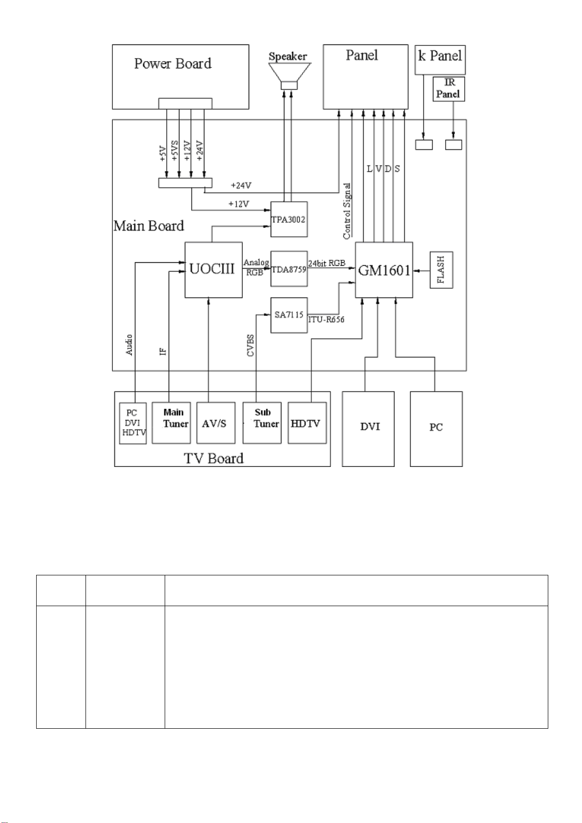
Signal Flow Analysis ................................................................................................................... 22
Manostat Pin Voltage in Main Board Schedule .......................................................................... 25
Main Components and Socket Locations and Definitions ...................................................................25
Main Components Description .................................................................................................... 27
Main Points Wave Illustrations .................................................................................................... 27
CHAPTER FOUR SYMPTOMS AND CORRECTION................................................................................... 33
CHAPTER FIVE LISTS OF BREAKABLE AND MAINTENANCE PARTS ................................34
CHAPTER SIX FACTORY SETUP AND NOTICE....................................................................36
APPENDIX (Schematic Diagram)...................................................................................................................40
1. Schematic Circuit Diagrams
2. Final Assembly Diagram (Take CHD-W320F8 for Example)
3. Final Wiring Connection Diagram (Take CHD-W320F8 for Example)
Designs and specifications are subject to change without notice

3
CHAPTER ONE FEATURES AND COMPOSITIONS
Models for LS08 Chassis:
CHD-W260F8、CHD-W260F8P、CHD-TD260F8
CHD-W270F8、CHD-W270F8P、CHD-TD270F8
CHD-W320F8、CHD-W320F8P、CHD-TD320F8
CHD-W370F8、CHD-W370F8P、CHD-TD370F8
Main Features:
●Radio Frequency input; support CATV
Capable of receiving the full-append cable programs in 470MHZ
●Two-way AV input
Capable of receiving PAL, NTSC, SECAM color systems; Very convenient to watch VCR (video
cassette recorder), Pickup Camera, other Disc’s programs
●AV output
Capable of transmitting signal of different AV/RF systems to other AV receivers through the current
AV cable
●Y/C component signal input (same to S-Video input)
Convenient to receive the Y/C high definition component signal from DVD
●HDTV input
Capable of receiving the high definition YPbPr signal in 480i, 480p, 576i, 720p, 1080i, and 1080p
formats
●VGA input
a. Convenient to connect with the host computer
b. Use as the display terminal
c. Connect the 3.5mm(diameter) audio cord to your computer’s audio main board, you can listening
the beautiful music transmitted from your host computer
●DVI input
Convenient to receive DVI signal
●PIP, POP, PBP function
●Turn on with intelligence
●Zoom mode
●LTI, CTI, and black field
●BBE sound technology
●Trusurround sound technology
●Full-light display
●Picture amending display function
●Super definition display panel
●3:2, 2:2 Pull Down
●TV program scan function
●Timer function
Automatically off at certain preset time, and enters into the standby mode
●Blue background noise reduction
In TV, AV (S-Video), YCbCr, and YPbPr modes, screen displays soft blue background if there is no
signal input
●Auto Off if no signal input
In TV mode, the LCD TV will automatically power off within 15 minutes and enter into the Power

4
Energy Saving Mode if there is no signal input.
●Multi Language On-Screen Display menu
Ordinary and graphical user interface makes the menu operation more user-friendly
●Power Energy Saving Mode (power management mode)
In PC mode, the LCD TV will automatically power off within 30 seconds and enter into the Power
Energy Saving Mode if there is no VGA signal input. It will automatically exit from the Power Energy
Saving Mode and work again when it received a valid VGA signal or press any button on the
panel/remote control.
●Plug and Play
It is no need to equip any installation software when the product is used as computer terminal display
equipment
●Legerity, convenience, low power consumption
●Digital Photo Album Function(Only for CHD-W260F8P/CHD-W270F8P/ CHD-W320F8P/
CHD-W370F8P)
●Built-in DVD Module(Only for CHD-TD260F8 /CHD-TD270F8/CHD-TD320F8/CHD-TD370F8)
⑴Entirely Compatible to DVD、SVCD、VCD、CD、MP3
⑵Compatible to PAL/NTSC Discs
⑶High quality digital audio coaxial input enable you to feel as if sit in the theatre with the perfect classical
hi-fidelity experience
⑷Automatically delete unsuitable parts according to the chosen play levels (max.8 )(only for DVD discs
with play level control)
⑸As many as 32 subtitles
⑹As many as 8 audios
Unit IC Compositions:
LS08 chassis LCD TV is mainly composed of regulator IC、RF IC、video processor IC、Power Amplify
IC、Analog Video IC、System Control IC and Key Control IC, see this IC frame as below:

5
PCB Assembly:
It is mainly composed of TV Board、Remote Control Receiver(Signal Receiver) 、Side AV Board、
K Board and Main Board. Hereunder function introduction to every PCB Assembly:
Numbe
r Parts Description
1 Main Board
Assembly
It is the core of signal processing for LCD TV, which takes responsibility of
transforming outer signal into the uniform digital signal identified by LCD display
with use of System Control IC. TV and AV signals input from TV Board are
decoded by UOCIII to transport RGB signal which is to be transformed by
TDA8759 modulus to transport 24bit RGB digital signal, then it is to be
transformed by GM1601/GM1501 to produce LVDS signal displayed on the
screen, in addition, signals input from VGA、DVI would directly enter into
GM1501 procedure 、format transformation and on screen display.

6
2 TV Board
Assembly
It is mainly composed of two tuners (main and sub tuners) 、AV/S 、HD signal
terminals and some peripheral processing IC. The main tuner demodulates RF
signal to IF signal, and the sub tuner produces CVBS signal, all signals are sent to
the main board after transfer.
3 Remote
Control
Receiver
Assembly
t
is composed of one indicator light and one remote control receiver, which enable
Users operate the TV conveniently and know its current working status simply with
a remote control..
4 Built-in Power
Board
Assembly
It can transform AC 220V into DC for ICs, including +24V,+12V,+5V and +5VS
power supply in standby mode.
5 K Board
Assembly
It consists of 7 function buttons by which users can operate the TV freely.
6 Screen
Assembly
Screens for LS08 have the built-in adverse transformer which change DC into high
voltage AC signal to lighten the back light; The LCD screen is used to display the
image after the image signal has been processed by the main board.
,
7 Side AV Board It is used for earphone output, AV input, S input

7
CHAPTER TWO MAIN ICs FUNCTION INTRODUCTION
GENERAL INTRODUCTION:
TV Board
Number Location Type Main Function
1 UT1 TMI4-C22P2RW Audio and image intermediate frequency signal
output
2 UT2 TAD5-C2IP1RW Sub picture CVBS signal output
Main Board
3 U302,U303 24LC21A T/SN EEPROM
4 U701 24LC32A T/SN Buffer
5 U306,U307,UA3 FSAV330QSCX Switch selection
6 K201 K7262N Audio surface filter
7 K202 K9352N Audio surface filter
8 U6 TPA3002D2PHPR Audio amplifier
9 U801 AM29LV800DT-70EC
Flash,control program inside
10 U700 GM1501-BD Video processor
11 U201 TDA15063H-N1B06557 AV decoder
12 U402 SAA7115HL/V1 Sub channel video decoder
13 U305 SM5302AS-G-ET High definition signal filter
14 U400 TDA8759HV/8/C1 Video signal modulus transformer
15 U5 TDA9178T/N1 Video signal picture amendment
16 U600 MT46V2M32LG-4 Frame buffer
.ICs FUNCTION INTRODUCTION IN DETAILS
Main Tuner (TMI4-C22P2RW)
Pin Definition Description
1 AGC Auto gain control
2 UT NC
3 ADD Ground
4 SCL IIC bus (Clock)
5 SDA IIC bus (Data)
6 NC NC
7 +5V Power supply
8 NC NC
9 30V To produce 0~30V tune voltage
10 NC NC
11 IF Intermediate frequency TV signal
Intermediate frequency TV signal
Sub Tuner (TAD5-C2IP1RW):
Pin Definition Description
1 AGC Auto gain control
2 NC NC

8
3 ADD Ground
4 SCL IIC bus (Clock)
5 SDA IIC bus (Data)
6 NC NC
7 +5V Power supply
8 NC NC
9 33V To produce 0~30V tune voltage
10 NC NC
11 IF Intermediate frequency output (NC)
12 IF Intermediate frequency output (NC)
13 SW0 Band control
14 SW1 Band control
15 NC NC
16 SIF NC
17 AGC Auto gain control
18 VEDIO CVBS signal output
19 +5V Power supply
20 AUDIO NC
GM1501
GM1501is a kind of processing chassis for dual channels image and video, which is mainly used for
LCD displays and integrative TV products. With the resolution of WUXGA, it not only supports PIP
technique, but possesses some IC functions applied to image catch 、process and clock display. It
integrates high velocity AD converter, PLL, high reliability DVI receiver, X86 series miccontrol and LCDS
inverter. See the features as below:
Main Features
●High quality image zoom function;
●Analog RGB signal input interface;
●Intelligent output signal auto identification;
●Integrated high-power PLL output;
●High-reliable self-adaptive DVI input interface;
●4:4:4/4:2:2/CCR656/601 8/16/24bit digital video interface;
●Embedded IC for adjustments of gain、contrast、brightness、color saturation、hue and fleshtone;
●Efficiency in reducing EMI electromagnetism inference;
●Inclined grain processing with small angle;
●High quality video processing;
●Programmable output format;
●Embedded LVDS transport;
●Advanced OSD;
●Embedded micro controller
Pin Description :
Pin Name Description
Analog Signal Input Port

9
L3 AVSYNC ADC vertical synchronization signal input
L4 AHSYNC ADC horizontal synchronization signal input
N2 VGA-SCL VGA lock input
N1 VGA-SDA VGA digital input
D1、D2 RED+、RED- Red analog signal input
C3 SOG Green synchronization signal
C1、C2 GREEN+、- Green analog signal input
B1、B2 BLUE+、BLUE- Blue analog signal input
A2,B3,E3,D3 ADC3.3 ADC3.3Vpower supply
A3,A4 ADC1.8 ADC1.8Vpower supply
A5,B4 ADC-DGND ADC digital ground
C4,D4,E1,E2,E4 ADC-AGND ADC analog ground
DVI Input Output Port
N4 DVI-SCL DDC interface , serial clock signal
N3 DVI-SDA DDC interface ,serial data signal
A6,B6 RXC+,RXC- DVI clock input signal
A8~A10
B8~B10
RX0+~RX2+
RX0-~RX2-
DVI input port
B11 REXT Exterior exit resistance
C6~C11 DVI-3.3 DVI 3.3V power supply
D6、D8~D10 DVI-1.8 DVI 1.8V power supply
A7,A11,B5,B7,C7,D7
D11
DVI-GND DVI ground
Low Bandwidth ADC Port
C13 LBADC-33 ADC3.3Vpower supply
A12,B12,C12 LBADC_IN1~
LBADC_IN3
ADC analog input channel
D12 LBADC_RETURN Channel analog ground
D13 LBADC-GND Power supply voltage analog ground
OCM IC Port
AA1~AA3,Y1~Y3,
W1~W3,V1~V4,
U1~U4,T1~T3
OCMADDR0~
OCMADDR19
Address input output port
AB1~AB3,AC1~AC3,
AD1~AD4,AE1~AE3,
AF1~AF3
OCMDATA0~
OCMDATA15
Data input output port
OCM Port Control Signal
R1,T4,P1,P2 ROM_CSn~
ROM_CS2n
Part selection signal
R2 OCM_REn Read enable signal
R3 OCM_WEn Write enable signal
L1
L2
OCM_INT2
OCM_INT1
Interrupt
M1 OCM_UDO OCM data output
M2 OCM_UDI OCM data input
D25 OCM_TIMER1 OCM timer input

10
Standard Definition Video Control Port
D16 SVCLK SV pels clock input
C14 SVHSYNC SV horizontal synchronization signal input
B14 SVVSYNC SV vertical synchronization signal input
A14 SVODD Scan status input
A17 SVDV SV data input
Standard Definition Video Data Port
D14,D15,A15,A16,
B15,B16,C15,C16
SVDATA7~
SVDATA0
SV ITU656 data input
Video Control Port
A20 VCLK Video pels clock signal
D19 VHS_CSYNC Video horizontal synchronization signal input
C20 VVS Video vertical synchronization signal input
B20 VODD Scan status input
D20 VDV (VSOG) Video data input
B17 VCLAMP Video clamp enable output
A21,A22,A23,B21,
B22,C21,C22,D21
VGRN7~ VGRN0 Green signal or Y signal input
C17,C18,C19,A18
A19,B18,B19,D18
VRED7~ VRED0
Red signal or V/Cr/Pr signal input
B23,B24,B25,A24
A25,C23,C24,D24
VBLU7~ VBLU0
Blue signal or U/Cb/Pb signal input
Screen Control Port
A26 PPWR Screen power control
B26 PBIAS Screen bias control
D26,C25,C26 PWM2 ~PWM0 Pulse width modulation output
AC7 DCLK Pels clock output
AC16 OEXTR Connect external LVDS bias resistance
LVDS Port
AE14~AE16,AE19~
AE23,AF13~AF16
AF19~AF23,AF11
A0-~A3-, A0+~A3+
B0-~B3-, B0+~B3+
Low voltage difference data input
AD14,AD11,AE13
AE11,AC11,AF10
LVDS_SHIELD[5] ~
LVDS_SHIELD[0]
Low voltage difference protect output
AE12,AF12,
AF20,AE20
AC+,AC-,BC+,BC- Low voltage difference protect input
Screen Port Power Supply
AD12,AD13,AC12 LVDSB_3.3 LVDS B channel power supply
AC13,AC14,AC15 LVDSB_GND B channel ground
AC20,AC21,AC22 LVDSA_3.3 LVDS A channel power supply
AD19,AC19,AC20 LVDSA_GND A channel ground
AE17 VDDD33_LVDS Analog power supply
AD17 VSSD33_LVDS Analog ground
Clock Composite and Power Supply
G4 XTAL crystal oscillator interface

11
F2 VDDD33_PLL,
H1 VDDD33_SDDS
J1 VDDD33_DDDS
Digital power supply
G2 VSSD33_PLL
J4 VSSD33_SDDS
K4 VSSD33_DDDS
Digital ground
F4 VDDA33_RPLL
G1 VDDA33_FPLL
H3 VDDA33_SDDS
J3 VDDA33_DDDS
Analog power supply
F3 VSSA33_RPLL
H4 VSSA33_FPLL
H2 VSSA33_DDDS
J2 VSSA33_DDDS
Analog ground
G3 TCLK Reference clock signal input
K2 ACS_RSET_HD External resistance port
System Signal
K1 RESETn Reset signal
M3,M4 IR0,IR1
P4 MSTR_SCL Main clock output signal
P3 MSTR_SDA
Main data output/input signal 信号
R4 EXTCLK External clock input
Frame Storage Interface
U24,U23 FSCLKp,FSCLKn Fine storage clock output
V24,V25 FSRAS,FSCAS Address output
V26 FSWE Write enable port
W26 FSCKE Read enable port
J24 FSVREF Reference voltage input
K26 FSVREFVSS Reference voltage ground
W25 FSVREF Reference voltage input
W24 FSVREFVSS Reference voltage ground
L26 FSDQS Data filter
F24~F26,G23~G26
H24~H26,J25,J26,
R24~R26,P24~P26
N23~N26,…….
FSDATA31~
FSDATA0
Data input output port
T24,T25,U25,U26 FSDQM3~ FSDQM0 Data output mark
Y26
Y25
FSBKSEL1,
FSBKSEL0
Layer address
AA24~AA26
AB24~AB26,
AC24~AC26
AD24~AD26
FSADDR11~
FSADDR0
Range address output
E23, F23, H23, J23,
L23,M23,P23, R23,
T23,V23,W23,Y23,
FS_2.5
2.5V power supply

12
AA23,AB23,AC23
K23 VDDA18_DLL 1.8V power supply
K25 VSSA18_DLL Power supply ground
Digit power supply
K10,K11,K16,K17,
L11,L16,T11,T16,
T17,U10,U11,U16,U17
CORE_1.8 1.8V power supply
D23, W4,Y4, AA4,
AB4,AC4,AC6,D17,
D22,AC8,AC10
IO_3.3
3.3V power supply
K12,K13,K14,K15,
L10,L12,L13,L14,
L15,L17,M10,M11,
M12,M13。。。。。。
D_GND
Power ground
A1,AC,D5,AC17,
K3,F1
NO_CONNECT
NC
GM1501Internal Diagram:
TDA8759:
TDA8759 is a triple 8-bit video converter interface. The IC converts a RGB analog signal into a 24bit
RGB or YUV or YCbCr digital signal , or converts a YUV or YCbCr analog signal into a YUV or RGB digital
signal with a sampling rate up to 81 Msps. The IC supports resolutions from 480i and VGA to HDTV and
XGA.

13
Main Features:
●Triple 8-bit Analog-to-Digital Converter (ADC)
●Three independent analog video sources up to 81 Msps selectable by I2C-bus
●Auto check on interval scan video signal
●1.8Vand 3.3Vsupplies
●Low gain variation with temperature
●Output format RGB 4:4:4, YUV 4:4:4, YUV 4:2:2 ,CCIR 656 or YUV 4:2:2 semi-planar standard on
output bus;
●I²C bus control
●Programmable clock phase adjustment cells
●Amplifier bandwidth of 100 MHz
●Integrated PLL divider
●Power-Downmode
TDA8759 Internal Diagram:
Pin Description:
Pin Name Description
1 HREF Horizontal reference output
2 VCLK Video clock output
3,13,21,29,
37,45,164
VDDO Video port output supply voltage

14
4,14,22,30
38,46,165
OGND Video port output
ground
7,8,9,10,
15,16,17,18
VPA0~VPA7 Video port A
11,116,130,132 VDDC Power supply port
12,117,159 CGND Ground
23~28,31,32 VPB0~VPB7 Video port B
35,36,39~44 VPC0~VPC7 Video port C
47,53,57,58,55
60,66,70,71,75
81,83,85,86,
AGND Analog ground
48,54,59,61,67
69,76,82,85,87,88
VDDA Power supply port
49 REFB/Pb Blue/blue-chrominance channel reference input
52,51,50 B/Pb1~ B/Pb3 Blue/blue-chrominance channel analog input
56 BIAS Bias input
62 REFG/Y Green/green-chrominance channel reference
input
65,64,63 G/Y1~G/Y3 Green/green-chrominance channel analog input
74,73,72 SOG/Y1~SOG/Y3 Sync on green//brightness channel input
77 REFR/Pr Red/red-chrominance channel reference input
80,79,78 R/Pr1~ R/Pr3 Red/red-chrominance channel analog input
89~92,97~101
112,121,122,
124,125,160~163
TST0~TST17 Reserved for test
93 PD Power-down control input
94 OE Output enable input
96 A0 I²C bus address control input
102 COAST PLL control input
103 GAIN Gain input
104 CLAMP Clamp input
105~107 VSYNC1~VSYNC3 Vertical synchronization input
108~110 H(C)SYNC1~
H(C)SYNC3
Horizontal (composite)synchronization input
111 CKEXT External clock input
113 TCLK Reserved for test
114 DIS I²C bus disable control input
118 SDA I²C bus data input/output
119 SCL I²C bus clock input
120,126,127,131
133,142,148,
IGND Input digital ground
123,138,139,145
151,157
VDDI Input digital supply voltage
166 PL PLL disable belock output
167 DE Data enable output

15
168 HS Horizontal synchronization input
169 VS vertical synchronization input
170 CS Color synchronization output
171 ORR/V Red / chrominance ADC output
172 ORB/U Blue /chrominance ADC output
173 ORG/Y Green / chrominance ADC output
174 VAI Video dynamic indication output
175 FREF Scan output
17 VREF Vertical channel reference input
TPA3002D2:
The TPA3002D2 is a 9-W (per channel) efficient, Class-D audio amplifier for driving bridged-tied stereo
speakers. The TPA3002D2 can drive stereo speakers as low as 8 . The high efficiency of the TPA3002D2
eliminates the need for external heatsinks when playing music.
Main Features:
●9W /Ch into an 8Ωload from 12Vsupply;
●Efficient, class D operation eliminates heatsinks and reduces power supply requirements;
●32-step DC volume control from -40db~36db;
●Line outputs for external headphone;
●Thermal and short-circuit protection
Pins Functions:
Pin Name Description
26, 30 AGND Analog ground for digital/analog cells in core
33 AVCC High-voltage analog power supply(8~14V)
29 AVDD 5V regulated output capable of 100mA output
7 AVDDREF Reference 5V output
13 BSLN
24 BSLP
Bootstrap I/O left channel
48 BSRN
37 BSRP
Bootstrap I/O right channel
28 COSC I/O for charge/discharge currents onto capacitor for ramp generator
triangle wave
6 LINN
5 LINP
Negative differential audio input for left channel
Positive differential audio input for left channel
16,17 LOUTN
20,21 LOUTP
Class-D 1/2-H-bridge negative output for left channel
Class-D 1/2-H-bridge positive output for left channel
34 MODE Input for MODE control. A logic high on this pin places the amplifier in
the variable output mode and the Class-D outputs are disabled. A logic
low on this pin places the amplifier in the Class-D mode and Class-D
stereo outputs are enabled. Variable outputs (VAROUTL and
VAROUTR) are still enabled in Class-D mode to be used as line-level
outputs for external amplifiers.
35 MODE_OUT Output for control of the variable output amplifiers. When the MODE pin

16
(34) is a logic high, the MODE_OUT
pin is driven low. When the MODE pin (34) is a logic low, the
MODE_OUT pin is driven high. This pin is
intended for MUTE control of an external headphone amplifier. Leave
unconnected when not used for
headphone amplifier control.
18,19,42,4
3
PGNDR,PGNDL Power ground for left channel H-bridge Power ground for right
channel H-bridge
14,15,22,2
3
PVCCL
38,39,46,4
7
PVCCR
Power supply for left channel H-bridge (tied to pins 22 and 23
internally), not connected to PVCCR or AVCC.
PVCCL 22, 23 – Power supply for left channel H-bridge (tied to pins 14
and 15 internally), not connected to PVCCR or AVCC.
PVCCR 38,39 – Power supply for right channel H-bridge (tied to pins 46
and 47 internally), not connected to PVCCL or AVCC.
PVCCR 46, 47 – Power supply for right channel H-bridge (tied to pins
38 and 39 internally), not connected to PVCCL or AVCC.
12 REFGND Ground for gain control circuitry. Connect to AGND. If using a DAC to
control the volume, connect the DAC ground to this terminal.
32 RINP
2 RINN
Positive differential audio input for right channel
Negative differential audio input for right channel
27 ROSC Current setting resistor for ramp generator. Nominally equal to 1/8*
44,45,
40,41
ROUTN, ROUTP Class-D 1/2-H-bridge negative output for right channel
ROUTP 40, 41 O Class-D 1/2-H-bridge positive output for right channel
1 SD Shutdown signal for IC (low = shutdown, high = operational). TTL logic
levels with compliance to VCC.
9 VARDIFF DC voltage to set the difference in gain between the Class-D and
VAROUT outputs. Connect to GND or AVDDREF if VAROUT outputs
are unconnected.
10 VARMAX DC voltage that sets the maximum gain for the VAROUT outputs.
Connect to GND or AVDDREF if VAROUT outputs are unconnected.
31 VAROUTL Variable output for left channel audio. Line level output for driving
external HP amplifier.
32 VAROUTR VAROUTR 32 O Variable output for right channel audio. Line level
output for driving external HP amplifier.
25 VCLAMPL VCLAMPL 25 – Internally generated voltage supply for left channel
bootstrap capacitors.
36 VCLAMPR Internally generated voltage supply for right channel bootstrap
capacitors.
11 VOLUME DC voltage that sets the gain of the Class-D and VAROUT outputs.
8 VREF Analog reference for gain control section.
4 V2P5 2.5-V Reference for analog cells, as well as reference for unused audio
input when using single-ended inputs.
TPA3002D2 Internal Diagram:

17
SM5301AS :
order Butterworth lowpass filter configuration. The filter characteristics have been optimized for
minimal overshoot and flat group delay, it has a variable cutoff frequency and guaranteed driver-stage
channel gain difference and phase difference values.
Main Features:
●supply voltage:5V±10%;
●_DC voltage level restore sync clamp function
●Output buffer gain switching function: 0, 6dB (input-to-output AC signal gain)
●Channel-to-channel gain difference: 0.5dB(±5% supply voltage variation);
●Channel-to-channel phase difference: 3.5 degree
●Output signal harmonic distortion (all channels):1.5%
●Cutoff frequency: 5.8 to 37MHz variable
SM5301AS Internal Diagram:

18
Pin Description:
Pin Name Description
2 GSG1 GOUT/UOUT output buffer gain set input
1 GINA/UINA
3 GINB/UINB
Analog GINA or UINA signal input. Sync signal is input on SYNCIN
pin.
Analog GINB or UINB signal input. Sync signal is input on SYNCIN
pin.
5 BINA/VINA
7 BINB/VINB
Analog BINA or VINA signal input. Sync signal is input on SYNCIN
pin.
Analog BINB or VINB signal input. Sync signal is input on SYNCIN
pin
6 GSB1 BOUT/VOUT output buffer gain set input
9 DISABLE Power save function. Built-in pull-down resistor.
10,13,16,19 GND Ground
11 BOUT/VOUT B/V signal output
14 GOUT/UOUT Analog 5V supply
17 ROUT/YINB R/Y signal output
12,15,18,24 VCC Analog 5V supply
20 RFC LPF (lowpass filter) cutoff frequency setting resistor connection
21 VFC LPF (lowpass filter) cutoff frequency setting voltage input
22 MUXSEL Input select signal
23 SYNCIN Filter channel external H-Sync signal input.
26 GSR1 ROUT/YOUT output buffer gain set input
25 RINA/YINA
27 RINB/YINB
Analog RINA or YINA signal input. Sync signal is input on SYNCIN
pin.
Analog RINB or YINB signal input. Sync signal is input on SYNCIN
pin.

19
4,8,28 NC No connection(leave open or connect to ground)
SAA7115:
The SAA7115 is a video capture device for various applications ranging from small screen products like
e.g. digital set top boxes, personal video recording applications to big screen devices like e.g. LCD
projectors due to it’s improved comb filter performance and 10 bit video output capabilities.
Main Features:
●Six analog inputs, internal analog source selectors;
●Two improved 9 Bit CMOS analog-to-digital converter in differential CMOS style;
●Automatic Clamp Control (ACC) for CVBS, Y and C;
●Enhanced Horizontal and vertical Sync Detection;
●PAL delay line for correcting PAL phase errors;
●Automatic TV/VCR detection;
SAA7115 Internal Diagram:
Pin Function:
Pin Name Description
1,8,11,17,23,25,33
43,51,58,68,75,83
93
VDD Supply voltage port
2 TDO Test Data Output for Boundary Scan Test (2)
3 TDI Test Data Input for Boundary Scan Test (with internal pull-up)(2)
4 XTOUT crystal oscillator output signal, auxiliary signal
6 XTALO 24.576 (32.11) MHz crystal oscillator output; not connected if XTALI is

20
7 XTALI driven
by an external single-ended oscillator.
Input terminal for 24.576 (32.11) MHz crystal oscillator or connection
of external oscillator with TTL compatible square wave clock signal.
6 VXDD Crystal oscillator power supply
10,12,14,16 AI21~AI24 Analog signal input 21~24
13 AI2D
19 AI1D
differential input for ADC channel 2 (pins AI24, AI23, AI22, AI21)
differential input for ADC channel 1 (pins AI12, AI11)
20 AI11
18 AI12
analog input 11
analog input 12
5,9,15,21,24,26,38
50,63,76,88,100
AGND
VSS
ground
22 AOUT Analog test output (do not connect)
27 CE Chip Enable or RESET input (with internal pull up)
28 LLC
29 LLC2
line-locked system clock output (27 MHz nominal), for backward
compatibility,
do not use for new applications
line locked clock/2 output (13.5 MHz nominal) for backward
compatibility, do
not use for new applications
30 RESON RESet Output Not signal
31 SCL IIC serial clock line (with inactive output path)
32 SDA IIC serial data line
34 RTS0
35 RTS1
real time status or sync information, controlled by subaddr. “11h and
12h”
RTS1 35 O real time status or sync information, controlled by
subaddr. “11h and 12h”
36 RTCO Real time control output
37 AMCLK Audio master clock output
39 ASCLK Audio serial clock output
40 ALRCLK Audio lift/right clock output
41 AMXCLK Audio master external clock input
42 ITRDY Target ready input, image port(with internal pull up)
45 ICLK clock output signal for image-port, LCLK of LPB image port mode, or
optional
asynchron. backend clock input
46 IDQ output data qualifier for image port (optional: gated clock output)
47 ITRI image-port output control signal, effects all I-port pins incl. ICLK,
enable and active polarity is under software control (bits IPE in
subaddr. “87”) output path used for Testing: scan output
48 IGP0
This manual suits for next models
1
Table of contents
Other Akai TV manuals

Akai
Akai 25CT23FSR User manual

Akai
Akai PDP4273M User manual

Akai
Akai P42L6A-T1 User manual

Akai
Akai LCT2765TD User manual

Akai
Akai 21CTS92FS User manual

Akai
Akai LTA-26C902 User manual

Akai
Akai LT-2605AB User manual

Akai
Akai DLC-E2452S/4G User manual

Akai
Akai PT50DL24 User manual

Akai
Akai LCT2016 User manual

Akai
Akai ATE-24014 CNK User manual

Akai
Akai ALED3205TBK User manual

Akai
Akai CT-1420ANF User manual

Akai
Akai PDP4210EA1 User manual

Akai
Akai CT-T29S32S User manual

Akai
Akai LCT-4216 User manual

Akai
Akai NXT2766 User manual

Akai
Akai CT-S21MTD-E3 User manual

Akai
Akai PT50DL14 User manual

Akai
Akai 29CT24FS User manual