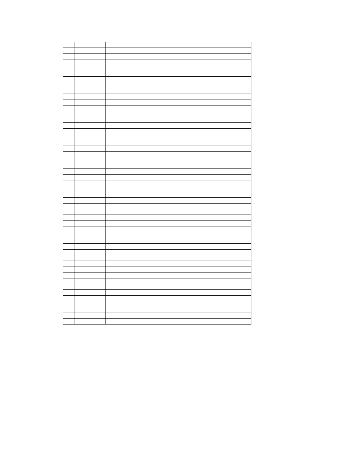
Alcor AU9321 Product manual

AU9321
USB Compact Flash Card Reader
Technical Reference Manual
Revision 1.1
© 1997-2002 Alcor Micro Corp.
All Rights Reserved

Copyright Notice
Copyright 1997 - 2002
Alcor Micro Corp.
All Rights Reserved.
Trademark Acknowledgements
The company and product names mentioned in this document may be the trademarks or registered trademarks of their manufacturers.
Disclaimer
Alcor Micro Corp. reserves the right to change this product without prior notice.
Alcor Micro Corp. makes no warranty for the use of its products and bears no responsibility for any error that appear in this document.
Specifications are subject to change without prior notice.
Contact Information:
Web site: http://www.alcormicro.com/
Taiwan
Alcor Micro Corp.
4F-1, No 200 Kang Chien Rd., Nei Hu,
Taipei, Taiwan, R.O.C.
Phone: 886-2-8751-1984
Fax: 886-2-2659-7723
Santa Clara Office Los Angeles Office
2901 Tasman Drive, Suite 206 9400 Seventh St., Bldg. A2
Santa Clara, CA 95054 Rancho Cucamonga, CA 91730
USA USA
Phone: (408) 845-9300 Phone: (909) 483-9900
Fax: (408) 845-9086 Fax: (909) 944-0464

TABLE OF CONTENTS i
Table of Contents
1.0 Introduction-------------------------------------------------------------------------------------- 1
1.1 Description---------------------------------------------------------------------------------- 1
1.2 Features-------------------------------------------------------------------------------------- 1
2.0 Application Block Diagram----------------------------------------------------------------- 3
3.0 Pin Assignment-------------------------------------------------------------------------------- 5
4.0 System Architecture and Reference Design----------------------------------------- 7
4.1 AU9320 Block Diagram------------------------------------------------------------------ 7
4.2 Sample Schematics------------------------------------------------------------------------ 8
5.0 Electrical Characteristics------------------------------------------------------------------- 9
5.1 Recommended Operating Conditions------------------------------------------------- 9
5.2 General DC Characteristics ------------------------------------------------------------ 9
5.3 DC Electrical Characteristic for 3.3--------------------------------------------------- 9
5.4 Crystal Oscillator Circuit Setup for Characteristics ------------------------------ 10
5.5 ESD Test Results -------------------------------------------------------------------------- 11
5.6 Latch-Up Test Results ------------------------------------------------------------------- 12
6.0 Mechanical Information---------------------------------------------------------------------- 15

TABLE OF CONTENTS i

INTRODUCTION 1
1.0 Introduction
1.1 Description
The AU9321 is a single chip integrated USB Compact Flash (CF) card reader controller. It
can be used as a removable storage disk in enormous data exchange applications between PC
and PC or PC and various consumer electronic devices.
The AU9321 can read of CF card’s contents created by handheld consumer electronic devices
such as digital camera, MP3 player, PDA and mobile phone… etc. It provides a faster and
convenient way of data transfer scheme to meet the emerging need of a data exchange center
between PC and various consumer devices. With AU9320, users’ experience will be further
enhanced by the Plug-and-Play nature built into latest operation systems such as Windows
2000/XP and Mac OS X.
Because of the multiple sectors transfer up to 4G bytes and the single chip integration,
AU9321 will be the most powerful and cost efficient CF card reader controller solution in the
market.
1.2 Features
Fully compliant with USB v1.1 specification and USB Device Class Definition for
Mass Storage, Bulk-Transport v1.0
Fully compliant with Compact Flash (CF) v1.4 Specification.
Work with default driver from Windows ME, Windows 2000, Windows XP, Mac
OS 9.1, and Mac OS X. Windows 98 is supported by vendor driver from Alcor.
Ping-pong FIFO implementation for concurrent bus operation
Support multiple sectors transfer up to 4G byte to optimize performance
Support optional external EEPROM for USB VID, PID and string customization
Capable of handling 8 sets of built-in PID, VID and strings to minimize inventory
control and improve lead production lead time
LED for bus activity monitoring
Integrated power switch and power management circuit to meet USB 500uA power
consumption during suspend with CF card in the slot.
Runs at 12MHz, built-in 48 MHz PLL
Built-in 3.3V regulator
48-pin LQFP package

INTRODUCTION 2

APPLICATION BLOCK DIAGRAM 3
2.0 Application Block Diagram
Following is the application diagram of a typical flash memory card reader using AU9321. By
connecting the reader to a PC through USB bus, the AU9321 is acting as a bridge between the
flash memory card from digital camera, MP3 player, PDA or mobile phone and PC.
PCwithUSBHost Controller
USB Flash
Card Reader
Moble Phones
PDA
MP3 Player
Digital Camera
CF Cards
PC

APPLICATION BLOCK DIAGRAM 4

PIN ASSIGNMENT 5
3.0 Pin Assignment
The AU9321 is packed in 48-LQFP form factor. The following figure shows signal name for
each pin and the table in the following page describes each pin in detail.
1
2
3
5
4
6
7
8
10
9
11
33
32
31
29
30
34
46 45 44 43 42
12
35
36
28
27
26
25
41 40 39 38 374748
13 14 15 16 17 18 19 20 21 22 23 24
XTAL 1
XTAL 2
VCCA
GNDA
VCC2CF
VCC5V
VCC3V
USB_DM
USB_DP
RSTN
GNDIO
PDPD
EEP
DATA
EEP
CLK
CF
WEN
GND
CFD3
PDCFPD GND
GND
GND
GND
CFRST
CFWTN
CFOEN
CFAD9
VCCK
GNDK
CFAD3
CFAD2
CT2
IOWRN
IORDN
CFCDN
CFAD0
CFAD1
GPI0
GPI1
GPI2
GPO6
CTI
GPO7
CFD4
CFD7
CFD6
CFD5
CFD1
CFD0
CFD2

PIN ASSIGNMENT 6
Table 3-1. Pin Descriptions
Pin Name IO Type Description
1 XTAL1 Input Crystal Oscillator Input (12MHz)
2 XTAL2 Output Crystal Oscillator Output (12MHz)
3 VCCA Power Analog Vcc, Connected to 3.3V
4 GNDA Ground Connected to Ground
5 VCC2CF Power CF Power
6 VCC5V Power 5V Power Supply
7 VCC3V Output Regulated 3.3V out
8 USB_DM Input/Output USB D-
9 USB_DP Input/Output USB D+
10 RSTN Input Hardware reset (Active Low)
11 GNDIO Ground Ground
12 CFPD Power Power Down
13 EEPDATA Input/Output EEPROM Data
14 EEPCLK Output EEPROM Clock
15 CFWEN Output Arribute write enable
16 GND Ground Ground
17 CFD3 Input/Output Compact Flash Data 3
18 CFD4 Input/Output Compact Flash Data 4
19 CFD5 Input/Output Compact Flash Data 5
20 CFD6 Input/Output Compact Flash Data 6
21 CFD7 Input/Output Compact Flash Data 7
22 CFD0 Input/Output Compact Flash data 0
23 CFD1 Input/Output Compact Flash data 1
24 CFD2 Input/Output Compact Flash data 2
25 GND Ground Ground
26 GND Ground Ground
27 GND Ground Ground
28 GND Ground Ground
29 CFRST Output Compact Flash reset signal
30 CFWTN Input Compact Flash wait signal
31 CFOEN Output Compact Flash output enable
32 CFAD9 Output Compact Flash address 9
33 CFAD3 Output Compact Flash address 3
34 CFAD2 Output Compact Flash address 2
35 VCCK Power Kernel Vcc
36 GNDK Ground Kernel Ground
37 CT2 Connected to Ground
38 IOWRN Output Compact Flash I/O write signal
39 IORDN Output Compact Flash I/O read signal
40 CFCDN Input Compact Flash Card Detect
41 CFAD0 Output Compact Flash address 0
42 CFAD1 Output Compact Flash address 1
43 GPI0 Input General Purpose I (*1)
44 GPI1 Input General Purpose I (*1)
45 GPI2 Input General Purpose I
46 GPO6 Output General Purpose Output
47 GPO7 Output General Purpose Output, used for LED activity
48 CT1 Connected to Ground

SYSTEM ARCHITECTURE AND REFERENCE DESIGN 7
4.0 System Architecture and
Reference Design
4.1 AU9321 Block Diagram
Alcor Micro - AU9321 Flash Memory Card Reader Block Diagram
USB
SIE
USB
Upstream
Port
XCVR
RAM
3.3 V
Voltage
Regulator
/Power Switch
3.3 V
Processor ROM
12MHz
XTAL
POR
CF control
FIFO
Card
Power
EEPROM
CF
EEPROM
Control
Reset

SYSTEM ARCHITECTURE AND REFERENCE DESIGN 8
4.2 Sample Schematics
CFD7
CFD7
TP
CARD POWER
CFCDN
CFOEN
CFD2
R12
1M
GNDK
CFRDN
CFWTN
F6
FB
R20 10K
CFRDN
R10 1K
VCC3.3
CFAD9
GPO7
C3
1UF
R13 10K
CFD0
VCC2CF
R4 39
XTAL1
R16 10K
CFD1
VCCA
C11
0.1UF
CFAD1
RSTN
R19 10K
Y1
12MHZ
C12 18PF
R6
10K
CARD POWER
CFAD2
C9 18PF
Disclaimer: This schematic is for reference only.
Alcor Micro Corp. makes no warranty for the use of its
products and bears no responsibility for any error that
appear in this document. Specifications are subject to
change without notice.
CARD POWER
C8
0.1UF
CFAD1
F5
FB
CFWRN
CFD3
R7330
F3
FB
R9
10K
EEPCLK
CT1
R18 10K
VCC3.3
VCCK
CFD5
A4
11Wednesday, July 24, 2002
1.1
AU9321 Demostration schematic
Size Document Number Rev
Date: Sheet of
CFD3
CFWEN
CFD4
CFD2
CFD2
C4
0.1UF
F2FB
C1
0.1UF
R5
100K
VCC
VCC3.3
XTAL1
VCC3.3
CFWRN
R1
1.5K
CFWEN
CFD6
CFD6
CFD5
VCC3.3
CFOEN
C2
10UF
R17 10K
VCC
CFD5
VCC5V
CARD POWER
R11
330
CFCDN
GPO7
VCCA
R15 10K
XTAL2
CFD0
C13
0.1UF
CFAD3
GNDK
C10
0.1UF
D1
VCC3.3
VCC3.3
XTAL2
TP
GNDIO
C6
0.1UF
CFAD3
VCC5V
CFD0
EEPCLK
VCC3.3
U3
AU9321-48PIN
1
2
3
4
5
6
7
8
9
10
11
13
14
15
17
18
19
20
21
22
23
24
48
47
46
45
44
43
42
41
40
39
38
36
35
34
33
32
31
30
29
27
26
25
12
16
28
37
XTAL1
XTAL2
VCCA
GNDA
VCC2CF
VCC5V
VCC3V
USB_DM
USB_DP
RSTN
GNDIO
EEPDATA
EEPCLK
CFWEN
CFD3
CFD4
CFD5
CFD6
CFD7
CFD0
CFD1
CFD2
CT1
GPO7
GPO6
GPI2
GPI1
GPI0
CFAD1
CFAD0
CFCDN
CFRDN
CFWRN
GNDK
VCCK
CFAD2
CFAD3
CFAD9
CFOEN
CFWTN
CFRST
GND
GND
GND
CFPD
GND
GND
CT2
CFAD9
F1
FB
GNDA
VCCK
R8
1M
J1
CF CONNECTOR
1
3
5
7
9
11
13
15
17
19
21
23
25
27
29
31
33
35
37
39
41
43
45
47
49 50
48
46
44
42
40
38
36
34
32
30
28
26
24
22
20
18
16
14
12
10
8
6
4
2
GND
CFdata4
CFdata6
CE1N
-OE
CFaddr8
VCC
CFaddr5
CFaddr3
CFaddr1
CFdata0
CFdata2
CDN
CFdata11
CFdata13
CFdata15
VS1
IOWRN
INTRQ
CSEL
RESET
INDACK
SPKR
CFdata8
CFdata10 GND
CFdata9
STSCHG
REGN
WAITN
VS2
VCC
WEN
IORDN
CE2N
CFdata14
CFdata12
CDN
IOIS16
CFdata1
CFaddr0
CFaddr2
CFaddr4
CFaddr6
CFaddr7
CFaddr9
CFaddr10
CFdata7
CFdata5
CFdata3
R14 10K
TP
CFAD2
CFRST
CFD1
GNDA
CFAD0
R2
100K
ACTIVITY LED
CFD7
EEPDATA
VCC2CF
C5
0.1UF
Q2
1N9013
U2
24C01A or compatible
1
2
3
45
6
7
8A0
A1
A2
GNDSDA
SCL
WP
VCC
GNDIO
F4
FB
R3 39
C7
0.1UF
CFRST
CFWTN
CFAD0
CFD4
CFD1
INTRQ
VCC
CFD6
Q1
HBC807 or compatible
J1 1
2
3
4
5
VCC
DATA-
DATA+
GND
FGND1
CFD3
EEPDATA
CFD4

ELECTRICAL CHARACTERISTICS 9
5.0 Electrical Characteristics
5.0 Recommended Operating Conditions
SYMBOL PARAMETER MIN TYP MAX UNITS
VCC Power Supply 4.75 5 5.25 V
VIN Input Voltage 0 VCC V
TOPR Operating Temperature 0 85 OC
TSTG Storage Temperature -40 125
OC
5.1 General DC Characteristics
SYMBOL PARAMETER CONDITIONS MIN TYP MAX UNITS
IIL Input low current no pull-up or pull-down -1 1 µA
IIH Input high current no pull-up or pull-down -1 1 µA
IOZ Tri-state leakage current -10 10 µA
CIN Input capacitance 5 ρF
COUT Output capacitance 5 ρF
CBID Bi-directional buffer capacitance 5 ρF
5.2 DC Electrical Characteristics for 3.3 volts operation
SYMBOL PARAMETER CONDITIONS MIN TYP MAX UNITS
VIL Input Low Voltage CMOS 0.9 V
VIH Input Hight Voltage CMOS 2.3 V
VOL Output low voltage IOL=4mA, 16mA 0.4 V
VOH Output high voltage IOH=4mA,16mA 2.4 V
RIInput Pull-up/down resistance Vil=0V or Vih=VCC 10k/200k KΩ

ELECTRICAL CHARACTERISTICS 10
5.4 Crystal Oscillator Circuit Setup for Characteristics
The following setup was used to measure the open loop voltage gain for crystal oscillator
circuits. The feedback resistor serves to bias the circuit at its quiescent operating point and
the AC coupling capacitor, Cs, is much larger than C1 and C2.

ELECTRICAL CHARACTERISTICS 11
5.5 ESD Test Results
Test Description : ESD Testing was performed on a Zapmaster system using the Human-
Body –Model (HBM) and Machine-Model (MM), according to MIL_STD 883 and EIAJ
IC_121 respectively.
Human-Body-Model stress devices by sudden application of a high voltage supplied
by a 100 PF capacitor through 1.5 Kohm resistance.
Machine-Model stresses devices by sudden application of a high voltage supplied by a
200 PF capacitor through very low (0 ohm) resistance
Test circuit & condition
Zap Interval : 1 second
Number of Zaps : 3 positive and 3 negative at room temperature
Critera : I-V Curve Tracing
Model Model S/S TARGET Results
HBM Vdd, Vss, I/C 15 4000V Pass
MM Vdd, Vss, I/C 15 200V Pass

ELECTRICAL CHARACTERISTICS 12
5.6 Latch-Up Test Results
Test Description: Latch-Up testing was performed at room ambient using an
IMCS-4600 system which applies a stepped voltage to one pin per device with
all other pins open except Vdd and Vss which were biased to 5 Volts and
ground respectively.
Testing was started at 5.0 V (Positive) or 0 V(Negative), and the DUT was
biased for 0.5 seconds.
If neither the PUT current supply nor the device current supply reached the
predefined limit (DUT=0 mA , Icc=100 mA), then the voltage was increased
by 0.1 Volts and the pin was tested again.
This procedure was recommended by the JEDEC JC-40.2 CMOS Logic
standardization committee.
Notes:
1. DUT: Device Under Test.
2. PUT: Pin Under Test.
Vcc
DUT
GND
Pin
under
m
Untested
Output Open
Circui
t
Untested
Input Tied
to V supply
Trigger
Sou
r
ce
V Su
pp
l
y
+
+
Icc Measurement
1 Source
Test Circuit : Positive Input/ output Overvoltage /Overcurrent

ELECTRICAL CHARACTERISTICS 13
Vcc
DUT
GND
Pin
under
test
mA
Untested
Output Open
Circuit
Untested
Input Tied
to V supply
Trigger
Source
V Supply
+
+
Icc Measurement
Test Circuit : Negative Input/ Output Overvoltage /Overcurrent
1 Source
Vcc
DUT
GND
mA
Untested
Output Open
Circuit
All Input Tied
to V supply
V Supply
+
Icc Measurement
Supply Voltage test
Latch–Up Data
Model Model Voltage (v)/ Current (mA) S/S Results
+Voltage - 11.0
11.0 5 Pass
+Current - 200
200 5
Vdd-Vxx 9.0 5 Pass

ELECTRICAL CHARACTERISTICS 14

MECHANICAL INFORMATION 15
6.0 Mechanical Information
body size lead
D1 E1
count A1 A2 L1 b c e
7 7 48 0.1 1.4 1 0.2 0.127 0.5
A1 stand-off
A2 body thickness
L1 lead length
b lead width
c lead thickness
e lead pitch

All Datasheets Cannot Be Modified Without Permission
Copyright © Each Manufacturing Company
This datasheet has been downloaded from:
www.EEworld.com.cn
Free Download
Daily Updated Database
100% Free Datasheet Search Site
100% Free IC Replacement Search Site
Convenient Electronic Dictionary
Fast Search System
www.EEworld.com.cn
Table of contents
Other Alcor Card Reader manuals
Popular Card Reader manuals by other brands

TAGSYS RFID
TAGSYS RFID Textile L100 user guide

Lindy
Lindy 42768 user manual

Excelsecu Data Technology
Excelsecu Data Technology eSecu FIDO2 user manual

ICP DAS USA
ICP DAS USA ACS-11-MF user manual

Paxton
Paxton PROXIMITY LCD Ins-30091 quick start guide

Star Micronics
Star Micronics TCP300V Series Operation manual