Alcor AU9381 Product manual

AU9381
USB Flash Disk Controller
Technical Reference Manual
Revision 1.2
© 1997-2003 Alcor Micro Corp.
All Rights Reserved

Copyright Notice
Copyright 1997 - 2003
Alcor Micro Corp.
All Rights Reserved.
Trademark Acknowledgements
The company and product names mentioned in this document may be the trademarks or registered trademarks of their manufacturers.
Disclaimer
Alcor Micro Corp. reserves the right to change this product without prior notice.
Alcor Micro Corp. makes no warranty for the use of its products and bears no responsibility for any error that appear in this document.
Specifications are subject to change without prior notice.
Contact Information:
Web site: http://www.alcormicro.com/
Taiwan
Alcor Micro Corp.
4F-1, No 200 Kang Chien Rd., Nei Hu,
Taipei, Taiwan, R.O.C.
Phone: 886-2-8751-1984
Fax: 886-2-2659-7723
Santa Clara Office Los Angeles Office
2901 Tasman Drive, Suite 206 9400 Seventh St., Bldg. A2
Santa Clara, CA 95054 Rancho Cucamonga, CA 91730
USA USA
Phone: (408) 845-9300 Phone: (909) 483-9900
Fax: (408) 845-9086 Fax: (909) 944-0464

TABLE OF CONTENTS i
Table of Contents
1.0 Introduction-------------------------------------------------------------------------------------- 1
1.1 Description---------------------------------------------------------------------------------- 1
1.2 Features-------------------------------------------------------------------------------------- 1
2.0 Application Block Diagram----------------------------------------------------------------- 3
3.0 Pin Assignment-------------------------------------------------------------------------------- 5
4.0 System Architecture and Reference Design----------------------------------------- 9
4.1 AU9381 Block Diagram------------------------------------------------------------------ 9
4.2 Sample Schematics------------------------------------------------------------------------ 10
5.0 Electrical Characteristics------------------------------------------------------------------- 13
5.1 Recommended Operating Conditions------------------------------------------------- 13
5.2 General DC Characteristics ------------------------------------------------------------ 13
5.3 DC Electrical Characteristic for 3.3 volts operation ------------------------------- 13
5.4 Crystal Oscillator Circuit Setup for Characteristics ------------------------------ 14
5.5 ESD Test Results -------------------------------------------------------------------------- 15
5.6 Latch-Up Test Results ------------------------------------------------------------------- 16
6.0 Mechanical Information---------------------------------------------------------------------- 19
7.0 Appendix- A-64 Pin LQFP Package ----------------------------------------------------- 21
8.0 Errata ---------------------------------------------------------------------------------------------- 27

TABLE OF CONTENTS i

INTRODUCTION 1
1.0 Introduction
1.1 Description
The AU9381 is a highly integrated single chip USB flash disk controller. It provides the most
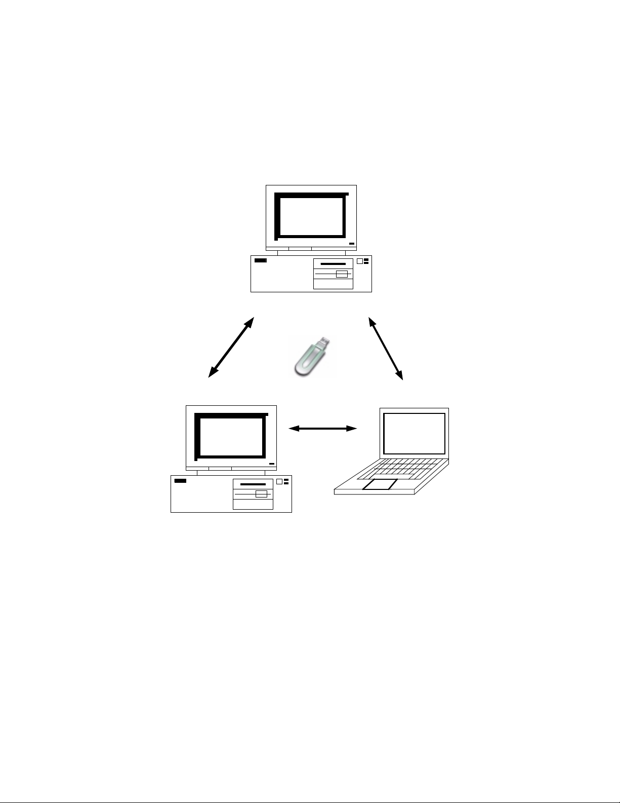
cost effective bridge between USB enabled PC and NAND type flash memory. AU9381 can
be used as a removable storage disk in enormous data exchange applications between PC,
Macintosh, laptop and workstation. It can also be configured as a bootable disk for system
repairing .
The AU9381 can work with 1 to 8 NAND type flash memory chip with the combination of
any popular flash memory type - 8M, 16M, 32M, 64M and 128M. Additional features
include write protection switch, activity LED and password protected security .
The AU9381 integrated 48MHz PLL, 3.3V regulator, power on reset circuit and a power
switch for flash memory power control.
1.2 Features
Fully compliant with USB v1.1 specification and USB Device Class Definition for
Mass Storage, Bulk-Transport v1.0
Work with default driver from Windows ME, Windows 2000, Windows XP, Mac
OS 9.1, and Mac OS X. Windows 98se is supported by vendor driver from Alcor.
Multiple FIFO implementation for concurrent bus operation
64-pin package supports to 8 pieces NAND Flash memory chip; total capacity
reaches to 2G byte when working with 1G bit mono dies chip.
48-pin package supports to 4 pieces NAND Flash memory chip; total capacity
reaches to 1G byte.
Support mixed different size NAND Flash
Vendor ID, product ID and strings can be customized by utility software from Alcor
Can be configured to support dual partitions with dynamic logic disk space
allocation.
Security function supported with password protection
LED for bus activity monitoring
Runs at 12MHz, built-in 48 MHz PLL
Built-in 3.3V regulator
Built-in power switch and power management circuit to achieve 500uA suspend
current required by USB specification.
Built-in power on reset circuit

INTRODUCTION 2
Dedicated DMA engine to ensure highest throughput in read and write
48-pin LQFP package as standard package and 64-pin LQFP package for choice.

APPLICATION BLOCK DIAGRAM 3
2.0 Application Block Diagram
Following is the application diagram of a typical flash disk product with AU9381. By
connecting the flash disk to a desktop or notebook PC through USB bus, AU9381 is
implemented as a bus-powered, full speed USB disk, which can be used as a bridge for data
transfer between Desktop PC and Notebook PC.
PC with USB Host Controller
NotebookwithUSBHost Controller

APPLICATION BLOCK DIAGRAM 4

PIN ASSIGNMENT 5
3.0 Pin Assignment
The AU9381 is packed in 48-pin LQFP form factor. The figure on the following page shows
the signal names for each of the pins on the chip. Accompanying the figure is the table that
describes each of the pin signals.
1
2
3
5
4
6
7
8
10
9
11
33
32
31
29
30
34
46 45 44 43 42
12
35
36
28
27
26
25
41 40 39 38 374748
13 14 15 16 17 18 19 20 21 22 23 24
VCCA
GNDA
XTAL1
XTAL2
VCC2FM
VCC5V
VCCIO
RSTN
USB_DP
USB_DM
GNDIO
Reserved
FMWPN
FMWRN
FMALE
FMCLE
FMCE1N
FMCE2N
FMRDN
FMRBN
GPON7
Reserved
NC
Reserved GPON6
FMCE3N
FMCE4N
VCCK
GNDK
CT3
CT4
CT2
Reserved
NC
CT1
Reserved
Reserved
FMDATA4
FMDATA5
FMDATA6
FMDATA7
FMDATA0
FMDATA1
FMDATA2
FMDATA3
Reserved
Reserved
Reserved
ALCOR MICRO
AU9381
48PIN LQFP

PIN ASSIGNMENT 6
Table 3-1. Pin Descriptions
Pin Pin Name I/O Type Description
1 VCCA PWR 3.3V input for PLL
2 GNDA PWR Ground
3 XTAL1 I Crystal Oscillator Input (12MHz)
4 XTAL2 O Crystal Oscillator Output (12MHz)
5 VCC2FM O Connect to Flash Memory VCC
6 VCC5V PWR 5V power supply
7 VCCIO PWR Regulator 3.3V output/ IO 3.3V input
8 RSTN I Hardware reset (Active Low)
9 USB_DP I/O USB D+
10 USB_DM I/O USB D-
11 GNDIO PWR Ground
12 Reserved Reserved
13 Reserved Reserved
14 FMWPN I Connect to Flash Memory Write Protect
15 FMWRN O Connect to Flash Memory Write Enable
16 FMALE O Connect to Flash Memory Address Latch Enable
17 FMCLE O Connect to Flash Memory Command Latch Enable
18 FMCE1N O Connect to Flash Memory Chip1 Enable
19 FMCE2N O Connect to Flash Memory Chip2 Enable
20 FMRDN O Connect to Flash Memory Read Enable
21 FMRBN I Connect to Flash Memory Ready/Busy Output
22 GPON7 O General Purpose Output pin, used as activity LED
23 Reserved Reserved
24 NC
25 GPON6 O Floating
26 FMCE3N O Connect to Flash Memory Chip3 Enable
27 FMCE4N O Connect to Flash Memory Chip4 Enable
28 VCCK PWR Core 3.3V Input
29 GNDK PWR Ground
30 CT3
Connect to VCC
31 CT4 Connect to ground
32 CT2 Connect to ground
33 CT1 Connect to ground
34 Reserved Connect to ground
35 Reserved Connect to ground

PIN ASSIGNMENT 7
36 NC
37 Reserved Reserved
38 FMDATA4 I/O Connect to Flash Memory Data IO4
39 FMDATA5 I/O Connect to Flash Memory Data IO5
40 FMDATA6 I/O Connect to Flash Memory Data IO6
41 FMDATA7 I/O Connect to Flash Memory Data IO7
42 FMDATA0 I/O Connect to Flash Memory Data IO0
43 FMDATA1 I/O Connect to Flash Memory Data IO1
44 FMDATA2 I/O Connect to Flash Memory Data IO2
45 FMDATA3 I/O Connect to Flash Memory Data IO3
46 Reserved Reserved
47 Reserved Reserved
48 Reserved
Reserved

SYSTEM ARCHITECTURE AND REFERENCE DESIGN 8

SYSTEM ARCHITECTURE AND REFERENCE DESIGN 9
4.0 System Architecture and
Reference Design
4.1 AU9381 Block Diagram
Alcor Micro - AU9381 Flash Memory Card Reader Block Diagram
FM control
& FIFO
USB
SIE
USB
Upstream
Port
XCVR
USB
FIFO
3.3 V
Voltage
Regulator
& Power off
3.3 V
RAM
Processor ROM
12MHz
XTAL
Support up to 8
Flash Memory
Suspend

SYSTEM ARCHITECTURE AND REFERENCE DESIGN 10
4.2 Sample Schematics
FMRDN GNDK
C4
0.1UF
R1
1.5K R2 39
FMIO[0..7]
GPON7
FMCE1N
VCCK
C7
0.1UF
VCC
GPON7
GNDA
C5 18PF R5
1M
FMWRN
XTAL2
Y1
12MHZ
VCC3.3
XTAL1
FMCE3N
VCC2FM
XTAL2
C8
0.1UF
VCC2FM
FMALE
A
12Wednesday, April 02, 2003
1.00
Au9381 4 flash memory demostration schematic
Size Document Number Rev
Date: Sheet of
FMRBN
R3 39
C3
1UF
U1
Au9381-48 pin
1
2
3
4
5
6
7
8
9
10
11
13
14
15
16
17
18
19
20
21
22
23 25
26
27
28
29
30
31
32
33
34
35
37
38
39
40
41
42
43
44
45
46
47
12
24
36
48
VCCA
GNDA
XTAL1
XTAL2
VCC2FM
VCC5V
VCCIO
RSTN
USB_DP
USB_DM
GNDIO
RESERVED
FMWPN
FMWRN
FMALE
FMCLE
FMCE1N
FNCE2N
FMRDN
FMRBN
GPON7
RESERVED GPON6
FMCE3N
FMCE4N
VCCK
GNDK
RESERVED
RESERVED
RESERVED
RESERVED
RESERVED
RESERVED
RESERVED
FMIO4
FMIO5
FMIO6
FMIO7
FMIO0
FMIO1
FMIO2
FMIO3
RESERVED
RESERVED
RESERVED
RESERVED
RESERVED
RESERVED
F1
FB
VCC3.3
GNDK
J1 1
2
3
4
5
VCC
DATA-
DATA+
GND
FGND1
Disclaimer: This schematic is for reference only.
Alcor Micro Corp. makes no warranty for the use of its
products and bears no responsibility for any error that
appear in this document. Specifications are subject to
change without notice.
D1
FMCE2N
VCC3.3 GNDA
VCCA
VCC5V
R4
47K
C6 18PF
VCC5V
C9
0.1UF
SW1
2
1
3
R6 330
C2
10UF
VCCA VCCK
VCC3.3
F2FB
FMCE4N
VCC
FMCLE
C1
0.1UF
XTAL1
VCC3.3
VCC3.3

ELECTRICAL CHARACTERISTICS 11
FMIO5
FMCLE
FMWRN
FMCE2N
FMIO0
FMIO3
FMIO3
VCC2FM
FMRBN
CB2
0.1UF
FMIO7
FMALE
FMIO1
FMIO6
FMIO1
FMCLE
FMIO1 FMIO0
FMIO4
FMIO2
FMIO[0..7]
VCC2FM
FMALE
FMCE2N
FMIO4
CB1
0.1UF
FMIO5
FMIO1
FMRBN
FMALE
VCC2FM
CB4
0.1UF
FMIO3
A
22Wednesday, April 02, 2003
1.00
Au9381 4 flash memory demostration schematic
Size Document Number Rev
Date: Sheet of
FMIO4
FMWRN
CB3
0.1UF
U2
K9F5608U0A-YCB0
29
30
31
32
41
42
43
44
6
13
36
12
37
7
8
9
16
17
18
19
I/O0
I/O1
I/O2
I/O3
I/O4
I/O5
I/O6
I/O7
GND
VSS
VSS
VCC
VCC
R/B
RE
CE
CLE
ALE
WE
WP
FMIO4
FMIO2
U3
K9F5608U0A-YCB0
29
30
31
32
41
42
43
44
6
13
36
12
37
7
8
9
16
17
18
19
I/O0
I/O1
I/O2
I/O3
I/O4
I/O5
I/O6
I/O7
GND
VSS
VSS
VCC
VCC
R/B
RE
CE
CLE
ALE
WE
WP
FMIO6
FMIO6
VCC2FM
FMIO6
FMWRN
FMCE1N
FMIO0
FMIO3
FMRDN
FMCLE
FMRDN
U5
K9F5608U0A-YCB0
29
30
31
32
41
42
43
44
6
13
36
12
37
7
8
9
16
17
18
19
I/O0
I/O1
I/O2
I/O3
I/O4
I/O5
I/O6
I/O7
GND
VSS
VSS
VCC
VCC
R/B
RE
CE
CLE
ALE
WE
WP
FMRDN
FMCE1N
VCC2FM
FMIO5
FMIO5
FMIO7
U4
K9F5608U0A-YCB0
29
30
31
32
41
42
43
44
6
13
36
12
37
7
8
9
16
17
18
19
I/O0
I/O1
I/O2
I/O3
I/O4
I/O5
I/O6
I/O7
GND
VSS
VSS
VCC
VCC
R/B
RE
CE
CLE
ALE
WE
WP
FMIO7
FMIO2
VCC2FM
FMRBN
FMRBN
Disclaimer: This schematic is for reference only.
Alcor Micro Corp. makes no warranty for the use of its
products and bears no responsibility for any error that
appear in this document. Specifications are subject to
change without notice.
FMRDN
FMALE
FMIO7
VCC2FM
FMIO2
FMWRN
FMIO0
FMCLE
VCC2FM

ELECTRICAL CHARACTERISTICS 12

ELECTRICAL CHARACTERISTICS 13
5.0 Electrical Characteristics
5.1Recommended Operating Conditions
SYMBOL PARAMETER MIN TYP MAX UNITS
VCC Power Supply 4.75 5 5.25 V
VIN Input Voltage 0 VCC V
TOPR Operating Temperature 0 85 OC
TSTG Storage Temperature -40 125
OC
5.2General DC Characteristics
SYMBOL PARAMETER CONDITIONS MIN TYP MAX UNITS
IIL Input low current no pull-up or pull-down -1 1 µA
IIH Input high current no pull-up or pull-down -1 1 µA
IOZ Tri-state leakage current -10 10 µA
CIN Input capacitance 5 ρF
COUT Output capacitance 5 ρF
CBID Bi-directional buffer capacitance 5 ρF
5.3 DC Electrical Characteristics for 3.3 volts operation
SYMBO
L
PARAMETER CONDITIONS MIN TYP MAX UNITS
VIL Input Low Voltage CMOS 0.9 V
VIH Input Hight Voltage CMOS 2.3 V
VOL Output low voltage IOL=4mA, 16mA 0.4 V
VOH Output high voltage IOH=4mA,16mA 2.4 V
RIInput Pull-up/down resistance Vil=0V or Vih=VCC 10k/200k KΩ

ELECTRICAL CHARACTERISTICS 14
5.4 Crystal Oscillator Circuit Setup for Characterization
The following setup was used to measure the open loop voltage gain for crystal oscillator
circuits. The feedback resistor serves to bias the circuit at its quiescent operating point and
the AC coupling capacitor, Cs, is much larger than C1 and C2.

ELECTRICAL CHARACTERISTICS 15
5.5 ESD Test Results
Test Description : ESD Testing was performed on a Zapmaster system using the Human-
Body –Model (HBM) and Machine-Model (MM), according to MIL_STD 883 and EIAJ
IC_121 respectively.
Human-Body-Model stress devices by sudden application of a high voltage supplied
by a 100 PF capacitor through 1.5 Kohm resistance.
Machine-Model stresses devices by sudden application of a high voltage supplied by a
200 PF capacitor through very low (0 ohm) resistance
Test circuit & condition
Zap Interval : 1 second
Number of Zaps : 3 positive and 3 negative at room temperature
Critera : I-V Curve Tracing
Model Model S/S TARGET Results
HBM Vdd, Vss, I/C 15 4000V Pass
MM Vdd, Vss, I/C 15 200V Pass

ELECTRICAL CHARACTERISTICS 16
5.6 Latch-Up Test Results
Test Description: Latch-Up testing was performed at room ambient using an
IMCS-4600 system which applies a stepped voltage to one pin per device with
all other pins open except Vdd and Vss which were biased to 5 Volts and
ground respectively.
Testing was started at 5.0 V (Positive) or 0 V(Negative), and the DUT was
biased for 0.5 seconds.
If neither the PUT current supply nor the device current supply reached the
predefined limit (DUT=0 mA , Icc=100 mA), then the voltage was increased
by 0.1 Volts and the pin was tested again.
This procedure was recommended by the JEDEC JC-40.2 CMOS Logic
standardization committee.
Notes:
1. DUT: Device Under Test.
2. PUT: Pin Under Test.
Vcc
DUT
GND
Pin
under
m
Untested
Output Open
Circuit
Untested
Input Tied
to V supply
Trigger
Sou
r
ce
V Su
pp
l
y
+
+
Icc Measurement
1 Source
Test Circuit : Positive Input/ output Overvoltage /Overcurrent
Table of contents
Other Alcor Controllers manuals