D R - 235T M k I I I
S e r v ic e M a n u a l
C O N T E N T S
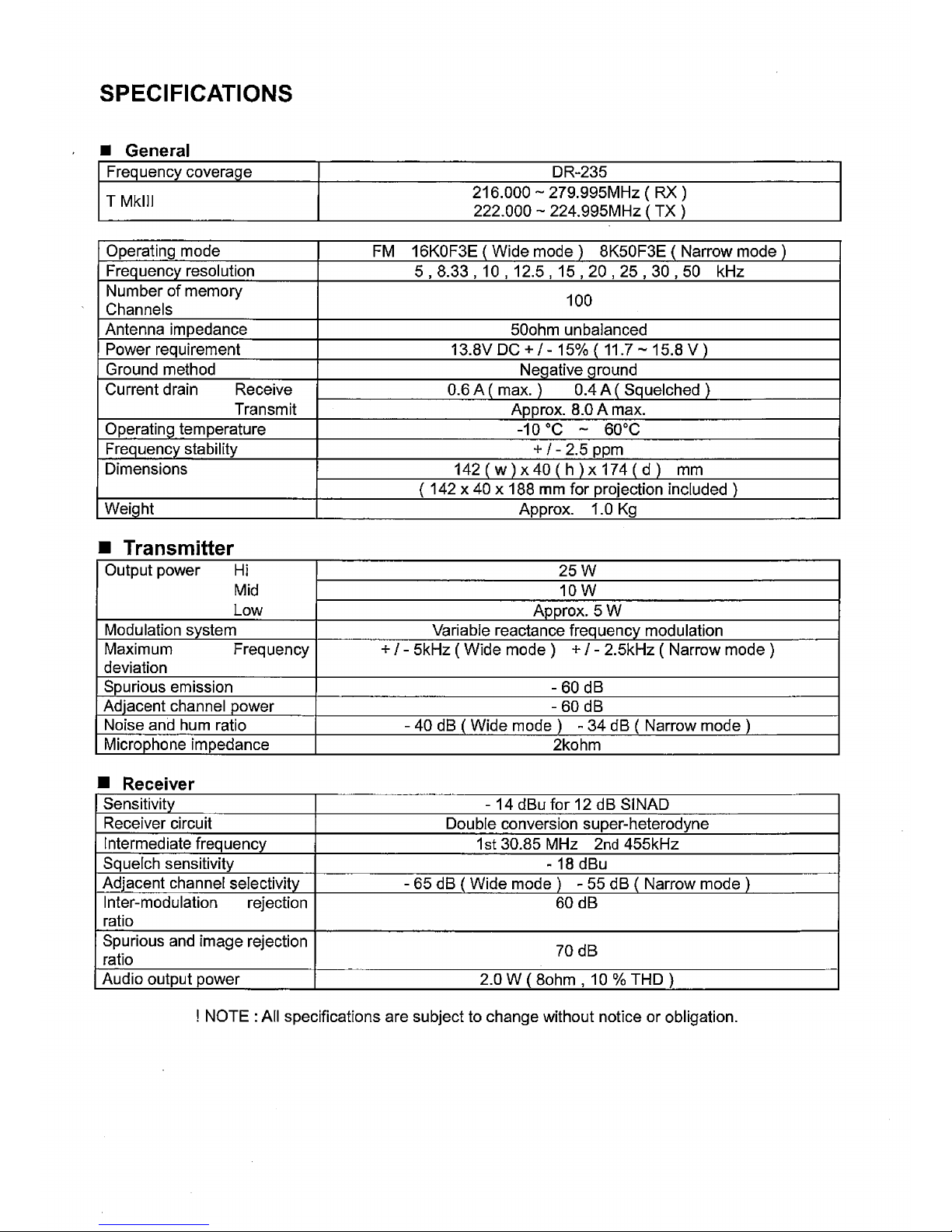
SPECIFICATIONS
GENERAL
.........................................................
TRANSMITTER................................................
RECEIVER........................................................
CIRC IT D IS C R E TIO N
1) Receiver System DR-235................................
2) Transmitter System DR-235
............................
3) PLL Synthesizer Circuit DR-235......................
4) CP and Peripheral Circuit..............................
5) Power Supply Circuit
.......................................
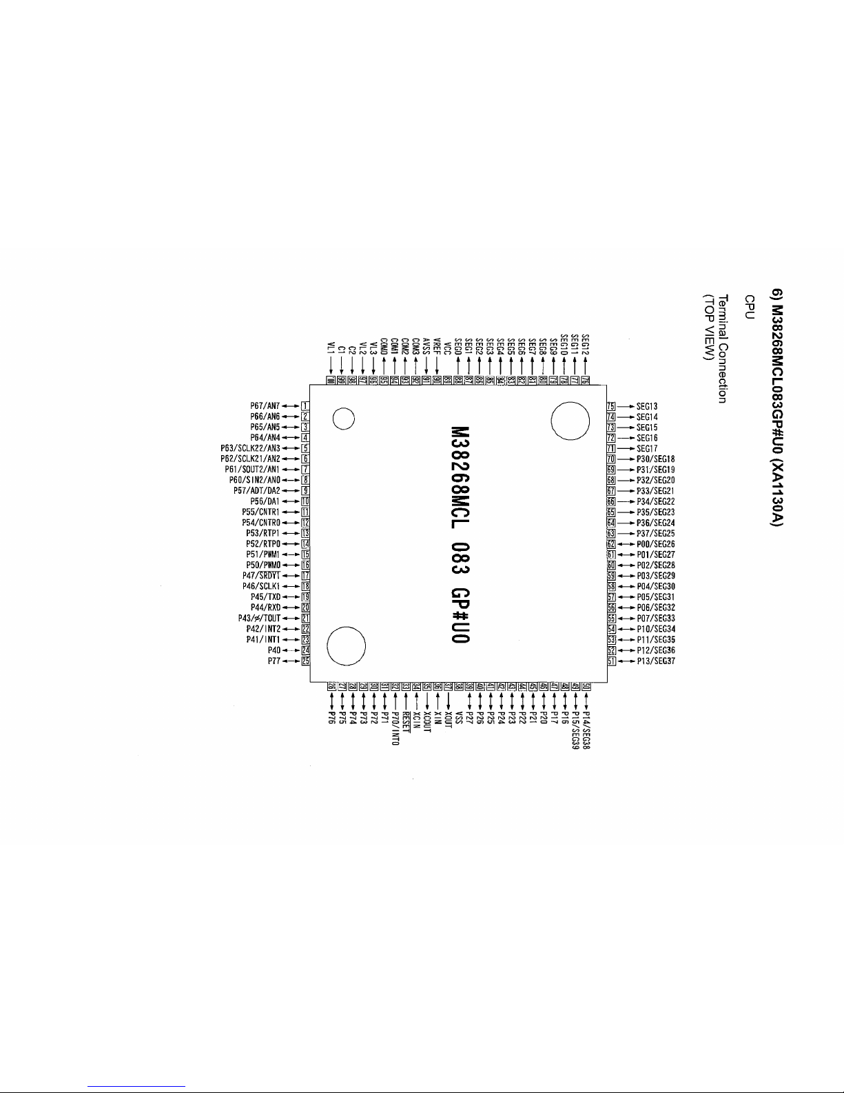
6) M38268MCA075GP (XA1130).........................
SEM ICO N D C TO R DATA
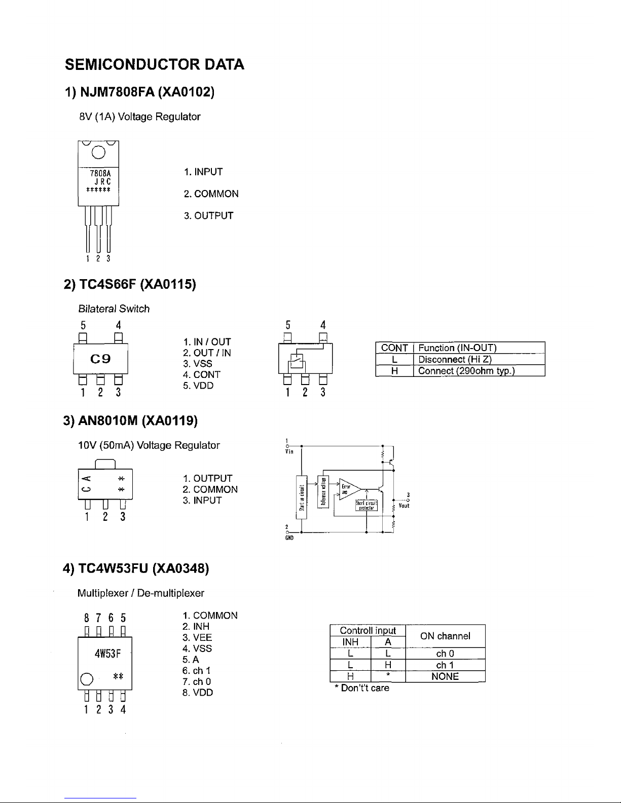
1) NJM7808FA (XA0102)
.....................................
2) TC4S66F (XA0115)
..........................................
3) AN8010M (XA0119).........................................
4) TC4W53F (XA0348)
......................................
5) TA31136FN (XA0404)
......................................
6) LA4425A (XA0410)
..........................................
7) BR24L32FJ (XA0604Z)
...................................
8) L88MS05TLL (XA0675)....................................
9) S-816A50AMC (XA0925)
.................................
10) LM2904PWR (XA1103)
...................................
11) LM2902PWR (XA1106)
...................................
12) MB15E07SR (XA1107).....................................
13) S-80845CLNB (XA1120)
.................................
14) B 4052BCFV (XA1229)
.................................
15) S-AV40 (XA1230).............................................
16) Transistor, Diode and LED Outline Drawing...
17) LCD Connection (TTR3626 PFDHN)............
EXPLODED VIEW
1) LCD Assembly..................................................
2) Top and Front View
..........................................
3) Bottom View......................................................
PARTS LIST
2 CP nit
...................................................
21,22
2 MAIN nit................................................ 22-25
2 Mechanical Parts
..................................... 25
Packing Parts........................................... 25
ACCESSORIES...................................... 25
3,4 ACCESSORIES (SCREW SET)............. 25
4 TNC (EJ41 )............................................ 26
5 TNC (EJ41 ) Packing Parts
...................
27
5 6 ^
6 DR-235 ADJ STMENT
7-9 1) Adjustment Spot
..................................... 28
2) VCO and RX Adjustment Specification.. 29
3) TX Adjustment Specification
..................
30
10 4) RX Test Specification
.............................
31
10 5) TX Test Specification
.............................
32
10
10 PC BOARD VIEW
11 1) CP nit Side A DR-235 ( P0579)
......
33
2) CP nit Side B DR-235 ( P0579)
......
33
11 3) MAIN nit Side A DR-235 ( P0579)
.....
34
12 4) MAIN nit Side B DR-235 ( P0579).... 34
12 5) TNC nit Side A ( P0402) (option)
......
35
12 6) TNC nit Side B ( P0402) (option)
.....
35
12
13 SCHEMATIC DIAGRAM
14 1) CP nit DR-235
...................................
36
14 2) MAIN nit DR-235.................................. 37
15 3) TNC nit (option).................................... 38
16
17 BLOCK DIAGRAM
1) DR-235.................................................... 39
18
19
20
A U N C O , I N C