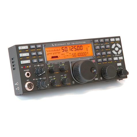
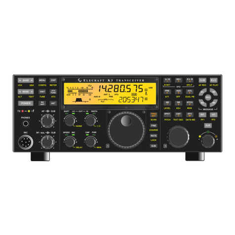
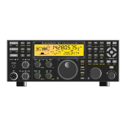
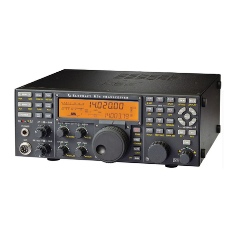
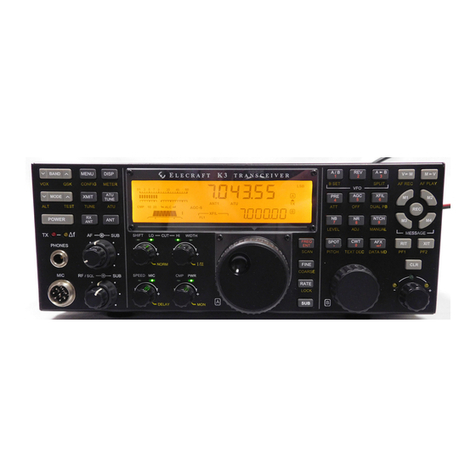
ELECRAFT K2/100 User manual

1
Appendix G, 100-W Stage and RS-232 I/O (K2/100) Rev H3, July 24, 2017
E740035

2
Table of Contents
Introduction..........................................................................................................................................................................................3
Customer Service Information .............................................................................................................................................................4
Parts Inventory.....................................................................................................................................................................................5
Assembly, Part I.................................................................................................................................................................................13
Initial Tests.........................................................................................................................................................................................23
Assembly, Part II................................................................................................................................................................................28
Alignment and Installation..................................................................................................................................................................45
Using the K2/100 at High Power........................................................................................................................................................57
Remote Control using the RS-232 Port .............................................................................................................................................60
K2/100 Specifications........................................................................................................................................................................65
Troubleshooting and Repair ..............................................................................................................................................................66
Circuit Details.....................................................................................................................................................................................70
Schematic Diagrams..........................................................................................................................................................................71
Parts Placement Drawings.................................................................................................................................................................73
i
Elecraft manuals with color images may be downloaded from www.elecraft.com.

3
Introduction
Appendix G describes assembly of the K2/100 transceiver's internal 100-
watt final output stage (KPA100 board). The PC board includes two
conservatively-rated RF power transistors, low-pass filters, SWR bridge,
monitoring circuits, speaker, and an RS-232 interface. Filter switching, T-
R sequencing, and other configuration is handled by the K2/100's main
microcontroller.
KPA100 assembly and installation should be done only after the
transceiver has been aligned and tested at the 10-watt level.
Upgrades Recommended for Older K2s
All K2 owners are encouraged to keep their transceivers up to date by
making recommended changes. These changes should be installed and
tested before the KPA100 is installed.
K2 s/n 4059 or lower: K2 keying bandwidth modification (order
#K2KEYMODKT). This modification is strongly recommended for CW
operators, especially if you use high power. Note: Requires upgrade to
revision 2.04 or later K2 firmware (order #FWK2MCIO).
K2 s/n 3445 or lower: PLL Upgrade (order #E850138). This ensures
excellent VFO temperature stability during high-power operation.
K2 s/n 2999 or lower: (1) 10 meter band-pass filter and VFO ALC
modification (#E850093, supplied with your KPA100 kit). (2) BFO
modification (order #BFOMDKT). You should also make all applicable
changes described in this document:
http://www.elecraft.com/manual/k2a2binstr.pdf
Pre-Wound Toroids Available
The toroids used in the KPA100 are not difficult to wind, and full
instructions are provided. If you prefer not to wind them yourself, you
can obtain a full set of pre-wound toroids from an Elecraft-qualified
source. Ordering information can be found on our web site,
www.elecraft.com. You do not need to send your cores or wire to the
winding service.
Preparation for Assembly
With all equipment that operates at high power levels, proper assembly
and alignment are critical for safe and reliable operation. Follow the
instructions carefully and make all of the recommended measurements.
Do not substitute components or perform any assembly steps out of order.
Please read the following information regarding tools before
proceeding.
Tools Required
The following tools are required to build this kit:
Flush-cutters (Hakko CHP-170, Xcelite 170, etc.). Ordinary
diagonal cutters are not suitable for flush-cutting (trimming leads
very close to the board).
Temperature-controlled soldering station with a fine-point, 700
to 800-degree (F) tip. Do not use a high-wattage iron or gun with
small components, since this can damage pads, traces, or the parts
themselves.
Larger iron or soldering gun. This will be used only for installation
of power transistors, output transformer, and DC power wiring. A
low-wattage iron cannot be used for these steps.
Digital Multimeter (DMM). A DMM with diode-checking
capability. Capacitance measurement capability is desirable, though
not required.

4
Customer Service Information
Technical Assistance
quickly - typically the same day Monday through Friday. Telephone
assistance is available from 9 A.M. to 5 P.M. Pacific time (weekdays
only) at 831-763-4211. Please use e-mail rather than calling when
possible since this gives us a written record of the details of your problem
and allows us to handle a larger number of requests each day.
Repair / Alignment Service (We want to make sure everyone
succeeds!)
If necessary, you may return your Elecraft product to us for repair or
alignment. (Note: We offer unlimited email and phone support to get
your kit running, so please try that route first as we can usually help you
find the problem quickly.)
IMPORTANT: You must contact Elecraft before mailing your
product to obtain authorization for the return, what address to ship it to
and current information on repair fees and turnaround times. (Frequently
we can determine the cause of your problem and save you the trouble of
shipping it back to us.) Our repair location is different from our factory
location. We will give you the address to ship your kit to at the time of
repair authorization. Packages shipped us without authorization will
incur an additional shipping charge for reshipment to our repair depot.
To ship the unit, first seal it in a plastic bag to protect the finish. Use a
sturdy packing carton with at least 3-in (8 cm) of foam or shredded paper
on all sides. Seal the package with reinforced tape. (Neither Elecraft or
the carrier will accept liability for damage due to improper packaging.)
Elecraft's 1-Year Limited Warranty
This warranty is effective as of the date of first consumer purchase (or if shipped
from factory, date product is shipped to customer). It covers both our kits and
fully assembled products. For kits, before requesting warranty service, you
should fully complete the assembly, carefully following all instructions in the
manual.
Who is covered: This warranty covers the original owner of the Elecraft
product as disclosed to Elecraft at the time of order. Elecraft products
transferred by the purchaser to a third party, either by sale, gift or other method,
who is not disclosed to Elecraft at the time of original order, are not covered by
this warranty. If the Elecraft product is being bought indirectly for a third party,
the third party's name and address must be provided to Elecraft at time of order
to insure warranty coverage.
What is covered: During the first year after date of purchase, Elecraft will
replace defective or missing parts free of charge (post-paid). We will also
correct any malfunction to kits or assembled units caused by defective parts and
materials. Purchaser pays inbound shipping to Elecraft for warranty repair,
Elecraft will pay shipping to return the repaired equipment to you by UPS
ground service or equivalent to the continental USA and Canada. Alaska, Hawaii
and outside U.S. and Canada actual return shipping cost paid by owner.
What is not covered: This warranty does not cover correction of kit assembly
errors. It also does not cover misalignment; repair of damage caused by misuse,
negligence, or builder modifications; or any performance malfunctions involving
non-Elecraft accessory equipment. The use of acid-core solder, water-soluble
flux solder, or any corrosive or conductive flux or solvent will void this warranty
in its entirety. Also not covered is reimbursement for loss of use, inconvenience,
customer assembly or alignment time, or cost of unauthorized service.
Limitation of incidental or consequential damages: This warranty does not
extend to non-Elecraft equipment or components used in conjunction with our
products. Any such repair or replacement is the responsibility of the customer.
Elecraft will not be liable for any special, indirect, incidental or consequential
damages, including but not limited to any loss of business or profits.

5
Parts Inventory
Set the heat sink, shield, and painted panels aside until needed. Leave them wrapped to protect their finish.
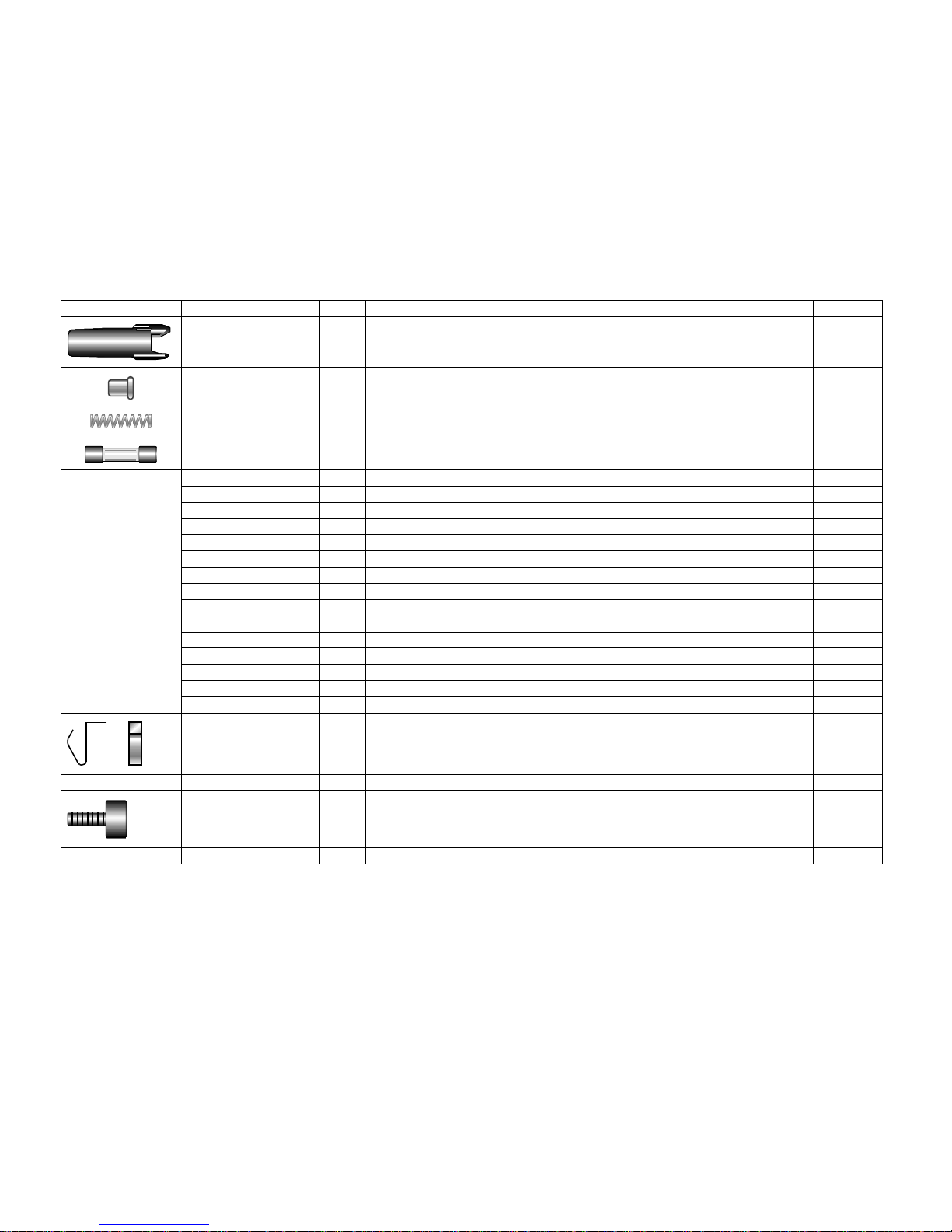
You should do a complete inventory (see below), which may take an hour or more. If anything is missing, contact Elecraft. Color codes and other
markings are shown in parentheses. Refer to Appendix A of the owner's manual for more parts photos.
Some components in this kit can be damaged by static discharge. Before handling diodes, transistors, and ICs, touch a grounded, unpainted metal
surface, or use a wrist strap.
Parts List Notes:
LS = lead spacing in inches (metric conversions: 0.1" = 2.5 mm, 0.2" = 5 mm, 0.4" = 10 mm.)
In some cases, two capacitor types will have the same value but different voltage ratings or lead spacing (LS). To avoid assembly errors, you
must positively identify these capacitors and keep them separate from each other. Use your DMM to verify values if possible.
Parts whose reference designators are shown in bold are for use on the K2 RF or Control boards.
Flat-head screws are measured from the top of the head; pan head screws are measured from beneath the head.
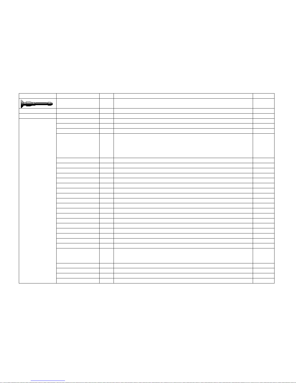
Picture
Ref. Designator(s)

QTY
Description
Part #
C5B
1
Cap., 18 pF ("18"), 5%, 500V or 1KV disc, 0.2" LS (may have black band)
E530088
C3B,C4B
2
Cap., 27 pF ("27"), 5%, 500V or 1KV disc, 0.2" LS
E530089
C5F
1
Cap., 33 pF ("33"), 5%, 500V or 1KV disc, 0.2" LS
E530090
C3H
1
Cap., 39 pF ("39"), 5%, 500V or 1KV disc, 0.2" LS
E530091
C5D
1
Cap., 47 pF ("47"), 5%, 500V or 1KV disc, 0.2" LS
E530092
C4D
1
Cap., 56 pF ("56"), 5%, 500V or 1KV disc, 0.2" LS (may have black band)
E530093
C5A,C6C
2
Cap., 68 pF ("68"), 5%, 500V or 1KV disc, 0.2" LS
E530094
C3E,C5G
2
Cap., 82 pF ("82"), 5%, 500V or 1KV disc, 0.2" LS
E530095
C4E
1
Cap., 120 pF ("121"), 5%, 500V or 1KV disc, 0.2" LS
E530096
C3G,C4A,C5C,C5E,
C6E
5
Cap., 150 pF ("151"), 5%, 500V or 1KV disc, 0.2" LS
E530097
C2B,C3C,C3J
3
Cap., 220 pF ("221"), 5%, 500V or 1KV disc, 0.2" LS
E530098
C3A,C3D,C4C,C6F
4
Cap., 270 pF ("271"), 5%, 500V or 1KV disc, 0.2" LS
E530099
C3F,C6A,C6B,C6G
4
Cap., 330 pF ("331"), 5%, 500V or 1KV disc, 0.2" LS
E530100
C2D
1
Cap., 390 pF ("391"), 5%, 500V or 1KV disc, 0.2" LS
E530101
C26
1
Cap., 33 pF ("33"), 5%, 50V disc, 0.2" LS (do not confuse with C5F)
E530064
C41,C95
2
Cap., 100 pF ("101"), 5%, 200V disc, 0.2" LS
E530034

6
Picture
Ref. Designator(s)
QTY
Description
Part #
C66
1
Cap., 180 pF ("181"), 5%, 50V disc, 0.2" LS; voltage may not be marked
E530008
C67,C80,C81,C86
4
Cap., .0047 µF ("472"), 10%, 100V disc, 0.25" LS
E530102
C2E,C83
2
Cap., 1000 pF ("1000"), 5%, 500V silver mica
E530085
C2A,C6D
2
Cap., 1200 pF ("6122"), 630V polypropylene
E530033
C2C
1
Cap., 2200 pF ("2200"), 5%, 500V silver mica
E530086
C84
1
Cap., .001 µF ("102"), 5%, 50V mono, 0.1" LS
E530074
C25,C69,C70,C87,
C88, CTRL-Ctxd
6
Cap., .001 µF ("102"), 5%, 50V mono, 0.2" LS
(CTRL-Ctxd may be needed for K2 Control board; see text)
E530001
C82
0
Not used
-
C71
1
Cap., .0018 µF ("182"), 5%, 200V mono, 0.2" LS
E530104
C64, C79
2
Cap., .0047 µF ("4n7J250"), 5%, 250Vor greater, mono, 0.4" LS
E530262
C7,C8,C9,C12–C22,
C24,C28,C29,C32,
C50,C65,C72,C73,
C74,C76,C97–C99
27
Cap., .01 µF ("103"), 5%, 50V mono, 0.1" LS
E530019
C37,C38,C39,C44,
C46,C68,C89,C90
8
Cap., .01 µF ("103"), 5%, 50V mono, 0.2" LS
E530009
C36,C42,C43,C77
4
Cap., .015 µF ("153" or "15N"), 5%, 250V mono, 0.2" LS
E530082
C31
1
Cap., .22 µF ("µ22J63"), 5%, 63V mono, 0.2" LS
E530295
C48,C49,C52,C53,
C54,C55,C56,C57,
C61,C62,C63,C85
RF-Crf
13
Cap., .047 µF ("473"), 5%, 50V mono, 0.2" LS
(RF-Crf may be needed for the K2 RF board; see text)
E530025
C30,C33,C34,C75
4
Cap., 0.1 µF ("104"), 20%, 50V mono, 0.1" LS
E530020
C10,C11,C23,C35,
C58,C59,C40,
CTRL-C42
8
Cap., 0.1 µF ("104"), 5%, 50V mono, 0.2" LS
(CTRL-C42 may be needed for the K2 Control board; see text)
E530011
C27
1
Cap., 10-50 pF ceramic trimmer, yellow color
E540002
C1
1
Cap 3-11 ceramic trimmer, white color:
NOTE: This trimmer is packaged in a separate envelope to help you avoid
confusing it with C27. Keep it in its envelope until you are instructed to
install it.
E540012
C60
1
Cap., 100 µF, 16V electrolytic
E530061
C51
1
Cap., 470 µF, 25V electrolytic
E530084
D1-D8
8
Diode, 1N4148
E560002
D9
1
Diode, SB530
E560003
D10,D13
2
Diode, 1N5404
E560010
D11,D12,D14
3
Diode, 1N4007
E560001

7
Picture
Ref. Designator(s)
QTY
Description
Part #
D16,D17
2
Diode, 1N5711
E560004
E1
1
Ground terminal, right angle PCB mount, 6-32 threaded
E700012
FAN1
1
Fan, 12 V
E980046
J2
1
Connector, SO239 (Antenna)
E620064
J3, P3
2
Connector, DC power, red housing (13.8 VDC input and mating conn., +)
E620059
J3, P3
2
Connector, DC power, black housing (13.8 VDC input and mating conn., -)
E620060
MISC
2
PCB pin for J3, 25 amp right angle
E620061
MISC
2
Crimp/solder terminal for P3, 30 amps
E620062
HDWR
2
Mounting plate for J3
E620063
MISC
1
Spring pin, 3/32" x 1/4" (2.4 x 6.4 mm); stabilizing pin for P3
E700071
J1,J4
2
Connector, 2p female housing, 0.156" spacing (12V and RF connectors)
E620013
RF-P3, RF-P6
2
Mating connectors for J1 and J4, 2p male, 0.156" spacing (K2 RF board)
E620012
HDWR
5
Crimp/solder terminal for J1 and J4, gold color (1 spare)
E620014
J5
1
Connector, 2p female housing, 0.1" spacing (AF In)
E620021
HDWR
3
Crimp/solder terminal for J5 (1 spare)
E620022
J6
1
Connector, 1/8" mono jack w/switch, PCB mount (ext. speaker)
E620056
J7
1
Connector, RCA jack, PCB mount (ext. PA key)
E620057
J8
1
Connector, DB9F, PCB mount (RS-232 interface)
E620058

8
Picture
Ref. Designator(s)
QTY
Description
Part #
MISC
2
Keying insert for ribbon cable connector
(Shown approx. 4x actual size; may include large break-away tab)
E700065
MISC
1
Connector, DB9M (serial I/O cable, K2 end)
E620049
MISC
1
Connector, DB9F (serial I/O cable, PC end)
E620048
MISC
2
Backshell for serial I/O cable
E620050
K1-K12
12
Relay, SPDT, 12 V
E640011
L1,L2,L13,L14
4
Toroidal ind., T50-2 core (iron powder, red, 0.5" dia.)
E680005
L4-L8,L10-L12
8
Toroidal ind., T50-10 core (iron powder, black, 0.5" dia.)
Note: One FT50-43 gray ferrite core, also 0.5" dia,, is supplied (see T4).
The T50-10 iron power cores have a shiny, black finish, while the
ferrite core is dull gray. Label the ferrite core to avoid confusing it with the
eight iron powder cores.
E680016
L16, RFC1
2
Toroidal ind., T50-1 core (iron powder, blue, 0.5" dia.)
E680001
L18
0
Jumper (see text)
n/a
P1
1
Connector, 10 pin dual row (5 x 2), 0.1" spacing
E620040
Q1,Q2
1
Matched set of (2) 2SC2879 transistors
E850123
Q3,Q4
2
Transistor, NPN, MJE182, TO-225AA package
E580016
Q5,Q8
2
Transistor, NPN, 2N3904, TO-92
E580017
Q6,Q7
2
Transistor, MOSFET, 200 V, ZVN4424, TO-92
E580005
Q10,Q11,Q12
3
Transistor, MOSFET, 60 V, 2N7000, TO-92
E580002
Q9
1
Transistor, HEXFET, 500 V, IRF830 or IRL620, TO-220 (tab may be cut)
E580018
R2,R3
2
Resistor, 2.7 ohms, 5%, 1/4 W (RED-VIO-GOLD)
E500055
R9
1
Resistor, 10 ohms, 5%, 1/4 W (BRN-BLK-BLK)
E500054
R10
1
Resistor, 47, 5%, 1/4 W (YEL-VIO-BLK)
E500019
R33
1
Resistor, 1000 ohms, 5%, 1/4W (BRN-BLK-RED)
E500013
R1,R29,R15,R16
4
Resistor, 3.3 k, 5%, 1/4 W (ORG-ORG-RED)
E500017
R8
1
Resistor, 10 k, 5%, 1/4 W (BRN-BLK-ORG)
E500015
R5
1
Resistor, 15 k, 5%, 1/4 W (BRN-GRN-ORG)
E500060
R4
1
Resistor, 100k, 5%, 1/4W (BRN-BLK-YEL)
E500006
R11
1
Resistor, 510 k, 5%, 1/4W (GRN-BRN-YEL)
E500069
R32
1
Resistor, 100 ohms, 1%, 1/4W (BRN-BLK-BLK-BLK)
Note: Don't confuse R32 with 100-µH RF choke RFC3. RF chokes can be
identified by their much lower DC resistance (typically 1 to 8 ohms).
E500059
R30
1
Resistor, 3.09 k, 1%, 1/4W (ORG-BLK-WHT-BRN)
E500072
R24,R25
2
Resistor, 8.45 k, 1%, 1/4W (GRY-YEL-GRN-BRN)
E500071
R28,R31
2
Resistor, 200 ohms, 5%, 1W (RED-BLK-BRN) or (201J)
E500074
R40
1
Resistor, 22K, 5%, 1/4W (RED-RED-ORG)
E500090

9
Picture
Ref. Designator(s)
QTY
Description
Part #
R23
0
Resistor, 0 ohms (jumper); see text
n/a
R14
1
Resistor, 470 ohms, 5%, 1W (YEL-VIO-BRN)
E500075
R19,R20
2
Resistor, 1.6 ohms, 5%, 2W
E500177
R21,R34,R35
3
Resistor, 10 ohms, 5%, 2W
E500077
R38,R39
2
Resistor, 22 ohms, 5%, 3W
E500128
R22
1
Resistor, 300 ohms, 5%, 2W
E500129
R13
1
Resistor, 100 ohms, 5%, 3W
E500080
R7
1
Resistor, .005 ohms, 1%, 3W (current sensing)
E500079
R6
1
Potentiometer, 1K trimmer ("102"), bias set
E520010
R26,R27
2
Potentiometer, 100K trimmer ("104"), SWR set
E520001
RFC3,RFC11
2
RF Choke, 100 µH (BRN-BLK-BRN), 0.4" LS
E690016
RFC4, RFC5, RFC9
3
RF Choke, 15 µH (BRN-GRN-BLK), 0.4” LS
E690006
RFC6,RFC7,RFC8
3
RF Choke, 100 µH, miniature (BRN-BLK-BRN), 0.2" LS
E680013
RP1
1
Resistor network, 3.9 k, 8 pins (marked part number should include "392")
E510000
SP1
1
Speaker, 4 ohms, 3W
E980007
T1
1
Transformer, small binocular toroid core (gray, approx. 0.5" x 0.75")
E680014
T2
1
Transformer, large binocular toroid core (gray, approx. 1" x 1.2")
E680015
T3
1
Transformer, FT37-61 toroidal core (gray, 0.37" dia.)
E680002
T4
1
Transformer, FT50-43 toroidal core (gray, 0.5" dia.)
E680008
U1
1
IC, PIC16F872 microcontroller, pre-programmed, KPA100
E610011
MISC
1
Socket for U1, 28 pins
E620011
U2
1
IC, octal peripheral driver, TD62083AP (alt: ULN2803)
E600040
U3
1
IC, 5-volt regulator, 78L05
E600029
U4
1
IC, RS-232 driver/receiver, MAX1406CPE (alt: LT1039CN16)
E600036
U5
1
IC, dual op-amp, LM358AN
E600010
U6
1
IC, high-current op-amp w/enable, EL5146CN
E600041
U7
1
IC, dual op-amp, rail-to-rail, LMC6482AIN
E600011
X1
1
Crystal, 18.432 MHz, low profile ("S184ECSL")
E660019
X2
1
Crystal, 4 MHz ("4.00-20")
E660006
Z1
2
Ferrite beads, 0.23" (6 mm) long; two beads on a 1N4007 diode lead)
E980029

10
Picture
Ref. Designator(s)
QTY
Description
Part #
HDWR
2
Fuse holder housing, twist-lock (for external 20A fuse)
E980047
HDWR
2
Fuse holder contacts, #12 size
E980048
HDWR
1
Fuse holder spring, for 1.25" long fuse
E980049
HDWR
2
Fuse, 20A, Littlefuse #312020 or equivalent (1 spare)
E980050
HDWR
2
Jackscrew, 4-40, hex (for J8)
E700078
HDWR
5
Standoff, 3/16 dia. x 3/16" long hex 4-40 thd (between PCB and heat sink)
E700068
HDWR
2
Standoff, 3/16 dia. x 1/2" long hex 4-40 thd (between PCB and shield)
E700061
HDWR
5
Standoff, 3/16 dia. x 5/8" long hex 4-40 thd (between PCB and shield)
E700060
HDWR
20
Screw, 4-40 x 3/16" pan head, black oxide (2 spares)
E700015
HDWR
5
Screw, 4-40 x 3/16" undercut flathead, black oxide (1 spare)
E700025
HDWR
19
Screw, 4-40 x 1/4" panhead (2 spares)
E700005
HDWR
3
Screw, 4-40 x 1/4" flathead (1 spare)
E700063
HDWR
5
Screw, 4-40 x 11/16” flathead
E700199
HDWR
8
Set screw, 4-40 x 1/2", .05" hex socket head, stainless steel (1 spare)
E700066
HDWR
15
Nut, 4-40 small pattern (2 spares)
E700055
HDWR
1
Nut, 6-32 hex, stainless steel (for GND screw)
E700069
HDWR
36
Lock washer, #4 split (3 spares)
E700004
HDWR
2
Flat washer, #6, Stainless Steel
E700067
HDWR
3
Spring clip (used on shield)
Note: Illustration at left shows side and front views of clip.
E980058
HDWR
3
Solder lug (used for grounding J2)
E700062
HDWR
1
Thumbscrew, 6-32 x 1/2", black plastic knob (for GND screw, E1)
E700070
HDWR
5
Fiber washer for speaker, #4, .047" thick x 0.25" dia. (1 spare)
E700028

11
Picture
Ref. Designator(s)
QTY
Description
Part #
MISC
1
Heat sink, KPA100, approx. 7.6" W x 6" L (19.23 x 15.2 cm)
E100127
MISC
1
PC board, KPA100
E100134
MISC
1
Top cover trim panel, KPA100, painted (wrapped in paper)
E100135
MISC
1
Rear panel, KPA100, painted and silk-screened (wrapped in paper)
E100136
MISC
1
Shield, KPA100, approx. 7.3" W x 6" L (18.5 x 15.2 cm)
E100137
MISC
1
Speaker shield, 1.9" diameter (4.8 cm), with self-adhesive pad on inside
E980087
MISC
1
Grille cloth, black, approx. 3 x 3" (7.5 x 7.5 cm)
E980053
MISC
2
Thermal pad for flange-mount power transistor (Q1 and Q2)
E980051
MISC
2
TO-126 thermal pad, self-adhesive (Q3, Q4)
E980052
MISC
1
BNC connector cap, plastic (to cap K2's BNC antenna jack)
E980006
MISC
26 ft.
Enamel wire, #22 red (for all low pass filter toroids)
E760018
MISC
9 ft.
Enamel wire, #26 red (for T3, T4, L16)
E760002
MISC
3 ft.
Enamel wire, #26 green (for T3 and T4)
E760004
MISC
5 ft.
2-conductor wire, #12 stranded, red/black (for DC power wiring)
E760033
MISC
1 ft.
RG174 coax (for RF cable to K2 RF board)
E760010
MISC
1
10-conductor ribbon cable with pre-installed connectors; 4" long
E980045
MISC
1 ft.
2-conductor speaker cable, #24 stranded (for J5 and speaker)
E760012
MISC
10 ft.
4-conductor shielded cable (serial I/O cable)
E760009
MISC
1 ft.
Stranded insulated hookup wire, #20 black (for DC cable to K2 RF board)
E760006
MISC
1 ft.
Stranded insulated hookup wire, #20 red (for DC cable to K2 RF board)
E760007

12
Picture
Ref. Designator(s)
QTY
Description
Part #
MISC
1 ft.
Hookup wire, #24, solid conductor, green ins. (for K2 Control board mod)
E760008
MISC
1 ft.
Stranded, Teflon-insulated wire, #22 gray (for T1)
E760020
MISC
2 ft.
Stranded, Teflon-insulated wire, #18 gray (for T2)
E760021
MISC
3
Cable tie, 3"
E980002
MISC
1
Allen wrench, .05", short handled (for 1/2" heat sink set screws)
E980008
MISC
1
Sand paper, 180-grit (for heat sink preparation)
E850090

13
Assembly, Part I
Place the KPA100 PC board as shown in Figure 1, and identify the
top side, which has most of the components. (A complete parts placement
drawing can be found at the end of this appendix.) The "Front Edge" and
"Back Edge" designations are based on the board's orientation when
installed in the K2.
(Top Side)
KPA100 REV A
Front Edge
J7 J3 J6 J8
Back Edge
Figure 1
With the bottom side of the board facing you (speaker cutout at the
upper right), locate the position for resistor R28, along the back edge, far
right. The label "R28" is just above of the resistor’s outline.
Install a 200-ohm, 1-watt resistor (red-black-brown) or (201J)
at R28. Form the leads to fit the given pad spacing. Bend the leads to
hold the resistor in place. Note: It's a good idea to orient all resistors in
one direction for ease in reading the color codes later. If R28 has color
bands, orient it with the first color band (red) toward the left.
Make sure R28 is seated flat on the board, with no excess lead
length exposed. This is necessary to keep the resistor from touching the
heat sink, which will be attached later.
i
The use of acid-core solder, water-soluble flux solder, or any
corrosive or conductive flux or solvent will void your K2's warranty.
Also avoid "No-Clean" solder types, which may make board re-work
more difficult. We recommend the use of Kester type 44 rosin core
solder or similar. The residue from such solder need not be removed,
since it is non-conductive. The use of cleaning solvents may damage
the board or components.
Solder R28 from the top side of the board. Do not use an excessive
amount of solder. Trim the leads to about 1/16" (1.5 mm) or shorter.
i
If your solder joints are not clean and shiny, your iron may
not be hot enough, or you may be using the wrong type of solder.
These "cold" solder joints will likely result in poor performance,
reliability problems, or component failure. Before proceeding,
consult our web site for additional soldering instructions and tool
recommendations.

14
On the top side of the board, locate the component outline for .005-
ohm current-sensing resistor R7 (near the DC power connector, J3). Each
of R7's pads has three holes.
Bend the leads of the .005-ohm, 3-watt resistor to match the spacing
between R7s innermost pair of holes (see Figure 2a). Install the resistor,
pressing it down onto the board as far as it will go.
On the bottom side, fold R7's leads outward so they lay flat against
the pads (Figure 2b). Trim the leads to match the size of the pads. Solder
each lead over the full length of the pad.
Note: Components may be soldered one at a time or in groups. Leads can
be trimmed either before or after soldering. Flush trimming (trimming
very close to the board) is required only when specified. Otherwise, trim
leads to about 1/16" [1.5 mm] or less in length.
(a)
(b)
Figure 2
i
The leads on small capacitors are fragile. Do not pull on the
leads or bend them excessively.
Sort all capacitors into groups by capacitance value. Start by
grouping them by physical appearance (size, color, etc.).
In all cases where two or more capacitor types have the same value,
further sort them by lead spacing and voltage rating. The parts list
provides identification details for specific capacitor types.
Locate an 0.1- µF ("104") capacitor with 0.1" lead spacing for use
at C75.
Install C75 at its indicated location on the bottom of the board, near
the back edge. The capacitor must be seated as close to the board as
possible, with 1/16" (3 mm) or less lead length exposed. Remove any U-
shaped bends or folds using long-nose pliers. Solder C75 from the top
side of the board.
Install a .01-µF ("103") capacitor with 0.1" lead spacing at C65.
C65 is located on the bottom side of the board, near the front edge. Keep
the lead length short, as described in the previous step.

15
The color bands on 1/4-watt 1% resistors can be difficult to read.
Use a DMM (digital multimeter) to verify the values of all these resistors.
Tape them to a piece of paper with their values labeled.
Install the resistors listed below on the top side of the board. Start
with R3, which is at the front edge of the board, near the "KPA100"
label.
In general, assembly proceeds from left to right and from front edge to
back edge on the PC board.
__ R3, 2.7 ohms, 1/4 W (red-violet-gold)
__ R24 and __ R25, 8.45 k, 1%, 1/4 W (gray-yellow-green-brown)
__ R15 and __ R16, 3.3 k, 1/4 W (orange-orange-red)
__ R31, 200 ohms, 1 W (red-black-brown) or (201J)
__ R4, 100 k, 1/4 W (brown-black-yellow)
__ R10, 47 ohms, 1/4 W (yellow-violet-black)
__ R5, 15 k, 1/4 W (brown-green-orange)
__ R8, 10 k, 1/4 W (brown-black-orange)
__ R30, 3.09 k, 1% (orange-black-white-brown)
__ R32, 100 ohms, 1%, 1/4 W (brown-black-black-black)
__ R14, 470 ohms, 1 W (YEL-VIO-BRN) (located near back edge)
__ R11, 510 k, 1/4 W (green-brown-yellow)
__ R13, 100 ohms, 3 watts
__ R1, 3.3 k, 1/4 W (orange-orange-red)
__ R2, 2.7 ohms, 1/4 W (red-violet-gold)
__ R29, 3.3 k, 1/4 W (orange-orange-red), location: far left, near small notch
Sort all of the RF chokes by size and value. Do not pull on the leads,
which are fragile and can be easily damaged.
Locate a small 100-µH RF choke for use at RFC11 (BRN-BLK-
BRN color code, 0.4" lead spacing). Do not use one of the miniature 100-
µH RF chokes, which has a much smaller lead spacing.
Install RFC11 on the bottom side of the board. Its location is close
to the cutout for power transistor Q1.
Make sure RFC11 is pressed against the board as far as it will go,
then solder it from the top side of the board.
Install and solder the RF chokes listed below. Limit soldering time
on miniature chokes (2 to 3 seconds per lead). All chokes are on the top
side of the board near connectors J3 and J8. The body of RFC9 is slightly
longer than the spacing of the solder pads on the board. Bend the leads
under the body of RFC9 as needed to pass through the pads. RFC9 will
stand slightly above the board. That is normal.
__ RFC9, 15 µH, miniature (brown-green-black)
__ RFC6, __ RFC7, __ RFC8, 100 µH, miniature (brown-black-brown)
__ RFC4, __ RFC5, 15 µH, small (brown-green-black)
Locate miniature choke RFC3, 100 µH (brown-black-brown) and
resistor R33, 1k, 1/4 watt (brown-black-red).
Bend the leads of RFC3 to fit the pads on the board, but do not
install it yet.
Mount resistor R33 on top of choke RFC3 as shown in Figure 3.
Wrap each resistor lead around the RFC lead next to its body once and
solder. Keep the soldering time short to avoid damaging the choke.
RFC3
R33
Wrap and
Solder at
Both Ends
Figure 3
Install the R33/RFC3 pair in the location marked RFC3 with the
choke against the board and the resistor above it. Solder and trim the
leads.

16
Check the resistance across each RF choke using the lowest
resistance scale of your DMM. This will ensure that the chokes were not
damaged during soldering. All readings should be under 10 ohms.
Sort all of the diodes according to type. Use a magnifying glass if
necessary to positively identify glass diodes (1N4148 and 1N5711).
Install diodes D1-D8 (1N4148) on the bottom side of the board,
near the large cutout, but do not solder yet. Bend the leads very close to
the body to fit the given pad spacing. The banded end of each diode
(cathode) must be aligned with the band on its component outline.
Make sure D1-D8 are seated as far down on the PC board as
possible. Solder and trim the leads.
i
When installing the diodes in the next step, save the trimmed
1N4007 leads in a small labeled bag for use as jumpers, etc., in later
steps.
Install the remaining diodes on the top side of the board. Start with
D17, at the lower left-hand corner near the small notch.
__ D17, 1N5711 __ D16, 1N5711
__ D10, 1N5404 __ D13, 1N5404
Note: D14, 12, and 11 are not all oriented in the same direction
__ D14, 1N4007 __ D12, 1N4007 __ D11, 1N4007
__ D9, SB530
Using the diode check scale on your DMM, test all of the diodes on
the board. (This will ensure that diodes have not been damaged during
installation.) First, touch the red (+) lead of the DMM to the anode (non-
banded end), and the black (-) lead to the cathode (banded end); the meter
should indicate a forward voltage in the range of 0.1 to 0.7 volts, varying
with diode type. Next, reverse the leads; the DMM should show an open-
circuit indication (flashing "3.000" or "0.000," etc.).
Near the "ELECRAFT" label, you’ll find a short jumper location,
identified by a ground symbol ( ). Use a saved 1N4007 diode lead to
make a 3/4" (19 mm) U-shaped wire for this jumper. Mount the jumper
on the top side of the board, with the top of the U-shape approx. 1/4" (6
mm) above the board. Solder it from the bottom side.
Install the following capacitors on the bottom side of the PC board,
but do not solder yet. Capacitors must be seated as close to the board as
possible. About 1/16" (3 mm) of lead length may remain exposed.
Remove any U-shaped bends or folds using long-nose pliers.
Note: These capacitors are all .01 µF (103), with 0.1" lead spacing.
__ C99 __ C97 __ C98 __ C22
__ C74 __ C29 __ C13 __ C15
__ C17 __ C19 __ C21 __ C14
__ C16 __ C18 __ C20
Use a ruler to check the height of all capacitors just installed, as well
as C65 (near the front edge) and C75 (near the back edge). If any
capacitor body extends to 3/16" (4.5 mm) or more above the surface of
the board, fold it down toward the board. The capacitors should not touch
any adjacent pads.
Solder the capacitors from the top side. Use just enough solder to
fill the hole, since the leads will be flush-trimmed in the next step.
i
Important: Relays K1-K12 will be installed on the top side of
the board, opposite capacitors C13-C22 and C29. This requires that the
capacitor leads and their surrounding solder filets be trimmed as close to
the PC board as possible.
Flush-trim the leads of C13-C22 and C29 on the top side of the
board. After trimming, the leads and surrounding solder filets should be
no more than 1/32" (0.8 mm) high.

17
Install the 0.2" lead spacing capacitors listed below on the top side
of the board. Start with C11, which is along the front edge of the board
near the "KPA100" label.
__ C11, 0.1 µF (104) __ C23, 0.1 µF (104) __ C25, .001 µF (102)
__ C68, .01 µF (103) __ C89, .01 µF (103)
__ C26, 33 pF, 50V (Do not confuse with C5F, rated at 500 V or 1 KV)
__ C41, 100 pF (101)
__ C38, .01 µF (103) __ C39, .01 µF (103)
__ C37, .01 µF (103) __ C36, 0.015 µF (153, 15N)
__ C35, 0.1 µF (104) __ C44, .01 µF (103)
__ C42, 0.015 µF (153, 15N) __ C43, 0.015 µF (153, 15N)
__ C46, .01 µF (103) __ C40, 0.1 µF (104)
Place relays at locations K1-K12, excluding K3. (K3 will be
installed after the output transformer, T2.) Each relay can only be
installed one way; the white mark on the relay must be oriented as
indicated by the mark on the component outline. Do not solder the
relays yet, and do not clip or bend the relay leads.
Inspect each relay to make sure that it is seated flat against the
board. If not, remove it and flush-trim the leads which are preventing it
from sitting flat against the board.
Make sure that you have not installed relay K3.
Using a hardcover book or other flat object to hold the relays in
place on the top side of the board, flip the board over. Solder two
diagonal corner pins on each relay.
Inspect the 11 relays closely to make sure that they’re seated flat
against the PC board. If not, re-heat the corner pins one a time while
pressing down on the relay. Once all relays are properly seated, solder the
remaining pins. Do not trim relay leads, which can cause mechanical
stress, reducing the life of the relay.
Install resistor network RP1 near the "KPA100" label at the front
edge of the board. The dotted (pin 1) end of RP1 should be oriented to
the left. (RP1 is symmetrical and can be reversed, but this orientation will
help visually identify the pin 1 end.)
Install trimmer potentiometers R26 and R27 (100 k, "104") near the
speaker cutout. The trimmers will sit a small distance above the PC board
on the pin shoulders. Set the trimmers to their midpoints.
Install trimmer potentiometer R6 (1 k, "102") at the right side of the
board near T1. Set the trimmer fully counter-clockwise.
Install the ceramic trimmer capacitors, C1 and C27. C1 is supplied
in a separate envelope and C27 is loose in the bag.. Orient the flat side of
each trimmer as shown below:
__ Install C1 (white). The location for C1 is at the far left near the small
notch.
__ Install C27 (yellow). The location for C27 is near the microcontroller,
U1 (16F872).
Using a small flat-blade screwdriver, set both trimmers to their
midpoints (screwdriver slot perpendicular to the flat side as shown
above).

18
Install the small capacitors listed below. (The first capacitor in the
list, C50, is near trimmer C27). Lead spacing (LS) and voltage are
shown where required to identify the capacitor type.
__ C50, .01 µF (103), 0.1" LS __ C30, 0.1 µF (104), 0.1" LS
__ C33, 0.1 µF (104), 0.1" LS __ C34, 0.1 µF (104), 0.1" LS
__ C61, .047 µF (473) __ C62, .047 µF (473)
__ C63, .047 µF (473) __ C70, .001 µF (102), 0.2" LS
__ C69, .001 µF (102), 0.2" LS __ C55, .047 µF (473)
__ C56, .047 µF (473) __ C57, .047 µF (473)
__ C54, .047 µF (473) __ C53, .047 µF (473)
__ C52, .047 µF (473) __ C49, .047 µF (473)
__ C48, .047 µF (473) __ C31, .22 µF (µ22J63)
__ C86, .0047 µF (472) 0.2”LS __ C76, .01 µF (103), 0.1" LS
__ C67, .0047 µF (472) 0.2”LS __ C77, .015 µF (153, 15N)
__ C66, 180 pF (181)
__ C28 .01 µF (103), 0.1" LS (far left side of the board near K4)
__ C12, .01 µF (103), 0.1" LS
__ C95, 100 pF (101) (near small notch and T4)
__ C88, .001 µF (102), 0.2" LS __ C87, .001 µF (102), 0.2" LS
__ C24, .01 µF (103), 0.1" LS __ C85, .047 µF (473)
__ C90, .01 µF (103), 0.2" LS __ C71, .0018 µF (182), 0.2" LS
__ C72, .01 µF (103), 0.1" LS __ C73, .01 µF (103), 0.1" LS
__ C10, 0.1 µF (104), 0.2" LS __ C32, .01 µF (103), 0.1" LS
__ C7, .01 µF (103), 0.1" LS __ C8, .01 µF (103), 0.1" LS
__ C9, .01 µF (103), 0.1" LS __ C84, .001 µF (102), 0.1" LS
Install the low-pass filter capacitors listed below. All are 500 V or
1KV (1000 V) disc, with 0.2" lead spacing. These capacitors are located
on the left side of the board between the two rows of relays (K3-K12).
Note: Some of these capacitors are arranged in close-spaced groups of
three on the board. Look at all of the reference designators in a group
to be sure you know which capacitors they refer to.
__ C5B, 18 pF (may have black band on top and no marked voltage)
__ C3B, and __ C4B, 27 pF
__ C5F, 33 pF (Do not confuse with C26, which is 33 pF, 50 volts)
__ C3H, 39 pF
__ C5D, 47 pF
__ C4D, 56 pF (may have black band on top and no marked voltage)
__ C5A, 68 pF
__ C6C, 68 pF (Note: C6D pertains to the large cap to the left of C6C)
__ C3E, and __ C5G, 82 pF
__ C4E, 120 pF (121)
__ C3G, __ C4A, __ C5C, __ C5E, and __ C6E, 150 pF (151)
__ C2B, __ C3C, and __ C3J, 220 pF (221)
__ C3A, __ C3D, __ C4C, and __ C6F, 270 pF (271)
__ C3F, __ C6A, __ C6B, and __ C6G, 330 pF (331)
__ C2D, 390 pF (391)
Install a .0047 µF capacitor, C79 (0.4" lead spacing, "4n7J250").
C79 is located near relay K2.
Install a .0047 µF ("4n7J250") capacitor with 0.4" lead spacing at
C64. C64 is located near relay K2.
Install the electrolytic capacitors, C51 and C60. C51 (470 µF) is
near the large transformer, T2. C60 (100 µF) is near T1. The (+) lead
must be installed in the hole marked with a "+". The (+) lead is usually
longer than the (–) lead, and the (–) lead is identified by a black or white
stripe.

19
Install the low-profile 18.432 MHz crystal ("S184ECSL") at X1,
near the speaker cutout. Make sure the crystal is seated flat against the
board, then solder. Use a minimum amount of solder to avoid a short
under the can. Note: Insulators are not needed for crystals. The solder
mask on the top of the board provides adequate insulation.
Install the 4 MHz crystal (X2) near the microcontroller (U1). Use
minimal solder. Excess solder may short the lead to the case under the
crystal. X2 must be seated flat against the board, with no insulators
or other spacers under it, or the metal shield will not fit correctly.
Cut two 3/4" (19 mm) bare wires (use small component leads).
Insert a bare wire into the grounding hole provided just to the left of
X2. Solder this wire to the side of the crystal can, not the top, or it
will prevent installation of the shield in a later step. Keep soldering
time below 5 seconds; if it takes longer, your iron may not be hot enough,
or your iron tip may not be making good contact with the crystal can.
Turn the board over, then solder and trim X2's ground wire.
Ground crystal X1 using the second bare wire. X1 is low profile, so
the wire can be soldered to the top of the can. Avoid overheating. It may
help to pre-tin the crystal can before attaching the ground wire.
Install the 10-pin, dual-row (5x2) male connector at P1, but do not
solder yet. Figure 4 shows P1 as viewed from right side of the board. The
plastic part of the connector must be on the top side of the board, with
the long end of the pins pointed up. The short ends are inserted into the
board.
P1
Figure 4
Solder just one pin of P1, from the bottom side. Note: P1's plastic
body can melt if too much heat is applied, causing the pins to be mis-
positioned. Limit soldering time to 2 to 3 seconds.
Examine the placement of P1. If it is not flat against the board, re-
heat the soldered pin while pressing down on the connector.
Once P1 is in the right position, solder the remaining pins. Do not
trim the leads.
Install a 2N3904 transistor at Q8, near X1. (Use a magnifying glass
if necessary to identify TO-92 package transistors.) The flat side of the
transistor must be oriented toward the flat side of its outline as shown in
Figure 5a.
Figure 5
Install another 2N3904 at Q5, which is on the right side of the board
near potentiometer R6 (labeled "BIAS SET").
Install voltage regulator U3 (78L05), which has a 3-lead TO-92
package like the 2N3904 transistor. U3 is located in the right-front corner
of the board near connector P1.
i
The MOSFET transistors to be installed in the following
steps can be easily damaged by static discharge. Before and during
installation of these devices, touch an unpainted, grounded metal
surface.
Install MOSFET transistors Q10, Q11, Q12 (2N7000), which are
located near the "KPA100" label. The flat side of each transistor must be
aligned with the flat side of its outline as shown in Figure 5a.

20
MOSFET transistors Q6 and Q7 (ZVN4424) have a modified
TO-92 package that must be oriented as shown in Figure 5b. Some
ZVN4424's may be labeled on both sides, so you'll need to go by the
shape of the part: orient the larger flat side toward the flat side of the
outline. Install and solder Q6 and Q7, which are located between relays
K1 and K2.
Q9 is a TO-220 package MOSFET (IRF830 or IRL620) with a metal
tab. The tab may have been cut off already. If not, you'll need to trim it.
Using heavy wire cutters or tin snips, cut off most of the tab (see Figure
6). This is necessary to prevent the tab from shorting to the shield in later
steps. Do not use flush cutters or other small cutting tools to cut off
the tab; this may damage the tool.
Install Q9 vertically as shown below. The transistor will sit above
the board due to the shoulders on the leads. The tab must be oriented
toward J7 as indicated by the component outline. Trim the pins on the
bottom after soldering.
Shortened Tab
Back edge of PCB
Figure 6
Transistor Q3 (MJE182) will be installed on the bottom side of the
board, near the board cutout for power transistor Q2. Place the transistor
over its outline, with the metal side of the package facing away from
the board. Bend the three leads at right angles to match the given pad
locations, but do not solder yet. Note: the leads will break if bent too
many times.
Insert Q3's leads into their holes. Center the transistor's plastic body
within its component outline. Re-form the leads if necessary.
Verify that Q3's metal side is facing away from the board, then
solder the leads from the top side, keeping the transistor pressed down
against the board.
Install Q4 in the same manner.
Locate R40, a 22K 1/4 W resistor (red-red-orange).
Make a 1/4” (6.3 mm) length of insulation by stripping a short
segment from one end of the red or black #20 insulated wire. Don’t use
the green #22. That insulation is too small.
Slide the insulation over one lead of R40 and position it against the
body of the resistor.
Table of contents
Other ELECRAFT Transceiver manuals

ELECRAFT
ELECRAFT XV50 User manual

ELECRAFT
ELECRAFT K2 User manual

ELECRAFT
ELECRAFT K3 User manual

ELECRAFT
ELECRAFT K3 User manual

ELECRAFT
ELECRAFT K2 User manual

ELECRAFT
ELECRAFT KPA3 User manual

ELECRAFT
ELECRAFT K3S KAT3A User manual

ELECRAFT
ELECRAFT KX2 User manual

ELECRAFT
ELECRAFT KXV3 User manual

ELECRAFT
ELECRAFT K3S User manual

ELECRAFT
ELECRAFT K3 User manual

ELECRAFT
ELECRAFT K4 Reference manual

ELECRAFT
ELECRAFT K3 User manual

ELECRAFT
ELECRAFT K3 User manual

ELECRAFT
ELECRAFT K4 User manual

ELECRAFT
ELECRAFT KX2 User manual

ELECRAFT
ELECRAFT K3 User manual

ELECRAFT
ELECRAFT K3 User manual

ELECRAFT
ELECRAFT KBPF3 User manual

ELECRAFT
ELECRAFT K3 User manual