Allegro A8580 Quick start guide

Page 1 of 13 December 18th, 2012
Demo Note for the A8580
Evaluation Board
4.0VIN – 40VIN, 3.3VOUT, 2.5A, 425KHz
Asynchronous Buck Regulator with
Low IQ PFM Mode

Page 2 of 13 December 18th, 2012
GENERAL SPECIFICATIONS
Specification
Min
Nom
Max
Units
Absolute Maximum Input Voltage
–0.3
−
40
Volts
Operating Input Voltage Range
4.0
12
35
Volts
V
IN
START Threshold, V
IN
rising
3.6
3.8
4.0
Volts
V
IN
STOP Threshold, V
IN
falling
3.2
3.4
3.6
Volts
Output Voltage
(FB: 47K/147K, ±1%)
3.175
3.302
3.434
Volts
Steady-State Output Current (12V
IN
)
−
2.5
−
A
Pulse-by-pulse Current Limit @ 30% duty
3.12
3.69
4.25
A
PWM/PFMn Input
–0.3
−
5.5
Volts
OPERATING INSTRUCTIONS
Input Power Connection:
Connect a 12V power supply from VIN to GND that is capable of at least 2.5A. Once
operational, VIN can fall as low as 3.4VTYP (3.6VMAX) before the A8580 is reset.
PWM/PFMn Input and DIP switch SW1 (SLEEPn):
Connect an external voltage to the PWM/PFMn input and set SW1 (SLEEPn) to control the
A8580’s operating mode.The following table summarizes the A8580’s operating modes based
on SW1 (SLEEPn) and the PWM/PFMn input. Also, PWM/PFMn may be used to synchronize
the A8580 PWM switching frequency by applying a square wave above 510KHz.
SW1
(SLEEPn)
PWM/PFMn Operating Mode
OFF
(SLEEPn<0.5V) N/A Low current SLEEP mode, no output voltage
ON
(SLEEPn>2.1V)
< 0.8V Low IQ PFM mode, supports up to 500mATYP
> 2.6V Normal PWM mode at 425KHz, supports up to 2.5A
CLK signal Normal PWM mode, synchronized to external CLK
Note: Set SW1 to the “OFF” position before driving the SLEEPn test point by a pulse generator
or an external power supply.
Note: Continuously applying more than 5.5V to the PWM/PFMn pin may damage the A8580.
Output Load Connections:
Connect a load from VOUT to GND. The steady-state load current can be as high as 2.5A. Pulse-
by-pulse current limit and/or thermal shutdown will occur if the load is greater than 3.7A.

Page 3 of 13 December 18th, 2012
DEMO BOARD PICTURE
MODIFYING THE DEMO BOARD TO PRODUCE VOUT > 5.5V
If the demo board is modified to produce more than 5.5Vout two changes must be made:
1) Jumper J1 must be set to the “lower” position (shown below) so the on-board 3.3V LDO (U2)
will deliver the BIAS voltage to the A8580.
2) Diode D2 must be rotated 90°clockwise so it is “in circuit” and the 3.3V LDO (U2) will
operate. If U2 is operational, the Low IQ current of the EVB will increase.
SW1
(SLEEPn)
Move J1 to the
“lower” position
Rotate D2 90°so it
connects to this pad
PWM/PFMn Input
> 2.6V for PWM
< 0.8V for PFM

Page 4 of 13 December 18th, 2012
DEMO BOARD SCHEMATIC
RFSET
60.4K
RZ
26.1K
0603
CP
15pF
0603
CZ
470pF
1210
16V
CO2
22uF
7.6mmx 7.6mm
DR72-8R2-R
LO
8.2uH
100V
0805
CIN2
0.47uF
VOUT
SW
VIN SW
GND
VOUT
VIN
TP4 GND
TP3 GND
12.0Vin / 3.3Vout: RFB1 = 147K, RFB2 = 47K
A8580 Evaluation PCB
50V
8mm
CB
47or33uF
CO MP
RFB1
147K
RFB2
47K
0603
CSS
22nF
16V
8mm
CO6
Empty
1210
16V
CO1
22uF
RPU
10K NPOR
SS FSET
TP1 GND
TP2 GND
50V
1210
CIN3
4.7uF
Rsnub
6.81
0603
Csnub
330pF
SW
D1
SS2P4
0603
CVREG
1uF
0603
CFB
10pF
0603
CBOOT
47nF
GND
SW1
R6
10K
R4
4.99M
VREG
BIAS
1210
16V
CO3
Empty 1210
16V
CO5
Empty
0805
100V
CO4
0.47uF 16V
8mm
CO7
Empty 16V
8mm
CO8
Empty
1206
16V
C1
4.7uF 1206
16V
C2
4.7uF 1206
16V
C3
4.7uF
SOD123
D2 B140
Cx
10nF
In 1
O
5
2
En 3
Bp
4
U2
LP2992IM5-3.3 xxV
16or18mm
C4
Empty
BIAS
0603
16V
C52
Empty
0603
16V
C53
100nF
3.3V
J1
Default jumper position
BIAS
PWM/PFM
SLEEP
50V
0603
CIN1
47nF
BODE
Empty
0603
50V
CO4 a
47nF50V
1210
CIN4
4.7uF
100V
0805
CIN5 a
0.47uF
50V
1210
CIN5
4.7uF 50V
0603
CIN5 b
47nF
BEAD1
0ohms
VIN_FILT
VIN_FILT
VIN
2SW 15
VIN
1
BOOT 16
SS
3
GND
5
FB 10
SW 14
0
VREG
12
POR 7
SLEEP
4
FSET
8
BIAS
11
GND
13
COMP
9
PWM/PFM
6
A8580_LP
Note: CB is an optional, bulk, electrolytic capacitor for general supply filtering
DEMO BOARD BILL-OF-MATERIALS
REFERENCE DESIGNATORS DESCRIPTION FOOTPRINT QTY. MANUFACTURER MANUFACTURER P/N SOURCE PURCHASE P/N
PCB A8580 PCB for eTSSOP16, Rev 0.1 N/A 1
Allegro
MicroSystems
4pcb.com
U1 A8580, 2A Buck Regulator eTSSOP-16 1
Allegro
MicroSystems
A8580
U2 Regulator, LDO, 3.3V/250mA SOT23-5 1National Semi LP2992IM5-3.3 Digikey LP2992IM5-3.3CT-ND
R4 Resistor, 4.99MΩ, 1/10W, 1% 0603 1
R6, RPU Resistor, 10KΩ, 1/10W, 1% 0603 2
RFB1 Resistor, 147KΩ, 1/10W, 1% 0603 1
RFB2 Resistor, 47KΩ, 1/10W, 1% 0603 1
RFSET Resistor, 60.4KΩ, 1/10W, 1% 0603 1
Rsnub Resistor, 6.81Ω, 1/4W, 1% 1206 1
RZ Resistor, 26.1KΩ, 1/10W, 1% 0603 1
BEAD1 Resistor, 0Ω, 0805 0805 1
C1,C2,C3 Capacitor, Ceramic, 4.7µF, 16V, X7R 1206 3
C53 Capacitor, Ceramic, 100nF, 25V, X7R 0603 1
CB
Capacitor, Electrolytic, 33µF or 47µF, 50V, <0.5Ω,
-40°C to 125°C
Thru Hole
8mm x11.5mm
1
Nichicon
Nichicon
Nichicon
UBW1H330MPD
UBT1H330MPD
UBT1H470MPD
DigiKey
Mouser
Mouser
UBW1H330MPD-ND
647-UBT1H330MPD
647-UBT1H470MPD
CIN1, CIN5b, CO4a, CBOOT
Capacitor, Ceramic, 47nF, 50V, 10%, X7R, -55°C
to 125°C
0603 4Murata GRM188R71H473KA61D Digikey 490-3287-1-ND
CIN2, CIN5a, CO4
Capacitor, Ceramic, 0.47uF, 100V, 10%, X7R, -
55°C to 125°C
0805 3Murata GRM21BR72A474KA73L Digikey 490-3326-1-ND
CIN3, CIN4, CIN5 Capacitor, Ceramic, 4.7µF, 50V, X7R 1210 3TDK
C3225X7R1H475K
C3225X7R1H475M
Digikey 445-7726-1-ND
445-7727-1-ND
CFB Capacitor, Ceramic, 10pF, 50V, COG 0603 1
CO1, CO2 Capacitor, Ceramic, 22µF, 16V, X7R 1210 2TDK C3225X7R1C226K Digikey 445-3945-2-ND
Csnub Capacitor, Ceramic, 330pF, 50V, X7R 0603 1
CSS Capacitor, Ceramic, 22nF, 50V, X7R 0603 1
CVREG Capacitor, Ceramic, 1µF, 50V, X7R 0603 1
CZ Capacitor, Ceramic, 560pF, 50V, X7R 0603 1
CP Capacitor, Ceramic, 15pF, 50V, C0G 0603 1
Cx Capacitor, Ceramic, 10nF, 50V, X7R 0603 1
BODE, C4, C52, CIN4, CO3, CO4,
CO5, CO6, CO7, CO8
Empty Various 0
D1 Schottky Diode, 40V, 2A SMP 1Vishay SS2P4-M3/84A
Digikey
Mouser
SS2P4-M3/84AGICT-ND
625-SS2P4-M3/84A
D2 Schottky Diode, 40V, 1A, SOD123 SOD123 1
Diodes, Inc
Diodes, Inc
B140HW-7
B140HW-7
Digikey
Mouser
B140HWDICT-ND
621-B140HW-7
LO Inductor, 8.2uH, 3.17A
SAT
@ 25C, 40mΩ
7.6mm x 7.6mm
4.35mm thick
1Cooper Bussmann DRA74-8R2-R
Digikey
Mouser
283-3644-1-ND
704-DRA74-8R2-R
3.3V, BIAS, COMP, FSET, NPOR,
PWM/PFM,SLEEP,SS, SW,VIN,
VOUT, VREG,
Test Points, Red, 0.063" diameter 0.063" 12 Keystone 5010 Digikey 5010K-ND
GND Test Points, Black, 0.063" diameter 0.063" 5Keystone 5011 Digikey 5011K-ND
J1
Header, 3-pins, 0.1" spacing (Note: P/Nis for a 36-
pinstrip)
1Sullins PEC36SAAN Digikey S1012E-36-ND
SW1 DIP Switch, 1 position SMT 1C & K Components SDA01H0SBR Digikey CKN9490CT-ND
Rubber Feet Self stick rubber feet Clear 43M SJ-5303 (CLEAR) Digikey SJ5303-7-ND

Page 5 of 13 December 18th, 2012
DEMO BOARD PERFORMANCE
70
75
80
85
90
95
0500 1000 1500 2000 2500
Efficiency (%)
Iout (mA)
Efficiency vs IOUT (PWM Mode)
8Vin
12Vin
16Vin
0
10
20
30
40
50
60
70
80
90
10 100 1000 10000 100000
Efficiency (%)
Iout (µA)
Efficiency vs IOUT (PFM Mode)

Page 6 of 13 December 18th, 2012
DEMO BOARD PERFORMANCE
-0.40
-0.30
-0.20
-0.10
0.00
0500 1000 1500 2000 2500
Deviation from Vo at 100mA (%)
Iout (mA)
Load Regulation vs IOUT
8Vin
12Vin
16Vin
-0.50
-0.25
0.00
0.25
0.50
7 8 9 10 11 12 13 14 15 16 17 18
Line Regulation(%)
Vin(V)
Line Regulation vs VIN at 1.0A

Page 7 of 13 December 18th, 2012
DEMO BOARD PERFORMANCE
Bode Plot: 12VIN, 330mA Load: 0dB at 59.7KHz, PM=64.3deg, GM=11.3dB
Bode Plot: 12VIN, 2.5A Load: 0dB at 66.8KHz, PM=60deg, GM=8.6dB

Page 8 of 13 December 18th, 2012
DEMO BOARD PERFORMANCE
Component Temperatures: 12VIN, 3.3VOUT, 500mA Load, TAMB=25°C
No Airflow (still air)
Component Temperatures: 12VIN, 3.3VOUT, 2.5A Load, TAMB=25°C
No Airflow (still air)

Page 9 of 13 December 18th, 2012
DEMO BOARD PERFORMANCE
PWM Startup
12VIN, 2.5A (1.3Ω) load, PWM/PFMn=1
CH1=VOUT, CH2=COMP, CH3=SS, CH4=SLEEPn
PWM Shutdown
12VIN, 2.5A (1.3Ω) load, PWM/PFMn=1
CH1=VOUT, CH2=COMP, CH3=SS, CH4=SLEEPn
PWM Output Voltage Ripple
12VIN, 2.5A (1.3Ω) load, PWM/PFMn=1,
CH1=VOUT
PWM Transient Response
12VIN, 1A load step up/down,
PWM/PFMn=1
CH1=VOUT, CH2=COMP, CH4=IOUT
Page 10 of 13 December 18th, 2012
DEMO BOARD PERFORMANCE
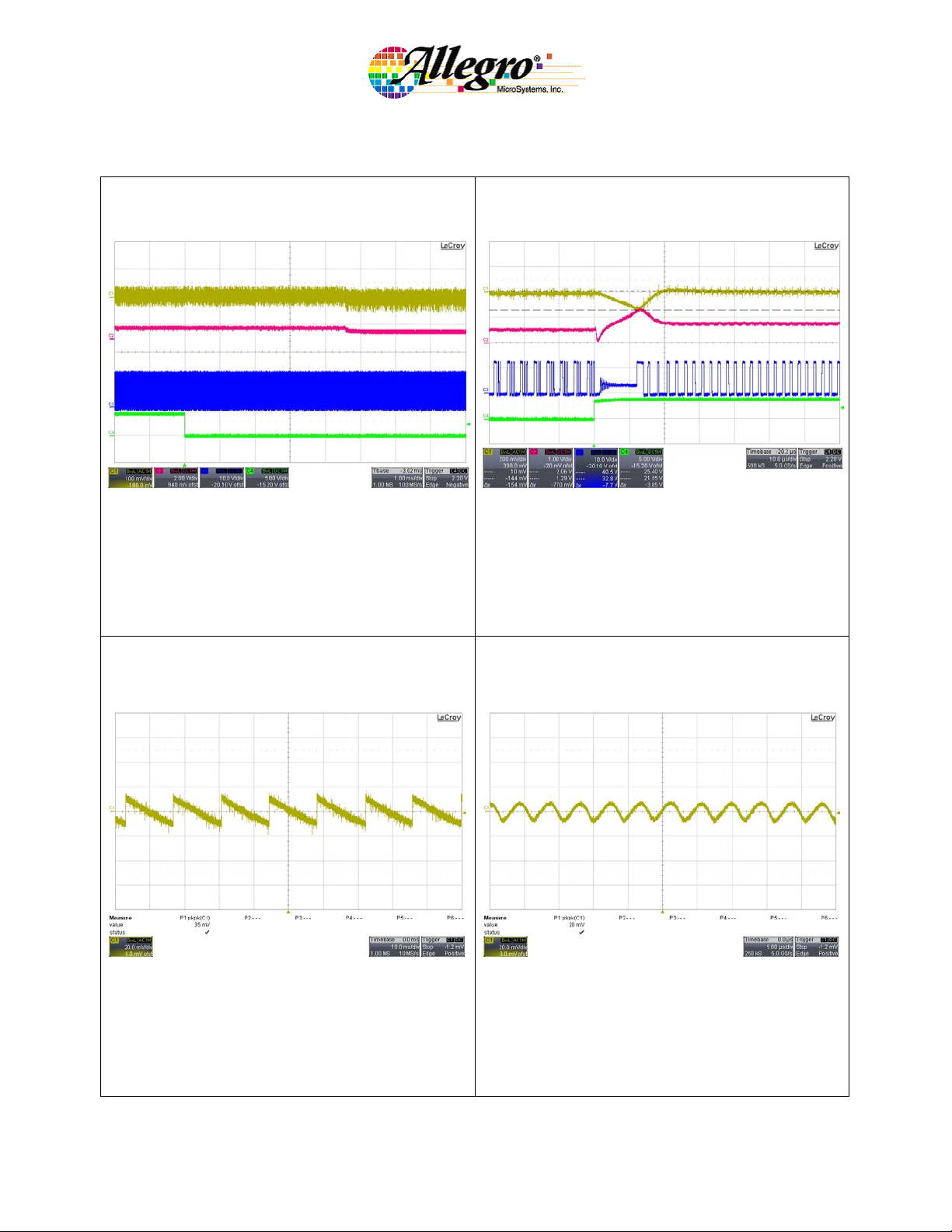
PWM to PFM Transition
12VIN, 470mA (7Ω) load
CH1=VOUT, CH2=COMP, CH3=SW,
CH4=PWM/PFMn
PFM to PWM Transition
12VIN, 470mA (7Ω) load
CH1=VOUT, CH2=COMP, CH3=SW,
CH4=PWM/PFMn
PFM Output Voltage Ripple
12VIN, 1mA (3.3KΩ) load
CH1=VOUT
PFM Output Voltage Ripple
12VIN, 400mA (8Ω) load
CH1=VOUT

Page 11 of 13 December 18th, 2012
DEMO BOARD PERFORMANCE
SW Voltage at 12VIN, 100mA load,
PWM/PFMn=1
CH3=SW
SW Voltage at 12VIN, 2.5A load,
PWM/PFMn=1
CH3=SW
Input Voltage Ripple at 12VIN, 2.5A load,
PWM/PFMn=1
CH1=VIN
Output Shorted, Hiccup Mode Operation,
PWM/PFMn=1
CH1=VOUT, CH2=COMP, CH3=SS, CH4=IL
Page 12 of 13 December 18th, 2012
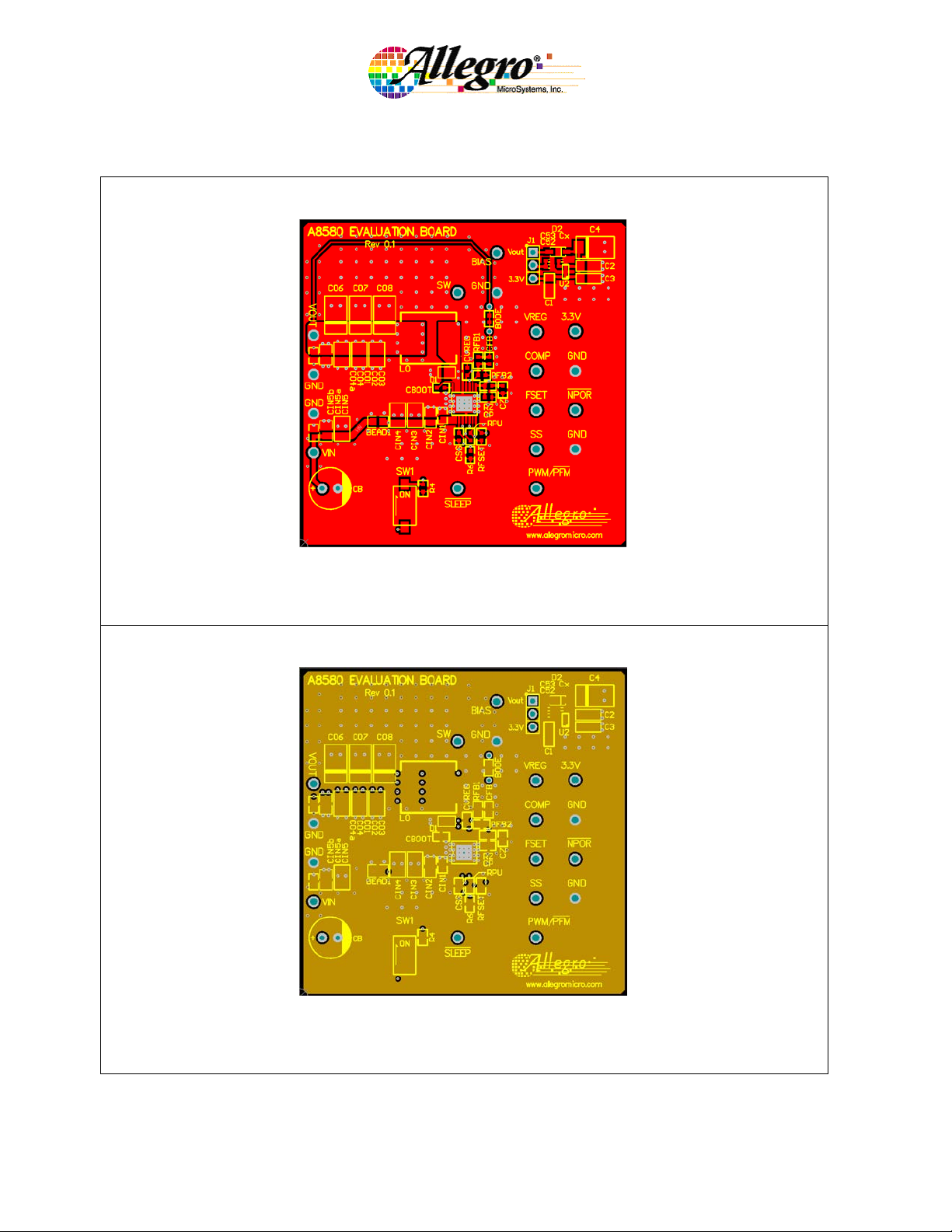
DEMO PCB LAYOUT
Top Layer and Top Silk
Layer 2 and Top Silk
Page 13 of 13 December 18th, 2012
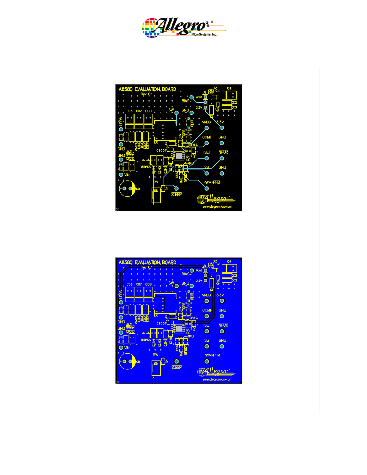
DEMO PCB LAYOUT
Layer 3 and Top Silk
Bottom Layer and Bottom Silk
Table of contents
Other Allegro Motherboard manuals


