Allegro A80803 User manual

User Manual
A80803 Evaluation Board and Programming GUI
UM-A80803, Rev. 1
MCO-0001115
February 4, 2022
INTRODUCTION
The A80803 Evaluation Board (EVB) is designed to aid sys-
tem designers with the evaluation of the operation and per-
formance of the A80803, a multi-topology, fixed frequency,
switch-mode DC/DC controller for LED lighting applica-
tions with built-in support for low/high-beam operation and
remote configuration via SPI.
The A80803 EVB is available in four configurations to sup-
port low/high-beam and fixed LED string applications. The
EVB arrives configured to operate in one of four modes and
has a mark on one of the silkscreen boxes in the top right of
the EVB to identify in which mode the EVB is configured.
The Allegro A80803 configuration GUI is a tool provided to
simplify interaction with the device using the SPI interface.
The tool can read and write all configuration registers as
well as report and clear the fault status and diagnostic bits.
The tool provides a tabbed interface to group similar options
together to help the user quickly find configuration options.
The GUI is not required for operation but simplifies con-
figuration register modifications.
Table 1: A80803 EVB Available Configurations
Configuration Name Part Number Low/High-Beam
Support
Low-Beam
Topology
High-Beam
Topology
Low/High Beam Topology Switch APEK80803KET-TS Yes Buck-Boost Boost
Low/High Beam Single FET APEK80803KET-SF Yes Boost Boost
Boost Only APEK80803KET-BO No Boost –
Buck-Boost Only APEK80803KET-BB No Buck-Boost –
Figure 1: A80803 EVB
Table of Contents
Introduction ...................................................................................1
General Setup...............................................................................2
Power Input ...............................................................................2
LED Connection ........................................................................2
Control Pins...............................................................................2
Bin Select ..................................................................................3
SPI Communication...................................................................3
Fault Flags.................................................................................3
Sense Resistor ..........................................................................4
Switching Frequency .................................................................4
NTC LED Current Derating .......................................................4
Getting Started with the GUI ......................................................... 5
GUI Troubleshooting .................................................................7
Device Configuration .................................................................8
Configuration Files and Default EEPROM ............................9
Diagnostics Tab ...................................................................10
Configuration Tab ................................................................ 11
Binning Tab.......................................................................... 11
Thermal Foldback Tab.........................................................12
VIN Foldback Tab ................................................................12
PWM Dimming Tab..............................................................13
High/Low-Beam Tab ............................................................14
Faults Flags Tab ..................................................................15
Writing to EEPROM.................................................................16
Low/High-Beam Topology Switch EVB .......................................17
APEK80803KET-TS Schematic ..............................................18
APEK80803KET-TS Bill of Materials.......................................19
Low/High-Beam Single FET EVB ...............................................20
Confirm HBGCTRL Bit.............................................................21
APEK80803KET-SF Schematic ..............................................22
APEK80803KET-SF Bill of Materials.......................................23
Boost Only EVB ..........................................................................24
APEK80803KET-BO Schematic..............................................25
APEK80803KET-BO Bill of Materials ......................................26
Buck-Boost Only EVB .................................................................27
APEK80803KET-BB Schematic ..............................................28
APEK80803KET-BB Bill of Materials....................................... 29
Board Layout...............................................................................30
Revision History ..........................................................................32

2
Allegro MicroSystems
955 Perimeter Road
Manchester, NH 03103-3353 U.S.A.
www.allegromicro.com
GENERAL SETUP
This section provides an overview of the connections that are generally applicable to all EVB configurations. Each group of connec-
tions is highlighted in Figure 2.
Figure 2: A80803 EVB I/O Connections
Power Input
Connect a power supply using the either X1 terminal block or the VBAT and GND test points.
LED Connection
Connect the anode of the LED string to the X2 connector terminal A (anode) and the cathode of the LED string to the X2 connec-
tor terminal K (cathode). For low/high-beam applications, tie the CT terminal to the LED string to mark the bottom of the low-beam
string. The APEK80803KET-BB and APEK80803KET-BO options have R18 and R23 installed to tie CT to the K terminal.
Control Pins
The LBEAMn, EN/PWM, and DIMn pins of the A80803 can be tied to VIN with jumpers or left open and controlled with external
signals. These test points could be tied to VIN externally or driven from a logic level source such as a microcontroller.
The jumpers J1, J2, and J3 can be installed or opened to set the operating state as shown in Table 2 and Table 3. To operate in external
dimming mode, install J2 or tie DIMn to a logic high signal and EN/PWM to an external PWM source for controlled dimming or logic
high for 100% dimming. To use internal dimming, open J2 and connect EN/PWM to logic high or install J3 and use the A80803 GUI
tool to set the LED brightness.
Table 2: Low/High-Beam Jumper
J1 (LBEAMn) State
Open Low-Beam
Installed High-Beam

3
Allegro MicroSystems
955 Perimeter Road
Manchester, NH 03103-3353 U.S.A.
www.allegromicro.com
Table 3: Internal/External Dimming Jumpers
J2 (DIMn) J3 (EN/PWM) Dimming Mode
Installed Installed External - 100%
Installed Open External - PWM
Open Installed Internal
Bin Select
Jumpers J4 to J7 select the bin for analog dimming.
Note: Only one bin select jumper should be installed at a time. See Table 4 for bin selection.
Table 4: BIN Selection Jumpers
Jumper Installed BIN
J4 BIN1 selected
J5 BIN2 selected
J6 BIN3 selected
J7 BIN4 selected
Gain can be modified for each bin using the A80803 GUI tool; see the Binning Tab section of this document. The jumpers J4 to J7
select a resistor for the bottom of a voltage divider. If all four jumpers are open, the BINSEL pin will be pulled up to VCC and BIN1
will be selected.
SPI Communication
The A80803 supports SPI for serial communication to control the configuration registers. The silkscreen labels are intended for use
with the FTDI USB to Serial adapter cable, part number C232HM-EDHSL-0, to be used with the A80803 GUI tool. See Table 5 to
compare the silkscreen labels to the SPI pin names. The jumpers J1, J2, and J3 can be installed or opened to set the operating state as
shown in Table 2 and Table 3. To operate in external dimming mode, install J2 or tie DIMn to a logic high signal and EN/PWM to an
external PWM source for controlled dimming or logic high for 100% dimming. To use internal dimming, open J2 and connect EN/
PWM to logic high or install J3 and use the A80803 GUI tool to set the LED brightness.
Table 5: J8 Header SPI Labels
Silkscreen Label USB-Serial Breakout Wire SPI Pin
ORN Orange SCK
YEL Yellow MOSI
GRN Green MISO
BRN Brown CSn
BLK Black GND
Fault Flags
There are two active low fault flag pins on the A80803, FFn1 and FFn2. Both are available as test points on the EVB. The fault flags
are pulled up to VCC with a 10 kΩ resistor on the EVB.

4
Allegro MicroSystems
955 Perimeter Road
Manchester, NH 03103-3353 U.S.A.
www.allegromicro.com
Sense Resistor
The LED current is set by the sense resistor R2 and the equation:
ILED = VIDL / R2
Each EVB configuration is designed for a 1 A LED current; with VIDL = 200 mV then R2 = 0.2 Ω.
Switching Frequency
The switching frequency for the power converter stage is set by R16 and the equation:
fSW = 35000 / R16
where fSW is in kHz and R16 is in kΩ. Each EVB configuration is designed for a switching frequency of 400 kHz with R16 = 86.6 kΩ.
NTC LED Current Derating
There is a NTC thermistor on the EVB, RT1, in a voltage divider leading to the NTC pin. The thermistor, part number NTCS0603E-
3103FHT, has a base resistance of 10 kΩ. See the Thermal Derating section in the A80803 datasheet for more information about
programming the derating values.

5
Allegro MicroSystems
955 Perimeter Road
Manchester, NH 03103-3353 U.S.A.
www.allegromicro.com
GETTING STARTED WITH THE GUI
Download the A80803 GUI tool from https://registration.allegromicro.com. The GUI tool is an executable that can be run directly
without any additional installation steps once downloaded and extracted. The tool depends on the FTDI D2xx driver for USB to Serial
communication.
Note: Text highlighted in blue monospaced font refers to a button in the GUI.
The tool opens to the Diagnostic tab but does not attempt to communicate with the part until the user requests a read or write opera-
tion. The initial state of the GUI is shown below in Figure 3.
Figure 3: First screen after starting the GUI
Figure 4: USB Serial Connection Established
Press the Read Faults button to start a read and initialize the USB connection. Upon successful connection, the USB status will
change to USB Connected in green text in the bottom left corner of the window.

6
Allegro MicroSystems
955 Perimeter Road
Manchester, NH 03103-3353 U.S.A.
www.allegromicro.com
At the top of the diagnostics tab there are buttons to read all configuration data from shadow or EEPROM into the state of GUI
controls, and to write the full state of the GUI controls to the configuration registers or EEPROM. A good practice is read the shadow
registers, once the connection to the A80803 has been established, by clicking the Read Shadow button shown in Figure 5, to align the
GUI controls with the state of the device. Reading the full contents of the EEPROM can be used to understand what is programmed
into EEPROM and is loaded into shadow at each power-on, but the shadow registers are what the A80803 uses during operation.
Figure 5: Read All of Shadow to Align GUI Controls with the Device

7
Allegro MicroSystems
955 Perimeter Road
Manchester, NH 03103-3353 U.S.A.
www.allegromicro.com
If this error appears and the D2xx drivers are believed to be installed, then ensure the USB cable is fully connected to the PC. If the
USB cable was recently plugged-in, then ensure the PC has had enough time to recognize the USB device.
If the GUI shows USB Connected and Parity check failed as shown in Figure 7, this means the USB-to-serial converter is con-
nected but cannot communicate to the A80803. Ensure the A80803 SPI pins are properly connected in the correct order (refer to the
SPI Communication section of this document), and the device is powered. A parity error while reading the fault registers will reset the
fault indicators to black text to indicate the state is unknown.
Figure 7: GUI is connected to USB-Serial but cannot nd A80803
The window on the right side of the GUI window shows the details of each SPI transaction as they are processed. The bottom of the
window shows the diagnostic information from on the MISO pin after each SPI read or write. See the Serial Communication section in
the datasheet for more details about the SPI interface.
GUI Troubleshooting
After the first read or write request, the tool will attempt to communicate using the FTDI D2xx driver. If the driver is not installed, or
the FTDI USB-Serial device cannot be found, an error message will be displayed as shown in Figure 6.
Figure 6: Error when FTDI device cannot be found
8
Allegro MicroSystems
955 Perimeter Road
Manchester, NH 03103-3353 U.S.A.
www.allegromicro.com
Device Configuration
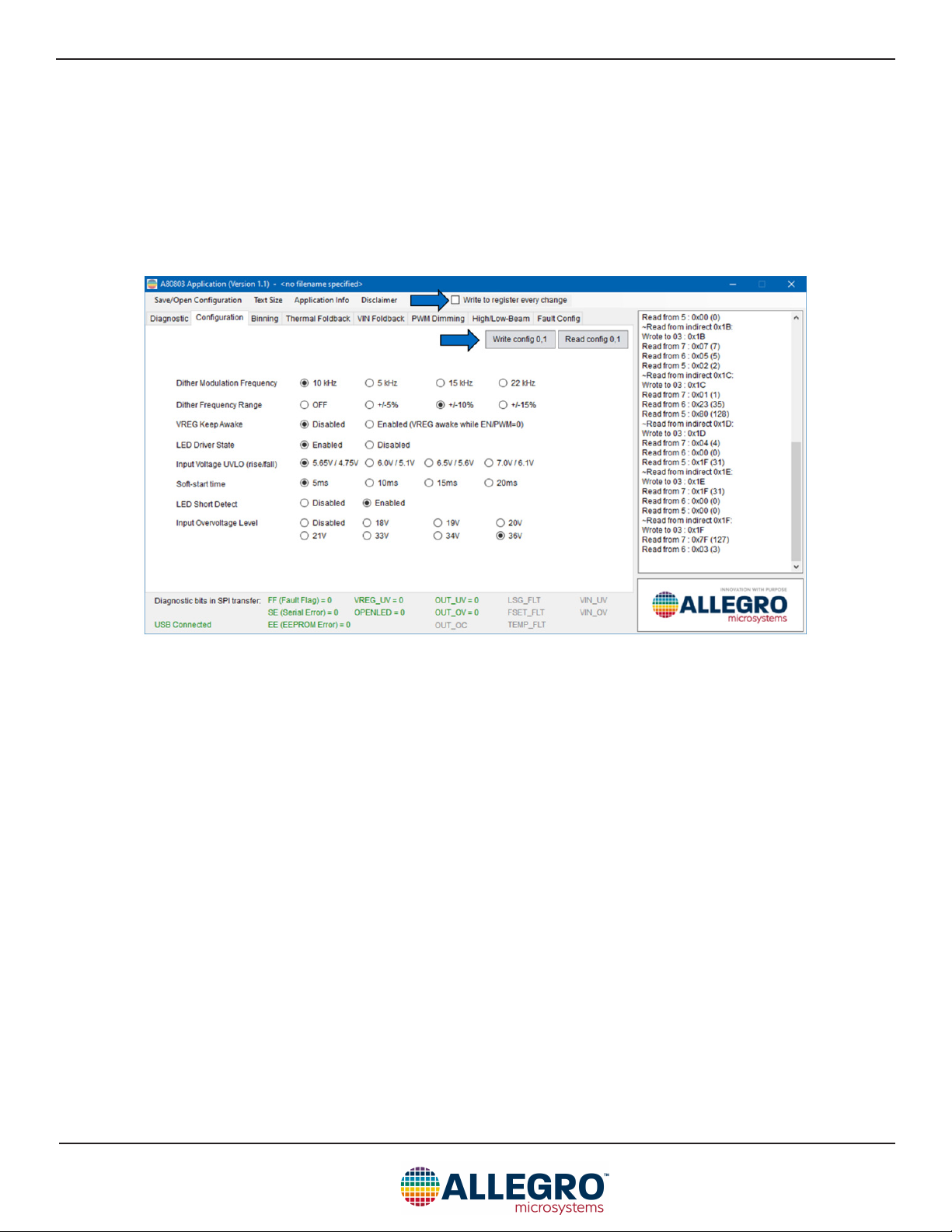
Each of the other tabs after the Diagnostics tab has two buttons in the top right corner, one to read just the registers represented on
that tab, Read config, and one to write the state of the GUI controls in that tab to those registers, Write config. The numbers in
the button label indicate the Config registers affected. There is also a checkbox near the top of the window for Write to register
every change which will update configuration registers every time a change is made without having to make the change and click
the Write button.
Figure 8: Read, Write, and Write Every Change

9
Allegro MicroSystems
955 Perimeter Road
Manchester, NH 03103-3353 U.S.A.
www.allegromicro.com
Configuration Files and Default EEPROM
The GUI tool has an option to save its state to a file to be recalled later. Click on the Save/Open Configuration menu item, then
click Save this configuration to afile..., and select a location and name the file, shown in Figure 9. Recall this configura-
tion by clicking the Save/Open Configuration button, select Open device configuration file..., and select the file to
load. After loading a configuration file, the GUI will update to match the state when it was saved.
At any time, the factory default EEPROM state can be loaded into the GUI controls by selecting Load default configuration to
application option from the Save/Open menu.
Note: Loading a configuration (including the default) does not automatically send the configuration to the device, giving an oppor-
tunity to modify a loaded configuration before writing to the device.
Figure 9: Save and Load Conguration Files

10
Allegro MicroSystems
955 Perimeter Road
Manchester, NH 03103-3353 U.S.A.
www.allegromicro.com
Diagnostic Tab
In addition to the buttons to read or write the full register set, the Diagnostic tab also shows the status of the faults captured in the
DIAG0 and DIAG1 registers. The fault status indicators will update with each click of the Read Faults button or continuously if the
Continuous Fault Read button is pressed. The fault status indicators will be green and show a value of 0 when no fault is present
and red with a value of 1 when a fault is present. Some faults are latched and must be cleared with the Clear Faults button. See
DIAG0 and DIAG1 register descriptions in the datasheet for more information.
Figure 10: Fault Indicators
The bottom of the GUI window shows the faults that are on the MISO line during every SPI transaction. The faults in gray in Fig-
ure 10 are only available on the MISO line during a write. See the SPI Data Frames section of the datasheet for more information.

11
Allegro MicroSystems
955 Perimeter Road
Manchester, NH 03103-3353 U.S.A.
www.allegromicro.com
Configuration Tab
The Configuration tab provides several general purpose options to configure the A80803, as shown in Figure 11.
Figure 11: General Conguration
Binning Tab
The Binning tab has four sliders to control the bin gain for each of the four bins. The binning level acts as a derating for the maximum
LED current. The BINSEL pin (a resistor divider from VCC selectable by jumpers on the evaluation board) selects which bin is active;
see the Bin Select section of this document and the LED Analog Dimming section of the datasheet for more information about binning
with the A80803.
Figure 12: Binning Conguration
12
Allegro MicroSystems
955 Perimeter Road
Manchester, NH 03103-3353 U.S.A.
www.allegromicro.com
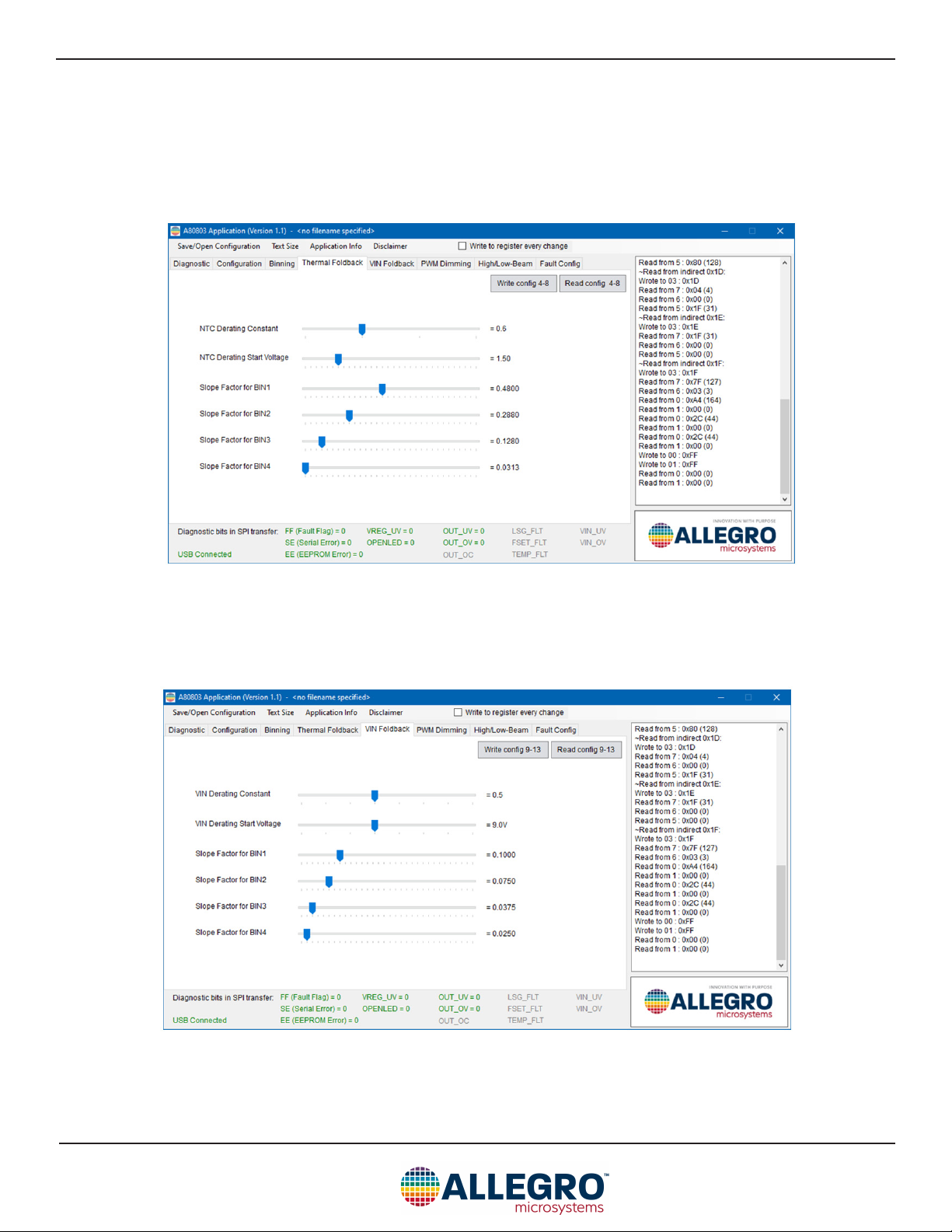
Thermal Foldback Tab
The Thermal Foldback tab has sliders for the NTC analog dimming options. See the Thermal Derating section and the Thermal Derat-
ing Example in the datasheet for more information about calculating these values.
Figure 13: Thermal Foldback Conguration
VIN Foldback Tab
The VIN Foldback tab has sliders for the VIN derating analog dimming options. See the Input Voltage Derating section and the Input
Voltage Derating Example in the datasheet for more information about calculating these values.
Figure 14: Input Voltage Foldback Conguration

13
Allegro MicroSystems
955 Perimeter Road
Manchester, NH 03103-3353 U.S.A.
www.allegromicro.com
PWM Dimming Tab
This tab has options related to PWM dimming and includes the following options for internal PWM dimming: a toggle selection for
Internal PWM Dimming Override, four options for Internal PWM Dimming Frequency, and a slider for Internal PWM Dim-
ming Duty Cycle. The Internal/External PMOSFET Gate Current option applies to the PWMOUT gate driver for both inter-
nal and external PWM dimming. See the LED PWM Dimming section of the datasheet for more information about PWM dimming
with the A80803.
Note: If the DIMn pin is low, the Internal PWM Dimming Duty Cycle slider will set the PWM dimming duty cycle even if
Internal PWM Dimming Override is set to Disabled because the device will honor the DIMn selection for internal PWM.
Figure 15: PWM Dimming Conguration

14
Allegro MicroSystems
955 Perimeter Road
Manchester, NH 03103-3353 U.S.A.
www.allegromicro.com
High/Low-Beam Tab
The High/Low-Beam tab has options to set the overvoltage and undervoltage thresholds for both low-beam and high-beam, the
overvoltage behavior, the additional dead time setting, and high-beam gate controls. The high-beam gate can be forced on with the
High-beam Gate On/Off option, and the HBG Control option can be set to invert how HBG reacts to the LBEAMn pin (this
option should only be used with the application circuit for low/high-beam transitions that short out the high-beam LEDs; see APE-
K80803KET-SF for an evaluation board of this application. Also see Low and High Beam Control section of the datasheet for more
information.
Note: Allegro recommends setting low-beam and high-beam overvoltage limits approximately 5 V above the expected output voltage.
Figure 16: PWM Dimming Conguration

15
Allegro MicroSystems
955 Perimeter Road
Manchester, NH 03103-3353 U.S.A.
www.allegromicro.com
Figure 17: Fault Flag Conguration
Fault Flags Tab
The Fault Flags tab has options to set which faults are reported on FFn2, the FFn2 delay, the overcurrent detection filter, and the one-
out-all-out behavior.

16
Allegro MicroSystems
955 Perimeter Road
Manchester, NH 03103-3353 U.S.A.
www.allegromicro.com
Writing to EEPROM
The EEPROM must be unlocked before it can be written. Unlocking the EEPROM must be the first SPI transaction after the device is
powered. To unlock and write EEPROM with the GUI, follow this procedure:
1. Power on the device and read the faults to verify communication.
2. Power cycle the A80803 while keeping the GUI open.
3. Click the Unlock EEPROM button (this must be rst button after A80803 is powered).
4. If the unlock was successful, the text above the unlock button will read EEPROM Writes Unlocked in green text.
5. Click the Read Shadow button to read the full shadow register contents into the GUI.
Note: If this step is skipped, the full state of the GUI will still be written into the full EEPROM in Step 7. Reading shadow
before making changes to the GUI is the best practice to ensure only the desired settings are modified in EEPROM.
6. Update the controls on any tab to the desired state to be written into EEPROM.
7. Return to the Diagnostic tab and click the Write EEPROM button to write all conguration data to EEPROM.
8. Optionally, power-cycle and use the Read Shadow button to verify the shadow registers are updated with the new values on
power-up.
Figure 18: EEPROM Writes Unlocked
Note: If needed, to restore the EEPROM to the factory settings, load the default configuration into the GUI (see Configuration Files)
and write it to EEPROM.

17
Allegro MicroSystems
955 Perimeter Road
Manchester, NH 03103-3353 U.S.A.
www.allegromicro.com
LOW/HIGH-BEAM TOPOLOGY SWITCH EVB
The low/high-beam topology switch configuration operates in buck-boost mode while in low-beam and in boost mode while in high-
beam. This allows for shorter low-beam strings that may have an output voltage less than the input voltage. Connect the LED string to
terminal block X2 as shown in Figure 19, where terminal A to CT is the low-beam string, and terminal A to K is the high-beam string.
Connect a power supply as described in the Power Input section of this document and set the jumpers to achieve the desired dimming
option as described in the Control Pins section. Connect the FTDI USB breakout cable to J8 for optional software configuration and
fault readback.
When LBEAMn is low, Q4 is on and Q5 is off, directing the LED current from the LED anode through the CT terminal and through
Q4 back to VIN. When LBEAMn is high, Q4 is off and Q5 is on, directing the LED current through the full LED string and through
Q5 to ground.
Figure 19: APEK80803KET-TS PCB with LED Connection

18
Allegro MicroSystems
955 Perimeter Road
Manchester, NH 03103-3353 U.S.A.
www.allegromicro.com
APEK80803KET-TS SCHEMATIC
Figure 20: APEK80803KET-TS Schematic

19
Allegro MicroSystems
955 Perimeter Road
Manchester, NH 03103-3353 U.S.A.
www.allegromicro.com
APEK80803KET-TS Bill of Materials
Designator Description Quantity Manufacturer Manufacturer P/N
U1 A80803 in the QFN-32 1 Allegro MicroSystems
C1 Capacitor, Ceramic, 0.1 µF, 50 V, X7R, 0603 1
C2, C3, C4 Capacitor, Ceramic, 4.7 µF, 50 V, X7R, 1210 3 Murata GCM32ER71H475KA55K
C5, C9 Capacitor, Ceramic, 0.1 µF, 50 V, X7R, 0805 2
C6, C7, C8 Capacitor, Ceramic, 4.7 µF, 100 V, X7R, 1210 3 TDK CNA6P1X7R2A475K250AE
C10 Capacitor, Ceramic, 47 nF, 25 V, X7R, 0402 1
C11 Capacitor, Ceramic, 0.1 µF, 16 V, X7R, 0402 1
C12 Capacitor, Ceramic, 4.7 µF, 16 V, X7R, 0805 1
C13, C14 Capacitor, Ceramic, 2.2 µF, 16 V, X7R, 0805 2
C15, C19 Capacitor, Ceramic, 4.7 nF, 50 V, X7R, 0402 2
C16 Capacitor, Ceramic, 33 pF, 50 V, C0G, 0603 1
C17 Capacitor, Ceramic, 820 nF, 25 V, X7R, 0603 1
C18 Capacitor, Ceramic, 47 nF, 50 V, X7R, 0603 1
D1 Diode, Schottky, 60 V, 5 A, SOD-128 1 Nexperia PMEG60T50ELPX
D4 Diode, Schottky, 100 V, 2 A, SOD123W 1
GND1, GND2 Ground Bar, 18 AWG Bus Bar, 15 mm Body 2
J1, J2, J3, J4, J5, J6, J7 Connector, Header, 2 Position, 0.1" 7 Wurth 61300211121
J8 Connector, Header, 5 Position, 0.1" 1 Wurth 61300511121
L1 Inductor, 33 µH, ±20%, 8 A sat, 85.5 mΩ Max 1 Eaton HCMA1305-330-R
Q1, Q3 MOSFET, N-Channel, 30 A, 100 V, LFPAK56 2 Nexperia PSMN038-100YL
Q2, Q4 MOSFET, P-Channel, 100 V, 15 A, TO252-3 2 Infineon SPD15P10PLGBTMA1
Q5 MOSFET, N-Channel, 14.8 A, 100 V, LFPAK56 1 Nexperia BUK9Y104-100B
R1 Resistor, 100 kΩ, 1/16W, 1%, 0402 1
R2 Resistor, 0.2 Ω, 1 W, 1%, 2512 1
R3 Resistor, 150 Ω, 1/16 W, 1%, 0402 1
R4, R5, R11, R12, R13, R20 Resistor, 10 kΩ, 1/16 W, 1%, 0402 6
R6, R10 Resistor, 0 Ω, 1/16 W, 1%, 0402 2
R7, R23 Resistor, 0 Ω, 1/10 W, 0603 2
R9, R26 Resistor, 2.4 kΩ, 1/16 W, 1%, 0402 2
R14 Resistor, 2.21 kΩ, 1/16 W, 1%, 0402 1
R15 Resistor, 1.54 kΩ, 1/16 W, 1%, 0402 1
R16 Resistor, 86.6 kΩ, 1/16 W, 1%, 0402 1
R17 Resistor, 45.3 Ω, 1/10 W, 1%, 0603 1
R19 Resistor, 24.9 kΩ, 1/16 W, 1%, 0402 1
R21 Resistor, 5.1 kΩ, 1/16 W, 1%, 0402 1
R22 Resistor, 1 kΩ, 1/16 W, 1%, 0402 1
R24, R25 Resistor, 0.12 Ω, 1 W, 1%, 2512 2
R28 Resistor, 5.36 kΩ, 1/16 W, 1%, 0402 1
RT1 Thermistor, NTC, 10 kΩ, 0603 1 Vishay NTCS0603E3103FHT
TP1, TP2, TP4, TP5, TP6, TP7,
TP8, TP9, TP10, TP11 Test Point, Red, 0.063" Diameter 10 Keystone 5010
TP3 Test Point, Black, 0.063" Diameter 1 Keystone 5011
X1 Terminal Block, 5.08 mm, Vertical, 2 position 1 TE Connectivity 282837-2
X2 Terminal Block, 5.08 mm, Vertical, 4 position 1 TE Connectivity 282837-4

20
Allegro MicroSystems
955 Perimeter Road
Manchester, NH 03103-3353 U.S.A.
www.allegromicro.com
LOW/HIGH-BEAM SINGLE FET EVB
The low/high-beam single FET configuration operates in boost mode for both low-beam and high-beam and shorts out the high-beam
part of the LED string while in low-beam. The LED string must have enough LEDs for the boost output voltage to be higher than the
input voltage for both low-beam and high-beam. Connect the LED string to terminal block X2 as shown in Figure 21, where A to CT
is low-beam, and A to K is high-beam. Connect a power supply as described in the Power Input section of this document and set the
jumpers to achieve the desired dimming option as described in the Control Pins section. Connect the FTDI USB breakout cable to J8
for optional software configuration and fault readback.
When LBEAMn is low, the high-beam LEDs are shorted to ground by Q5, and when LBEAMn is high, Q5 is open and the LED cur-
rent flows through the high-beam LEDs and returns through the cathode terminal to ground.
Figure 21: APEK80803KET-SF PCB with LED Connection
Note: This EVB requires EEPROM bit HBGCTRL = 1, which is different from the other EVBs and the default EEPROM which sets
HBGCTRL = 0. See the Confirm HBGCTRL Bit section before powering up LEDs.
This manual suits for next models
4
Table of contents
Other Allegro Motherboard manuals


Popular Motherboard manuals by other brands


InvenSense
InvenSense AN-000013 user guide

YIC Technologies
YIC Technologies EVK-YIC51612EBGG-33 user guide

Global American Inc.
Global American Inc. 2801020 user manual

Global American Inc.
Global American Inc. 3302140 manual

HIK VISION
HIK VISION DS-5116HFI Series user manual

USOUND
USOUND TARVOS 1.0 UC-E3010 user manual