EVAL-AD4114SDZ User Guide UG-1819
Rev. 0 | Page 5 of 24
EVALUATION BOARD HARDWARE
DEVICE DESCRIPTION
The AD4114 is a highly accurate, high resolution, multiplexed,
Σ-Δ ADC with 16 single-ended or 8 differential voltage inputs,
and a voltage range of −10 V to +10 V. The maximum channel
to channel scan rate is 6.21 kSPS (161 μs) for fully settled data.
The output data rates range from 1.25 SPS to 31.25 kSPS. The
device includes integrated analog reference buffers, an integrated
precision 2.5 V reference, and an integrated oscillator.
See the AD4114 data sheet for complete specifications. Consult
the data sheet in conjunction with this user guide when using
the evaluation board.
HARDWARE LINK OPTIONS
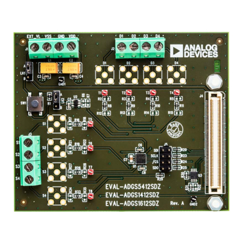
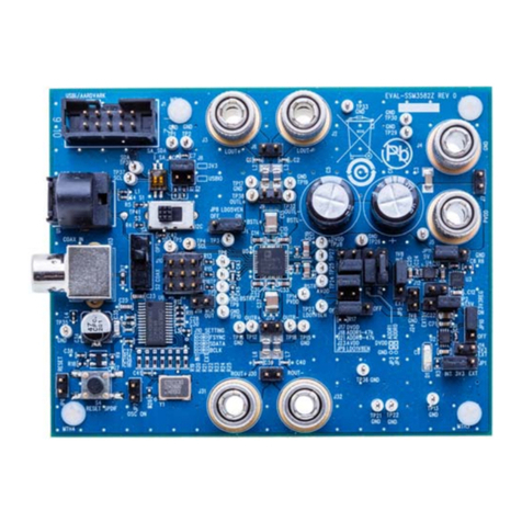
See Table 1 for the default link options. By default, the EVAL-
AD4114SDZ is powered from and controlled by the SDP board
connected to J12. The ADuM5411 (U3) output is set to 5 V.
EVALUATION BOARD SETUP PROCEDURE
After following the instructions in the Software Installation
Procedures section, set up the EVAL-AD4114SDZ and SDP
board as detailed in the Configuring the EVAL-AD4114SDZ and
SDP Boards section.
The evaluation software and drivers must be installed before
connecting the EVAL-AD4114SDZ and SDP board to the USB
port of the PC to ensure that the PC correctly recognizes the
evaluation system.
Configuring the EVAL-AD4114SDZ and SDP Boards
Use the following procedure to configure the boards:
1. Connect the SDP board to Connector A or Connector B on
the EVAL-AD4114SDZ. Screw the two boards firmly
together using the plastic screw and washer set included in
the evaluation board kit.
2. If using the SDP-K1 board, the Arduino headers can also be
used to connect to the EVAL-AD4114SDZ. If the Arduino
headers are used, the J6 links must be changed to ARD.
3. Ensure that LK3 is in Position B (USB).
4. Connect the SDP board to the PC using the USB cable.
Table 1. Default Link and Solder Link Options
Link Default Option Description
LK1 Inserted Connects the on-board external reference ADR4525ARZ (U2) to AD4114 (U1). Remove LK1 if using a
different single-ended external reference.
LK2 Inserted Connects VINCOM to GND_ISO. This configuration is typical for single-ended measurement. Remove LK2 to
set the custom common analog input for single-ended channels. VINCOM is available on Pin 5 of J3.
LK3 B (USB) Selects the power supply voltage.
Position A: EVAL-AD4114SDZ is powered from the external dc power supply connector, J4.
Position B: EVAL-AD4114SDZ is powered from the USB through the SDP or Arduino connector.
LK4 to LK6 SDP Selects which Arduino serial peripheral interface (SPI) lines to connect to J6.
STD: Standard Arduino headers.
ALT: Alternate in-circuit serial programming (ICSP) header.
LK7, LK8 SDP Selects the I2C source for the on board electronically erasable programmable read-only memory (EEPROM).
SDP: SDP connector.
ARD: Arduino header.
LK9, LK10 Inserted Connects VIN4 and VIN5 to the Zener diodes, D16 and D17, respectively. VIN4 and VIN5 can be removed to
evaluate the voltage inputs of the AD4114 directly by removing external components.
LK11, LK12 Removed Bypasses R10 and R11 on VIN4 and VIN5, respectively.
By inserting this link, the resistor is removed from the input path and AD4114 can be evaluated directly.
J6 SDP Selects between the Arduino headers and the SDP connector, and has the active connector for power and SPI
signals.
SDP: SDP connector.
ARD: Arduino header.
J14 CS0 Selects which GPIOx pin to use on the Arduino header to enable CS connections when stacking evaluation
boards.
R35 Open Sets the ADuM5411 (U3) isolated regulator output voltage.
Open: +VA_ISO = 5 V.
Short: +VA_ISO = 3.3 V.
