EVAL-AD5317RDBZ User Guide UG-970
Rev. A | Page 3 of 13
EVALUATION BOARD HARDWARE
MOTHERBOARD POWER SUPPLIES
The E VA L -MBnanoDAC-SDZ motherboard supports single
and dual power supplies.
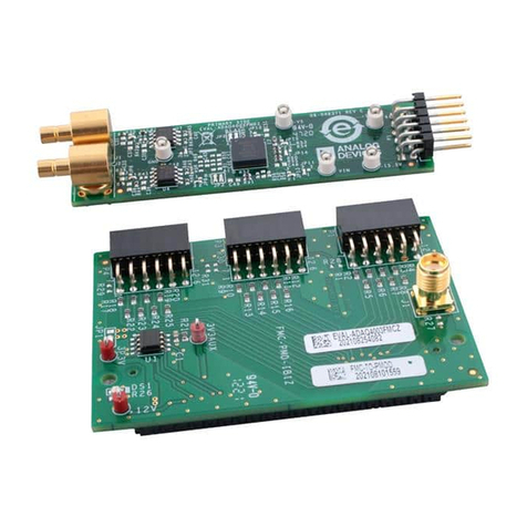
The E VA L -AD5317RDBZ evaluation board can be powered
either from the SDP port or externally using the J5 and J6
connectors, as described in Table 1.
Table 1. Power Supply Connectors
Connector No. Label Voltage
J5, Pin 1 (J5-1) VDD Analog positive power supply, VDD
single supply 5 V, dual supply 5 V.
J5, Pin 2 (J5-2) AGND Analog ground.
J5, Pin 3 (J5-3) VSS Analog negative power supply, VSS
dual supply −5 V.
J6, Pin 1 (J6-1) VLOGIC Digital supply from 1.8 V to VDD of
the daughter board DAC.
J6, Pin 2 (J6-2) DGND Digital ground.
Both the AGND and DGND inputs are provided on the board.
The AGND and DGND planes are connected at one location on
the E VA L-MBnanoDAC-SDZ. It is recommended that AGND
and DGND not be connected elsewhere in the system to avoid
ground loop problems.
All supplies are decoupled to ground with 10 µF tantalum and
0.1 µF ceramic capacitors.
MOTHERBOARD LINK OPTIONS
A number of link options are incorporated in the EVA L -
MBnanoDAC-SDZ and must be set for the required operating
conditions before using the board. Table 2 describes the positions
of the links to control the evaluation board via the SDP-B board
using a PC and external power supplies. The functions of these
link options are described in detail in Table 3. The positions listed
in Table 2 and Table 3 match the evaluation board imprints (see
Figure 12).
Table 2. Link Options Setup for SDP-B Control (Default)
Link No. Position
REF1 2.5V
REF2 EXT
REF3 EXT
REF4 EXT
LK5 C
LK6 3.3V
LK7 B
DAUGHTER BOARD LINK OPTIONS
The printed circuit board (PCB) for this board is shared between
the E VA L-AD5316RDBZ and E VA L -AD5317RDBZ daughter
boards. To configure for the E VA L-AD5317RDBZ daughter
board, it is recommended that LK1 and LK2 be removed for
proper device operation.
Table 3. Link Functions
Link No. Function
REF1 to REF4 These links select the reference source.
Position EXT selects an off-board voltage reference via the appropriate EXT_REF_x connector.
Position VDD selects VDD as the reference source.
Position 4.096V selects the on-board 4.096 V reference as the reference source.
Position 2.5V selects the on-board 2.5 V reference as the reference source.
Position 5V selects the on-board 5 V reference as the reference source.
LK5 This link selects the positive DAC analog voltage source.
Position A selects the internal voltage source from the SDP-B board. Only the 2.5 V on-board reference can be used
with this configuration.
Position B selects the internal voltage source 3.3 V from the ADP121 on the motherboard.
Position C selects an external supply voltage, VDD.
LK6 This link selects the VLOGIC voltage source.
Position 3.3V selects the digital voltage source from the SDP-B board, 3.3 V.
Position VLOGIC selects an external digital supply voltage, VLOGIC.
LK7 This link selects the negative DAC analog voltage source.
Position A selects VSS.
Position B selects AGND.
