www.analog.com Analog Devices
│
5
MAX14916PMB Evaluates: MAX14916
Pmod Style Connector
The MAX14916PMB# can plug directly into a Pmod-
compatible port through J1. Note the pin definitions are
determined by the USB2PMB2# or USB2GPIO# adapter,
and to use this board with own host, configure the micro-
controller or FPGA to match the MAX14916PMB# J1 pin-
out. For more information on the MAX14916 SPI interface
and control, refer to the MAX14916 IC data sheet. See the
MAX14916PMB schematic for the J1 pinout.
Power Supply
A 24V DC power adapter, SDI65-24-UDC-P5, with a
maximum of 2.71A output current is included with the
MAX14916PMB# and must be connected to J2 for normal
operation. For a higher total load current on the output
than the power adapter can provide, use own DC power
supply. Note the MAX14916 is specified for operation with
a supply voltage up to 36V and is tolerant to 65V. The
barrel connector J2 is rated up to 5A maximum. Do not
operate beyond these maximum ratings.
Light-Emitting Diodes (LEDs)
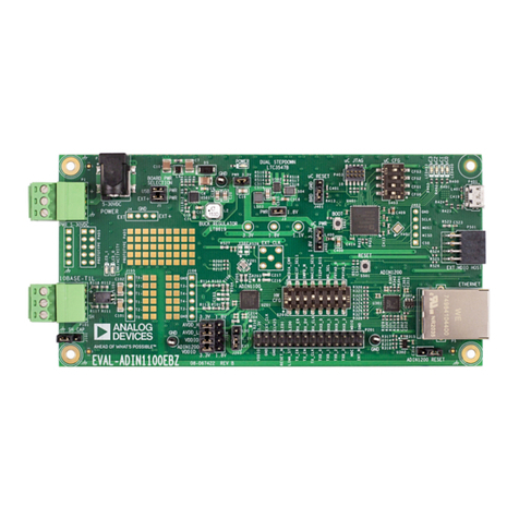
The MAX14916PMB# comes with a 4 x 2 LED matrix,
providing four green LEDs indicating per-channel input or
output status, and four red LEDs indicating per channel
fault conditions. See Table 1 for a full list of each chan-
nel’s corresponding status and fault LEDs. If a fault LED
is turned on for a channel, the corresponding status LED
is always turned off. This mitigates false information about
the status of the affected channel.
Field supply (VDD) diagnostic faults are provided through
the VDDOK LED (DS9 - green). The Munich GUI pro-
vides limited access to the diagnostic features of the
MAX14916. To explore the full diagnostic capabilities of
the MAX14916, refer to the MAX14916 evaluation kit.
Transient Immunity Protection
No external surge suppression is needed on OUT_ pins
as they are protected against ±1kV surge pulses per IEC
61000-4-5. Connect a TVS diode between VDD and GND
to clamp positive surge pulses on the OUT_ and VDD
pins. The MAX14916PMB# outputs are protected against
±1kV surge transients with TVS diode D1, SMBJ36A, con-
nected between VDD and GND.
Addressable SPI
Figure 5. Digital Output Operation Mode Configuration
The MAX14916 supports addressable SPI, allowing direct
communication with up to four MAX14916 devices. By
default, the MAX14916PMB# is configured as address
00, with A1 = 0 and A0 = 0. It is possible to change the
SPI address using the provided resistor footprints by con-
necting A1 and A0 to VL or GND using the pads provided
at R10 and R11. Note that if the SPI address is changed
from the default value, it no longer works with the pro-
vided Munich GUI software and the user must develop
own software to support the new SPI address. For more
information on SPI device address selection, refer to the
MAX14916 IC data sheet.
Table 1. MAX14916PMB# LED Channel
Assignments
CHANNEL
NUMBER
STATUS LED
(GREEN)
FAULT LED
(RED)
1 DS2 DS6
2 DS4 DS8
3 DS1 DS5
4 DS3 DS7

