User Guide DC3251A
QUICK START PROCEDURE
analog.com Rev. 0 | 5 of 13
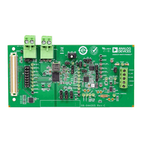
Demonstration circuit DC3251A is easy to set up and use to evalu-
ate the performance of the LTC3302A. For the proper measurement
equipment setup, see Figure 3 and follow the procedure below:
NOTE: For accurate VIN, VOUT, and efficiency measurements,
measure VIN at the VIN SNSE and GND SNSE turrets, and VOUT
at the VOUT SNSE and GND SNSE turrets as shown as VM1 and
VM2 in Figure 3. When measuring the input or output voltage ripple,
care must be taken to avoid a long ground lead on the oscilloscope
probe. Measure the output voltage ripple by touching the probe
tip directly across the output turrets or to TP1 as shown in Figure
4. TP1 is designed for a 50 Ω coax cable to reduce any high
frequency noise that might couple into the oscilloscope probes.
1. Set the JP1 Jumper to the SKIP position and JP2 to the HI
position.
2. With power off, connect the input power supply to VIN and GND.
If the input EMI filter is required, connect the input power supply
to VIN EMI.
3. Slowly increase PS1 to 1.0 V. If AM1 reads less than 20 mA,
increase PS1 to 3.3 V. Verify that VM1 reads 3.3 V and VM2
reads 1.2 V.
4. Connect an oscilloscope voltage probe as shown in Figure 4
in parallel with VM2. Set Channel to AC-coupled, voltage scale
to 20 mV and time base to 10 µs. Observe the VOUT ripple
voltage.
5. Verify that PGOOD turret is above 1 V.
6. Increasing the load by 1 A intervals up to 2 A and record VM1,
VM2, AM1, and AM2 for each interval.
7. Repeat step 6 for PS1 set to 2.5 V and again for PS1 set to 5.0
V.
8. Set the load to a constant 1 A. Remove the oscilloscope voltage
probe from VOUT. Place a ground clip on PGND terminal and
set the voltage scale to 1 V and the time scale to 500 ns/
Division. Trigger on the rising edge of the voltage probe. Using
a tip on the voltage probe, contact the SW node on the pad
of L1. Observe the duty cycle and the period of the switching
waveform (~500 ns).
9. Set the load current to 0.1 A and repeat step 8. Observe that
the switching waveform is now operating in pulse skip mode.
10. Move the jumper on JP2 to LO. Verify that VOUT reads 0 V
and verify that PGOOD is low. Return jumper on JP2 to HI and
verify that VM2 is 1.2 V and verify that PGOOD is above 1 V.
11. If forced continuous or Burst Mode is required, set PS1 to 0
V. Move JP1 to FC or BURST. Repeat steps 3 through 9. In
step 9, observe that the switching waveform is now operating in
forced continuous or Burst Mode.
12. To test the transient response with a base load, add the re-
quired resistor to produce a minimum load between VOUT and
RSNS turrets (RL shown on Figure 3). Note that the total load
resistance is RL plus R8 (100 mΩ).
13. Adjust a signal generator with a 10 ms period, 10% duty cycle,
and an amplitude from 1 V to 2 V to start.
14. Measure the RSNS voltage to observe the current, VRSNS/100
mΩ. Adjust the amplitude of the pulse to provide the required
transient. Adjust the rising and falling edge of the pulse to
provide the required ramp rate. For more details, see Figure 9
and the optional transient response circuit shown in Figure 6.
IOUT =VRSNS/100mΩ
(1)
15. When done, turn off PS1 and Load. Remove all connections to
the demo board.
