ADA8282CP-EBZ User Guide UG-846
Rev. 0 | Page 3 of 16
EVALUATION BOARD HARDWARE
POWER SUPPLY
The ADA8282CP-EBZ comes with a wall-mountable switching
power supply that provides a 6 V, 2 A maximum output. The
supply may be connected to the rated 100 V ac to 240 V ac to
provide power to the board.
The ADA8282 requires 3.3 V for both analog (AVDD) and
digital (VIO) power. The evaluation board has an on-board
ADP7118 (U3) regulator for this purpose. U3 directly supplies
the power for AVDD. The user may opt to use U3 to provide
power to VIO by placing a header at VIO_3V3.
The SDP requires a 5 V supply to properly control the board.
This supply is derived from the on-board ADP7105 (U2). The
5V_EN header allows the user to enable or disable this supply.
Positions for the shunt to enable or disable are indicated on the
board. U2 may be disabled if a different external controller is used.
ANALOG INPUTS
Each input is configured with SMA ports, +JINx and –JINx
(where x stands for Channel A, Channel B, Channel C, or
Channel D), and terminated with 50 Ω for easy interfacing to
source equipment. The inputs are ac-coupled through 0.1 µF
capacitors to the ADA8282. Use P1INx (where x stands for
Channel A, Channel B, Channel C, or Channel D) to short any
two differential lines together.
The inputs of the ADA8282 are intended to be driven by a
differential signal source. The output signal swing is reduced by
a factor of 2 when driven by a single-ended source.
ANALOG OUTPUTS
Each output is configured with SMA ports, +JOUTx and
−JOUTx (where x stands for Channel A, Channel B, Channel C,
or Channel D), which allows easy interfacing to equipment.
Components are included for high-pass filtering at the output.
RESET LOGIC INPUT
A switch to control the RESET pin of the ADA8282 is available
on the board. The switch position to reset the board is indicated
on the evaluation board.
DIGITAL LINES
The SDP-B is used to provide digital signals to configure the
ADA8282. Short the SPI headers to use the SDP. If an external
controller is used to generate the digital signals, the signals can
be ported through the SPI header.
JUMPER CONFIGURATIONS
The jumper settings/link options on the evaluation board for
the required operating modes are described in Table 1. Figure 2
shows the default jumper settings.
Table 1. Jumper Descriptions
SPI SPI lines. Short all jumpers to configure the registers via the SDP.
VIO_3V3 Digital supply pin, VIO. Short the jumper to supply the VIO pin of the ADA8282 with the on-board regulator supply of 3.3 V.
5V_ENBL 5 V supply enable. Place a shunt at Position 1 to enable the 5 V on-board regulator. Place the shunt at Position 3 to disable the 5 V
on-board regulator. Correct positions are indicated on the board.
RESET This switch provides the required logic level to reset the device through hardware. To reset, follow the indicated position on the board.
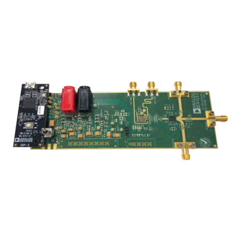
Figure 2. Default Evaluation Board Configuration
Downloaded from Arrow.com.Downloaded from Arrow.com.Downloaded from Arrow.com.
