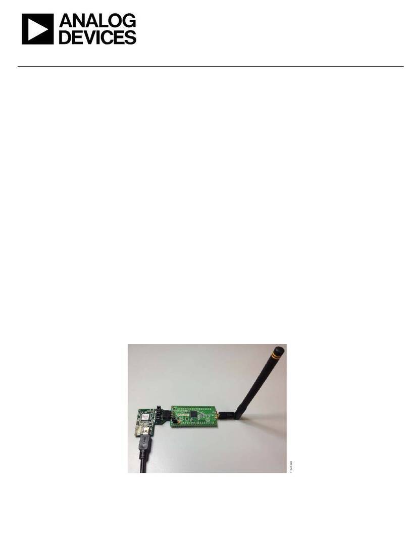
UG-XXX Evaluation Board User Guide
EVALUATION BOARD HARDWARE
DEVICE DESCRIPTION
The AD7124-8 is a low power, low noise, complete analog front
end for high precision measurement applications. It contains a
low noise, 24-bit Σ-Δ ADC. It can be configured to have four
differential inputs or seven single-ended or pseudo-differential
inputs. The on-chip low noise instrumentation amplifier means
that signals of small amplitude can be interfaced directly to the
ADC. Other on-chip features include a low drift 2.5 V
reference, excitation currents, reference buffers, multiple filter
options and many diagnostic features.
Complete specifications for the AD7124-8 are provided in the
product data sheet and should be consulted in conjunction with
this user guide when using the evaluation board. Full details
about the EVAL-SDP-CB1Z are available on the Analog
Devices, Inc., website.
HARDWARE LINK OPTIONS
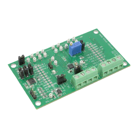
The default link options are listed in Table 1. By default, the
board is configured to operate from a wall wart (dc plug) power
supply via Connector J5. The supply required for the AD7124-8
comes from the on-board ADP1720 LDOs, which generate their
input voltage from J5.
Table 1. Default Link and Solder Link Options
Link No.
Default
Option
Description
LK1 A Connects the AVDD voltage to the power supply sequencer, ADM1185.
When AVDD equals 3.3 V, LK1 must be in Position A.
When AVDD equals 1.8 V, LK1 must be in Position B.
LK2 B Selects the connector for the external 7 V to 9 V power supply.
In Position A, this link selects the external 7 V to 9 V power supply to come from Connector J3.
In Position B, this link selects the external 7 V to 9 V power supply to come from Connector J5.
LK3 Inserted Inserting this link connects REFIN(-) to AVSS.
LK4 2.5 V Selects the reference source for the ADC.
In position 2.5V, REFIN1(+) is connected to the external 2.5 V reference (ADR4525).
In position INT REF, REFIN1(+) is connected to the REFOUT pin of the AD7124-8. The AD7124-8’s internal
reference can be enabled and applied to the AD7124-8 external to the ADC.
LK5
This link shorts AIN0 to AIN1. This is useful to perform noise tests on the AD7124-8. The internal bias can
be enabled on AIN0 or AIN1 so that AIN0 and AIN1 are at an appropriate voltage for the noise test.
Headers J13 and J14 can be used to connect channels AIN4 and AIN5 to external components such as an
external amplifier. Both links at LK6 should be opened to include the external component on the front-
SL2 A Sets the voltage applied to the AVDD pin.
In Position A, this link sets the voltage applied to the AVDD pin to be a 3.3 V supply from the ADP1720-3.3
(U7) regulator or a 2.5 V supply from the ADP1720 (U4) regulator.
In Position B, this link sets the voltage applied to the AVDD pin to be supplied from an external voltage
source via Connector J9.
SL3, SL7 A, A With SL3 and SL7 in Position A, AVDD is supplied with 3.3 V from ADP1720-3.3 (U7) regulator.
With SL3 and SL7 in Position B, AVDD is supplied with 1.8 V from the ADP1720 (U4) regulator.
SL5 B With this link in Position A, the IOVDD supply is provided from an external source via Connector J9.
With this link in Position B, the 3.3 V supply is generated by the ADP1720-3.3 (U10) regulator.
The evaluation system operates with 3.3 V logic.
AVSS to
AGND
R49, R50, R51,
R52
When these links are inserted, AVSS is tied to AGND. When AVSS is set to −1.8 V, these links must be
removed.
Rev. PrA | Page 4 of 36
