Analog Devices ADG5412BF User manual

Bidirectional Fault Protection and
Detection, 10 Ω RON, Quad SPST Switches
Data Sheet ADG5412BF/ADG5413BF
Rev. B Document Feedback
Information furnished by Analog Devices is believed to be accurate and reliable. However, no
responsibility is assumed by Analog Devices for its use, nor for any infringements of patents or other
rights of thirdparties thatmay result from its use. Specifications subject to changewithout notice. No
license is granted by implication or otherwise under any patent or patent rights of Analog Devices.
Trademarks andregistered trademarks are the property of their respective owners.
One Technology Way, P.O. Box 9106, Norwood, MA 02062-9106, U.S.A.
Tel: 781.329.4700 ©2014–2016 Analog Devices, Inc. All rights reserved.
Technical Support www.analog.com
FEATURES
Overvoltage protection up to −55 V and +55 V
Power-off protection up to −55 V and +55 V
Overvoltage detection on source and drain pins
Low on resistance: 10 Ω
On-resistance flatness of 0.5 Ω
3 kV human body model (HBM) ESD rating
Latch-up immune under any circumstance
Known state without digital inputs present
VSS to VDD analog signal range
±5 V to ±22 V dual-supply operation
8 V to 44 V single-supply operation
Fully specified at ±15 V, ±20 V, +12 V, and +36 V
APPLICATIONS
Analog input/output modules
Process control/distributed control systems
Data acquisition
Instrumentation
Avionics
Automatic test equipment
Communication systems
Relay replacement
FUNCTIONAL BLOCK DIAGRAMS
NOTES
1. SWITCHES SHOWN FOR A LOGIC 1 INPUT.
D1
D2
D3
D4
S1
S2
S3
S4
ADG5412BF
FF
FAULT
DETECTION
+ SWITCH
DRIVER
IN1 IN2 IN3 IN4
12473-001
Figure 1. ADG5412BF
NOTES
1. SWITCHES SHOWN FOR A LOGIC 1 INPUT.
IN1
D1
IN2
D2
IN3
D3
IN4
D4
S1
S2
S3
S4
ADG5413BF
FF
FAULT
DETECTION
+ SWITCH
DRIVER
12473-200
Figure 2. ADG5413BF
GENERAL DESCRIPTION
The ADG5412BF and ADG5413BF contain four independently
controlled single-pole/single-throw (SPST) switches. The
ADG5412BF has four switches that turn on with Logic 1 inputs.
The ADG5413BF has two switches that turn on and two switches
that turn off with Logic 1 inputs. Each switch conducts equally
well in both directions when on, and each switch has an input
signal range that extends to the supplies. The digital inputs are
compatible with 3 V logic inputs over the full operating supply
range.
When no power supplies are present, the switch remains in the
off condition, and the switch inputs are high impedance. Under
normal operating conditions, if the analog input signal levels on
any switch pin exceed VDD or VSS by a threshold voltage, VT, the
switch turns off. Input signal levels up to +55 V and −55 V relative
to ground are blocked, in both the powered and unpowered
condition.
The low on resistance of these switches, combined with on-
resistance flatness over a significant portion of the signal range
make them an ideal solution for data acquisition and gain switching
applications where excellent linearity and low distortion are critical.
PRODUCT HIGHLIGHTS
1. Switch pins are protected against voltages greater than the
supply rails, up to −55 V and +55 V.
2. Switch pins are protected against voltages between −55 V
and +55 V, in an unpowered state.
3. Overvoltage detection with digital output indicates
operating state of switches.
4. Trench isolation guards against latch-up.
5. Optimized for low on resistance and on-resistance flatness.
6. The ADG5412BF/ADG5413BF can be operated from a
dual-supply of ±5 V up to ±22 V or a single power supply
of 8 V up to 44 V.
ADG5412BF/ADG5413BF Data Sheet
Rev. B | Page 2 of 28
TABLE OF CONTENTS
Features .............................................................................................. 1
Applications....................................................................................... 1
Functional Block Diagrams............................................................. 1
General Description......................................................................... 1
Product Highlights ........................................................................... 1
Revision History ............................................................................... 2
Specifications..................................................................................... 3
±15 V Dual-Supply....................................................................... 3
±20 V Dual-Supply....................................................................... 5
12 V Single-Supply ....................................................................... 7
36 V Single-Supply ....................................................................... 9
Continuous Current per Channel, Sx or Dx........................... 11
Absolute Maximum Ratings.......................................................... 12
ESD Caution................................................................................ 12
Pin Configuration and Function Descriptions........................... 13
Typical Performance Characteristics ........................................... 14
Test Circuits..................................................................................... 19
Terminology .................................................................................... 23
Theory of Operation ...................................................................... 25
Switch Architecture.................................................................... 25
Fault Protection .......................................................................... 26
Applications Information .............................................................. 27
Power Supply Rails..................................................................... 27
Power Supply Sequencing Protection...................................... 27
Signal Range................................................................................ 27
Low Impedance Channel Protection ....................................... 27
High Voltage Surge Suppression .............................................. 27
Intelligent Fault Detection ........................................................ 27
Large Voltage, High Frequency Signals................................... 27
Outline Dimensions....................................................................... 28
Ordering Guide .......................................................................... 28
REVISION HISTORY
1/16—Rev. A to Rev. B
Changes to Table 1............................................................................ 3
Changes to Table 2............................................................................ 5
Changes to Table 3............................................................................ 7
Changes to Table 4............................................................................ 9
Changes to Switch Architecture Section ..................................... 25
3/15—Rev. 0 to Rev. A
Added LFCSP Package.......................................................Universal
Changes to Output Leakage Current, ISor ID/With Overvoltage
Parameter, Table 3............................................................................. 7
Changes to Output Leakage Current, ISor ID/With Overvoltage
Parameter, Table 4............................................................................. 9
Changes to Table 6.......................................................................... 12
Added Figure 4, Renumbered Sequentially ................................ 13
Changes to Table 7.......................................................................... 13
Changes to Figure 35...................................................................... 19
Changes to Figure 50...................................................................... 25
Changes to Applications Information Section ........................... 27
Updated Outline Dimensions....................................................... 28
Changes to Ordering Guide.......................................................... 28
7/14—Revision 0: Initial Version

Data Sheet ADG5412BF/ADG5413BF
Rev. B | Page 3 of 28
SPECIFICATIONS
±15 V DUAL-SUPPLY
VDD = 15 V ± 10%, VSS = −15 V ± 10%, GND = 0 V, CDECOUPLING = 0.1 μF, unless otherwise noted.
Table 1.
Parameter +25°C
−40°C to
+85°C
−40°C to
+125°C Unit Test Conditions/Comments
ANALOG SWITCH VDD = 13.5 V, VSS = −13.5 V, see Figure 32
Analog Signal Range VDD to VSS V
On Resistance, RON 10 Ω typ VS= ±10 V, IS= −10 mA
11.2 14 16.5 Ω max
9.5 Ω typ VS= ±9 V, IS= −10 mA
10.7 13.5 16 Ω max
On-Resistance Match Between Channels, ∆RON 0.05 Ω typ VS= ±10 V, IS= −10 mA
0.5 0.6 0.7 Ω max
0.05 Ω typ VS= ±9 V, IS= −10 mA
0.35 0.5 0.5 Ω max
On-Resistance Flatness, RFLAT(ON) 0.6 Ω typ VS= ±10 V, IS= −10 mA
0.9 1.1 1.1 Ω max
0.1 Ω typ VS= ±9 V, IS= −10 mA
0.4 0.5 0.5 Ω max
Threshold Voltage, VT0.7 V typ See Figure 28
LEAKAGE CURRENTS VDD = 16.5 V, VSS = −16.5 V
Source Off Leakage, IS(Off) ±0.1 nA typ VS= ±10 V, VD= ∓10 V, see Figure 33
±1.5 ±5.5 ±24 nA max
Drain Off Leakage, ID(Off) ±0.1 nA typ VS= ±10 V, VD= ∓10 V, see Figure 33
±1.5 ±5.5 ±20 nA max
Channel On Leakage, ID(On), IS(On) ±0.3 nA typ VS= VD= ±10 V, see Figure 34
±2.0 ±2.5 ±5.5 nA max
FAULT
Input Leakage Current, ISor ID
With Overvoltage ±78 μA typ VDD = 16.5 V, VSS = 16.5 V, GND = 0 V, VS
or VD= ±55 V, see Figure 37
Power Supplies Grounded or Floating ±40 μA typ VDD = 0 V or floating, VSS = 0 V or
floating, GND = 0 V, INx = 0 V or
floating, VSor VD= ±55 V, see Figure 38
Output Leakage Current, ISor ID
With Overvoltage ±20 nA typ VDD = 16.5 V, VSS = 16.5 V, GND = 0 V, VS
or VD= ±55 V, see Figure 37
±200 ±250 ±250 nA max
Power Supplies Grounded ±10 nA typ VDD = 0 V, VSS = 0 V, GND = 0 V, VSor VD=
±55 V, INx = 0 V, see Figure 38
±30 ±50 ±100 nA max
Power Supplies Floating ±10 ±10 ±10 μA typ VDD = floating, VSS = floating, GND = 0 V,
VSor VD= ±55 V, INx = 0 V, see Figure 38
DIGITAL INPUTS/OUTPUTS
Input Voltage
High, VINH 2.0 V min
Low, VINL 0.8 V max
Input Current, IINL or IINH ±0.7 μA typ VIN = VGND or VDD
±1.2 μA max
Digital Input Capacitance, CIN 5.0 pF typ

ADG5412BF/ADG5413BF Data Sheet
Rev. B | Page 4 of 28
Parameter +25°C
−40°C to
+85°C
−40°C to
+125°C Unit Test Conditions/Comments
Output Voltage V min
High, VOH 2.0 V min
Low, VOL 0.8 V max
DYNAMIC CHARACTERISTICS1
tON 400 ns typ RL= 300 Ω, CL= 35 pF
495 525 550 ns max VS= 10 V, see Figure 47
tOFF 410 ns typ RL= 300 Ω, CL= 35 pF
510 545 555 ns max VS= 10 V, see Figure 47
Break-Before-Make Time Delay, tD
(ADG5413BF Only)
285 ns typ RL= 300 Ω, CL= 35 pF
185 ns min VS1 = VS2 = 10 V, see Figure 46
Overvoltage Response Time, tRESPONSE 460 ns typ RL= 1 kΩ, CL= 2 pF, see Figure 41
585 615 630 ns max
Overvoltage Recovery Time, tRECOVERY 720 ns typ RL= 1 kΩ, CL= 2 pF, see Figure 42
930 1050 1100 ns max
Interrupt Flag Response Time, tDIGRESP 85 115 ns typ CL= 10 pF, see Figure 43
Interrupt Flag Recovery Time, tDIGREC 60 85 μs typ CL= 10 pF, see Figure 44
600 ns typ
CL= 10 pF, RPULLUP = 1 kΩ, see
Figure 45
Charge Injection, QINJ −680 pC typ VS= 0 V, RS= 0 Ω, CL= 1 nF, see Figure 48
Off Isolation −70 dB typ RL= 50 Ω, CL= 5 pF, f = 1 MHz, see
Figure 35
Channel-to-Channel Crosstalk −90 dB typ RL= 50 Ω, CL= 5 pF, f = 1 MHz, see
Figure 36
Total Harmonic Distortion Plus Noise,THD + N 0.0015 % typ RL= 10 kΩ, VS= 15 V p-p, f = 20 Hz to
20 kHz, see Figure 40
−3 dB Bandwidth 270 MHz typ RL= 50 Ω, CL= 5 pF, see Figure 39
Insertion Loss −0.72 dB typ RL= 50 Ω, CL= 5 pF, f = 1 MHz, see
Figure 39
CS(Off) 13 pF typ VS= 0 V, f = 1 MHz
CD(Off) 12 pF typ VS= 0 V, f = 1 MHz
CD(On), CS(On) 24 pF typ VS= 0 V, f = 1 MHz
POWER REQUIREMENTS VDD = 16.5 V, VSS = −16.5 V, digital inputs =
0 V, 5 V, or VDD
Normal Mode
IDD 0.9 mA typ
1.2 1.3 mA max
IGND 0.4 mA typ
0.55 0.6 mA max
ISS 0.5 mA typ
0.65 0.7 μA max
Fault Mode VS= ±55 V
IDD 1.2 mA typ
1.6 1.8 mA max
IGND 0.8 mA typ
1.0 1.1 mA max
ISS 0.5 mA typ
1.0 1.8 mA max
VDD/VSS ±5 V min GND = 0 V
±22 V max GND = 0 V
1Guaranteed by design; not subject to production test.

Data Sheet ADG5412BF/ADG5413BF
Rev. B | Page 5 of 28
±20 V DUAL-SUPPLY
VDD = 20 V ± 10%, VSS = −20 V ± 10%, GND = 0 V, CDECOUPLING = 0.1 μF, unless otherwise noted.
Table 2.
Parameter +25°C
−40°C to
+85°C
−40°C to
+125°C Unit Test Conditions/Comments
ANALOG SWITCH VDD = 18 V, VSS = −18 V, see
Figure 32
Analog Signal Range VDD to VSS V
On Resistance, RON 10 Ω typ VS= ±15 V, IS= −10 mA
11.5 14.5 16.5 Ω max
9.5 Ω typ VS= ±13.5 V, IS= −10 mA
11 14 16.5 Ω max
On-Resistance Match Between Channels, ∆RON 0.05 Ω typ VS= ±15 V, IS= −10 mA
0.35 0.5 0.5 Ω max
0.05 Ω typ VS= ±13.5 V, IS= −10 mA
0.35 0.5 0.5 Ω max
On-Resistance Flatness, RFLAT(ON) 1.0 Ω typ VS= ±15 V, IS= −10 mA
1.4 1.5 1.5 Ω max
0.1 Ω typ VS= ±13.5 V, IS= −10 mA
0.4 0.5 0.5 Ω max
Threshold Voltage, VT0.7 V typ See Figure 28
LEAKAGE CURRENTS VDD = 22 V, VSS = −22 V
Source Off Leakage, IS(Off) ±0.1 nA typ VS= ±15 V, VD= ∓15 V, see Figure 33
±1.5 ±5.5 ±24 nA max
Drain Off Leakage, ID(Off) ±0.1 nA typ VS= ±15 V, VD= ∓15 V, see Figure 33
±1.5 ±5.5 ±20 nA max
Channel On Leakage, ID(On), IS(On) ±0.3 nA typ VS= VD= ±15 V, see Figure 34
±2.0 ±2.5 ±5.5 nA max
FAULT
Input Leakage Current, ISor ID
With Overvoltage ±78 μA typ VDD = 22 V, VSS = −22 V, GND = 0 V,
VSor VD= ±55 V, see Figure 37
Power Supplies Grounded or Floating ±40 μA typ VDD = 0 V or floating, VSS = 0 V or
floating, GND = 0 V, INx = 0 V or
floating, VSor VD= ±55 V, see
Figure 38
Output Leakage Current, ISor ID
With Overvoltage ±0.4 μA typ VDD = +22 V, VSS = −22 V, GND = 0 V,
VSor VD= ±55 V, see Figure 37
±1.0 ±1.0 ±1.0 μA max
Power Supplies Grounded ±10 nA typ VDD = 0 V, VSS = 0 V, GND = 0 V, VSor
VD= ±55 V, INx = 0 V, see Figure 38
±30 ±50 ±100 nA max
Power Supplies Floating ±10 ±10 ±10 μA typ VDD = floating, VSS = floating, GND
= 0 V, VSor VD= ±55 V, INx = 0 V,
see Figure 38
DIGITAL INPUTS
Input Voltage
High, VINH 2.0 V min
Low, VINL 0.8 V max
Input Current, IINL or IINH 0.7 μA typ VIN = VGND or VDD
1.2 μA max
Digital Input Capacitance, CIN 5.0 pF typ

ADG5412BF/ADG5413BF Data Sheet
Rev. B | Page 6 of 28
Parameter +25°C
−40°C to
+85°C
−40°C to
+125°C Unit Test Conditions/Comments
Output Voltage
High, VOH 2.0 V min
Low, VOL 0.8 V max
DYNAMIC CHARACTERISTICS1
tON 400 ns typ RL= 300 Ω, CL= 35 pF
500 530 555 ns max VS= 10 V, see Figure 47
tOFF 415 ns typ RL= 300 Ω, CL= 35 pF
515 550 565 ns max VS= 10 V, see Figure 47
Break-Before-Make Time Delay, tD
(ADG5413BF Only)
295 ns typ RL= 300 Ω, CL= 35 pF
200 ns min VS1 = VS2 = 10 V, see Figure 46
Overvoltage Response Time, tRESPONSE 370 ns typ RL= 1 kΩ, CL= 2 pF, see Figure 41
480 500 515 ns max
Overvoltage Recovery Time, tRECOVERY 840 ns typ RL= 1 kΩ, CL= 2 pF, see Figure 42
1200 1400 1700 ns max
Interrupt Flag Response Time, tDIGRESP 85 115 ns typ CL= 10 pF, see Figure 43
Interrupt Flag Recovery Time, tDIGREC 60 85 μs typ CL= 10 pF, see Figure 44
600 ns typ
CL= 10 pF, RPULLUP = 1 kΩ, see
Figure 45
Charge Injection, QINJ −640 pC typ
VS= 0 V, RS= 0 Ω, CL= 1 nF, see
Figure 48
Off Isolation −70 dB typ RL= 50 Ω, CL= 5 pF, f = 1 MHz, see
Figure 35
Channel-to-Channel Crosstalk −90 dB typ RL= 50 Ω, CL= 5 pF, f = 1 MHz, see
Figure 36
Total Harmonic Distortion Plus Noise, THD + N 0.001 % typ RL= 10 kΩ, VS= 20 V p-p, f = 20 Hz
to 20 kHz, see Figure 40
−3 dB Bandwidth 270 MHz typ RL= 50 Ω, CL= 5 pF, see Figure 39
Insertion Loss −0.73 dB typ RL= 50 Ω, CL= 5 pF, f = 1 MHz, see
Figure 39
CS(Off) 12 pF typ VS= 0 V, f = 1 MHz
CD(Off) 11 pF typ VS= 0 V, f = 1 MHz
CD(On), CS(On) 23 pF typ VS= 0 V, f = 1 MHz
POWER REQUIREMENTS VDD = 22 V, VSS = −22 V, digital
inputs = 0 V, 5 V, or VDD
Normal Mode
IDD 0.9 mA typ
1.2 1.3 mA max
IGND 0.4 mA typ
0.55 0.6 mA max
ISS 0.5 mA typ
0.65 0.7 mA max
Fault Mode VS= ±55 V
IDD 1.2 mA typ
1.6 1.8 mA max
IGND 0.8 mA typ
1.0 1.1 mA max
ISS 0.5 mA typ
1.0 1.8 mA max
VDD/VSS ±5 V min GND = 0 V
±22 V max GND = 0 V
1Guaranteed by design; not subject to production test.

Data Sheet ADG5412BF/ADG5413BF
Rev. B | Page 7 of 28
12 V SINGLE-SUPPLY
VDD = 12 V ± 10%, VSS = 0 V, GND = 0 V, CDECOUPLING = 0.1 μF, unless otherwise noted.
Table 3.
Parameter +25°C
−40°C to
+85°C
−40°C to
+125°C Unit Test Conditions/Comments
ANALOG SWITCH VDD = 10.8 V, VSS = 0 V, see Figure 32
Analog Signal Range 0 V to VDD V
On Resistance, RON 22 Ω typ VS= 0 V to 10 V, IS= −10 mA
24.5 31 37 Ω max
10 Ω typ VS= 3.5 V to 8.5 V, IS= −10 mA
11.2 14 16.5 Ω max
On-Resistance Match Between Channels, ∆RON 0.05 Ω typ VS= 0 V to 10 V, IS= −10 mA
0.5 0.6 0.7 Ω max
0.05 Ω typ VS= 3.5 V to 8.5 V, IS= −10 mA
0.5 0.6 0.7 Ω max
On-Resistance Flatness, RFLAT(ON) 12.5 Ω typ VS= 0 V to 10 V, IS= −10 mA
14.5 19 23 Ω max
0.6 Ω typ VS= 3.5 V to 8.5 V, IS= −10 mA
0.9 1.1 1.3 Ω max
Threshold Voltage, VT0.7 V typ See Figure 28
LEAKAGE CURRENTS VDD = 13.2 V, VSS = 0 V
Source Off Leakage, IS(Off) ±0.1 nA typ VS= 1 V/10 V, VD= 10 V/1 V, see Figure 33
±1.5 ±5.5 ±24 nA max
Drain Off Leakage, ID(Off) ±0.1 nA typ VS= 1 V/10 V, VD= 10 V/1 V, see Figure 33
±1.5 ±5.5 ±20 nA max
Channel On Leakage, ID(On), IS(On) ±0.3 nA typ VS= VD= 1 V/10 V, see Figure 34
±2.0 ±2.5 ±5.5 nA max
FAULT
Input Leakage Current, ISor ID
With Overvoltage ±78 μA typ VDD = 13.2 V, VSS = 0 V, GND = 0 V, VSor
VD= ±55 V, see Figure 37
Power Supplies Grounded or Floating ±40 μA typ VDD = 0 V or floating, VSS = 0 V or floating,
GND = 0 V, INx = 0 V or floating, VSor
VD= ±55 V, see Figure 38
Output Leakage Current, ISor ID
With Overvoltage ±20 nA typ VDD = 13.2 V, VSS = 0 V, GND = 0 V, VSor
VD= ±55 V, see Figure 37
±200 ±250 ±250 nA max
Power Supplies Grounded ±10 nA typ VDD = 0 V, VSS = 0 V, GND = 0 V, VSor VD=
±55 V, INx = 0 V, see Figure 38
±30 ±50 ±100 nA max
Power Supplies Floating ±10 ±10 ±10 μA typ VDD = floating, VSS = floating, GND = 0 V,
VSor VD= ±55 V, INx = 0 V, see Figure 38
DIGITAL INPUTS
Input Voltage
High, VINH 2.0 V min
Low, VINL 0.8 V max
Input Current, IINL or IINH 0.7 μA typ VIN = VGND or VDD
1.2 μA max
Digital Input Capacitance, CIN 5.0 pF typ
Output Voltage
High, VOH 2.0 V min
Low, VOL 0.8 V max

ADG5412BF/ADG5413BF Data Sheet
Rev. B | Page 8 of 28
Parameter +25°C
−40°C to
+85°C
−40°C to
+125°C Unit Test Conditions/Comments
DYNAMIC CHARACTERISTICS1
tON 400 ns typ RL= 300 Ω, CL= 35 pF
485 515 540 ns max VS= 8 V, see Figure 47
tOFF 375 ns typ RL= 300 Ω, CL= 35 pF
460 495 520 ns max VS= 8 V, see Figure 47
Break-Before-Make Time Delay, tD
(ADG5413BF Only)
260 ns typ RL= 300 Ω, CL= 35 pF
170 ns min VS1 = VS2 = 8 V, see Figure 46
Overvoltage Response Time, tRESPONSE 560 ns typ RL= 1 kΩ, CL= 2 pF, see Figure 41
660 700 720 ns max
Overvoltage Recovery Time, tRECOVERY 640 ns typ RL= 1 kΩ, CL= 2 pF, see Figure 42
800 865 960 ns max
Interrupt Flag Response Time, tDIGRESP 85 115 ns typ CL= 10 pF, see Figure 43
Interrupt Flag Recovery Time, tDIGREC 60 85 μs typ CL= 10 pF, see Figure 44
600 ns typ CL= 10 pF, RPULLUP = 1 kΩ, see Figure 45
Charge Injection, QINJ −340 pC typ VS= 6 V, RS= 0 Ω, CL= 1 nF, see Figure 48
Off Isolation −65 dB typ RL= 50 Ω, CL= 5 pF, f = 1 MHz, see
Figure 35
Channel-to-Channel Crosstalk −90 dB typ RL= 50 Ω, CL= 5 pF, f = 1 MHz, see
Figure 36
Total Harmonic Distortion Plus Noise, THD + N 0.007 % typ RL= 10 kΩ, VS= 6 V p-p, f = 20 Hz to
20 kHz, see Figure 40
−3 dB Bandwidth 270 MHz typ RL= 50 Ω, CL= 5 pF, see Figure 39
Insertion Loss −0.74 dB typ RL= 50 Ω, CL= 5 pF, f = 1 MHz, see
Figure 39
CS(Off) 16 pF typ VS= 6 V, f = 1 MHz
CD(Off) 15 pF typ VS= 6 V, f = 1 MHz
CD(On), CS(On) 25 pF typ VS= 6 V, f = 1 MHz
POWER REQUIREMENTS VDD = 13.2 V, VSS = 0 V, digital inputs = 0 V,
5 V, or VDD
Normal Mode
IDD 0.9 mA typ
1.2 1.3 mA max
IGND 0.4 mA typ
0.55 0.6 mA max
ISS 0.5 mA typ
0.65 0.7 mA max
Fault Mode VS= ±55 V
IDD 1.2 mA typ
1.6 1.8 mA max
IGND 0.8 mA typ
1.0 1.1 mA max
ISS 0.5 mA typ
1.0 1.8 mA max
VDD 8 V min VSS = GND = 0 V
44 V max VSS = GND = 0 V
1Guaranteed by design; not subject to production test.

Data Sheet ADG5412BF/ADG5413BF
Rev. B | Page 9 of 28
36 V SINGLE-SUPPLY
VDD = 36 V ± 10%, VSS = 0 V, GND = 0 V, CDECOUPLING = 0.1 μF, unless otherwise noted.
Table 4.
Parameter +25°C
−40°C to
+85°C
−40°C to
+125°C Unit Test Conditions/Comments
ANALOG SWITCH VDD = 32.4 V, VSS = 0 V, see Figure 32
Analog Signal Range 0 V to VDD V
On Resistance, RON 22 Ω typ VS= 0 V to 30 V, IS= −10 mA
24.5 31 37 Ω max
10 Ω typ VS= 4.5 V to 28 V, IS= −10 mA
11 14 16.5 Ω max
On-Resistance Match Between Channels, ∆RON 0.05 Ω typ VS= 0 V to 30 V, IS= −10 mA
0.5 0.6 0.7 Ω max
0.05 Ω typ VS= 4.5 V to 28 V, IS= −10 mA
0.35 0.5 0.5 Ω max
On-Resistance Flatness, RFLAT(ON) 12.5 Ω typ VS= 0 V to 30 V, IS= −10 mA
14.5 19 23 Ω max
0.1 Ω typ VS= 4.5 V to 28 V, IS= −10 mA
0.4 0.5 0.5 Ω max
Threshold Voltage, VT0.7 V typ See Figure 28
LEAKAGE CURRENTS VDD = 39.6 V, VSS = 0 V
Source Off Leakage, IS(Off) ±0.1 nA typ VS= 1 V/30 V, VD= 30 V/1 V, see
Figure 33
±1.5 ±5.5 ±24 nA max
Drain Off Leakage, ID(Off) ±0.1 nA typ VS= 1 V/30 V, VD= 30 V/1 V, see
Figure 33
±1.5 ±5.5 ±20 nA max
Channel On Leakage, ID(On), IS(On) ±0.3 nA typ VS= VD= 1 V/30 V, see Figure 34
±2.0 ±2.5 ±5.5 nA max
FAULT
Input Leakage Current, ISor ID
With Overvoltage ±78 μA typ VDD = 39.6 V, VSS = 0 V, GND = 0 V, VSor
VD= +55 V, −40 V, see Figure 37
Power Supplies Grounded or Floating ±40 μA typ VDD = 0 V or floating, VSS = 0 V or
floating, GND = 0 V, INx = 0 V or
floating, VSor VD= ±55 V, see Figure 38
Output Leakage Current, ISor ID
With Overvoltage ±20 nA typ VDD = 39.6 V, VSS = 0 V, GND = 0 V, VSor
VD= +55 V, −40 V, see Figure 37
±200 ±250 ±250 nA max
Power Supplies Grounded ±10 nA typ VDD = 0 V, VSS = 0 V, GND = 0 V, VSor
VD= ±55 V, INx = 0 V, see Figure 38
±30 ±50 ±100 nA max
Power Supplies Floating ±10 ±10 ±10 μA typ VDD = floating, VSS = floating, GND =
0 V, VSor VD= ±55 V, INx = 0 V, see
Figure 38
DIGITAL INPUTS
Input Voltage
High, VINH 2.0 V min
Low, VINL 0.8 V max
Input Current, IINL or IINH 0.7 μA typ VIN = VGND or VDD
1.2 μA max
Digital Input Capacitance, CIN 5.0 pF typ

ADG5412BF/ADG5413BF Data Sheet
Rev. B | Page 10 of 28
Parameter +25°C
−40°C to
+85°C
−40°C to
+125°C Unit Test Conditions/Comments
Output Voltage
High, VOH 2.0 V min
Low, VOL 0.8 V max
DYNAMIC CHARACTERISTICS1
tON 400 ns typ RL= 300 Ω, CL= 35 pF
490 520 545 ns max VS= 18 V, see Figure 47
tOFF 375 ns typ RL= 300 Ω, CL= 35 pF
460 485 510 ns max VS= 18 V, see Figure 47
Break-Before-Make Time Delay, tD
(ADG5413BF Only)
285 ns typ RL= 300 Ω, CL= 35 pF
195 ns min VS1 = VS2 = 18 V, see Figure 46
Overvoltage Response Time, tRESPONSE 250 ns typ RL= 1 kΩ, CL= 2 pF, see Figure 41
350 360 375 ns max
Overvoltage Recovery Time, tRECOVERY 1500 ns typ RL= 1 kΩ, CL= 2 pF, see Figure 42
2000 2300 2700 ns max
Interrupt Flag Response Time, tDIGRESP 85 115 ns typ CL= 10 pF, see Figure 43
Interrupt Flag Recovery Time, tDIGREC 60 85 μs typ CL= 10 pF, see Figure 44
600 ns typ CL= 10 pF, RPULLUP = 1 kΩ, see Figure 45
Charge Injection, QINJ −610 pC typ
VS= 18 V, RS= 0 Ω, CL= 1 nF, see
Figure 48
Off Isolation −70 dB typ RL= 50 Ω, CL= 5 pF, f = 1 MHz, see
Figure 35
Channel-to-Channel Crosstalk −90 dB typ RL= 50 Ω, CL= 5 pF, f = 1 MHz, see
Figure 36
Total Harmonic Distortion Plus Noise, THD + N 0.001 % typ RL= 10 kΩ, VS= 18 V p-p, f = 20 Hz to
20 kHz, see Figure 40
−3 dB Bandwidth 270 MHz typ RL= 50 Ω, CL= 5 pF, see Figure 39
Insertion Loss −0.75 dB typ RL= 50 Ω, CL= 5 pF, f = 1 MHz, see
Figure 39
CS(Off) 12 pF typ VS= 18 V, f = 1 MHz
CD(Off) 11 pF typ VS= 18 V, f = 1 MHz
CD(On), CS(On) 23 pF typ VS= 18 V, f = 1 MHz
POWER REQUIREMENTS VDD = 39.6 V, VSS = 0 V, digital inputs =
0 V, 5 V, or VDD
Normal Mode
IDD 0.9 mA typ
1.2 1.3 mA max
IGND 0.4 mA typ
0.55 0.6 mA max
ISS 0.5 mA typ
0.65 0.7 mA max
Isolation Mode VS= +55 V, −40 V
IDD 1.2 mA typ
1.6 1.8 mA max
IGND 0.8 mA typ
1.0 1.1 mA max
ISS 0.5 mA typ
1.0 1.8 mA max
VDD 8 V min VSS = GND = 0 V
44 V max VSS = GND = 0 V
1Guaranteed by design; not subject to production test.

Data Sheet ADG5412BF/ADG5413BF
Rev. B | Page 11 of 28
CONTINUOUS CURRENT PER CHANNEL, Sx OR Dx
Table 5.
Parameter 25°C 85°C 125°C Unit Test Conditions/Comments
16-LEAD TSSOP
θJA = 112.6°C/W 83 59 39 mA max VS= VSS + 4.5 V to VDD − 4.5 V
64 48 29 mA max VS= VSS to VDD
16-LEAD LFCSP
θJA = 30.4°C/W 152 99 61 mA max VS= VSS + 4.5 V to VDD − 4.5 V
118 80 52 mA max VS= VSS to VDD

ADG5412BF/ADG5413BF Data Sheet
Rev. B | Page 12 of 28
ABSOLUTE MAXIMUM RATINGS
TA= 25°C, unless otherwise noted.
Table 6.
Parameter Rating
VDD to VSS 48 V
VDD to GND −0.3 V to +48 V
VSS to GND −48 V to +0.3 V
Sx and Dx −55 V to +55 V
Sx to VDD or VSS 80 V
VSto VD80 V
Digital Inputs GND − 0.7 V to +48 V or 30 mA,
whichever occurs first
Peak Current, Sx or Dx Pins 288 mA (pulsed at 1 ms, 10%
duty cycle maximum)
Continuous Current, Sx or Dx
Pins
Data1+ 15%
Digital Output GND − 0.7 V to 6 V or 30 mA,
whichever occurs first
Operating Temperature
Range
−40°C to +125°C
Storage Temperature Range −65°C to +150°C
Junction Temperature 150°C
Thermal Impedance, θJA
(4-Layer Board)
16-Lead TTSOP 112.6°C/W
16-Lead LFSCP 30.4°C/W
Reflow Soldering Peak
Temperature, Pb Free
As per JEDEC J-STD-020
ESD (HBM: ANSI/ESD
STM5.1-2007)
I/O Port to Supplies 5.5 kV
I/O Port to I/O Port 5.5 kV
All Other Pins 3 kV
1See Table 5.
Stresses at or above those listed under Absolute Maximum
Ratings may cause permanent damage to the product. This is a
stress rating only; functional operation of the product at these
or any other conditions above those indicated in the operational
section of this specification is not implied. Operation beyond
the maximum operating conditions for extended periods may
affect product reliability.
Only one absolute maximum rating can be applied at any one time.
ESD CAUTION

Data Sheet ADG5412BF/ADG5413BF
Rev. B | Page 13 of 28
PIN CONFIGURATION AND FUNCTION DESCRIPTIONS
1
2
3
4
5
6
7
8
16
15
14
13
12
11
10
9
D1
S1
V
SS
D4
S4
GND
IN1
D2
S2
V
DD
D3
IN4 IN3
S3
FF
IN2
ADG5412BF/
ADG5413BF
TOP VIEW
(Not to Scale)
12473-003
Figure 3. TSSOP Pin Configuration
12473-104
12
11
10
1
3
49
2
6
5
7
8
16
15
14
13
NOTES
1. THE EXPOSED PAD IS INTERNALLY CONNECTED.
FOR INCREASED RELIABILITY OF THE SOLDER JOINTS
AND MAXIMUM THERMAL CAPABILITY, IT IS RECOMMENDED
THAT THE PAD BE CONNECTED TO THE LOWEST SUPPLY VOLTAGE, V
SS
.
S1
V
SS
GND
S4
S2
D2
IN
2
IN1
D1
V
DD
FF
S3
D4
IN4
IN3
D3
ADG5412BF/
ADG5413BF
TOP VIEW
Figure 4. LFCSP Pin Configuration
Table 7. Pin Function Descriptions
Pin No.
Mnemonic Description
TSSOP LFCSP
1 15 IN1 Logic Control Input.
2 16 D1 Overvoltage Protected Drain Terminal. This pin can be an input or an output.
3 1 S1 Overvoltage Protected Source Terminal. This pin can be an input or an output.
4 2 VSS Most Negative Power Supply Potential.
5 3 GND Ground (0 V) Reference.
6 4 S4 Overvoltage Protected Source Terminal. This pin can be an input or an output.
7 5 D4 Overvoltage Protected Drain Terminal. This pin can be an input or an output.
8 6 IN4 Logic Control Input.
9 7 IN3 Logic Control Input.
10 8 D3 Overvoltage Protected Drain Terminal. This pin can be an input or an output.
11 9 S3 Overvoltage Protected Source Terminal. This pin can be an input or an output.
12 10 FF Fault Flag Digital Output. This pin has a high output when the device is in normal operation or a low when
a fault condition occurs on any of the Sx inputs.
13 11 VDD Most Positive Power Supply Potential.
14 12 S2 Overvoltage Protected Source Terminal. This pin can be an input or an output.
15 13 D2 Overvoltage Protected Drain Terminal. This pin can be an input or an output.
16 14 IN2 Logic Control Input.
EP
Exposed
Pad
The exposed pad is internally connected. For increased reliability of the solder joints and maximum
thermal capability, it is recommended that the pad be connected to the lowest supply voltage, VSS.
Table 8. ADG5412BF Truth Table
INx Switch Condition (S1 to S4)
1 On
0 Off
Table 9. ADG5413BF Truth Table
INx
Switch Condition
S1, S4 S2, S3
0 Off On
1 On Off

ADG5412BF/ADG5413BF Data Sheet
Rev. B | Page 14 of 28
TYPICAL PERFORMANCE CHARACTERISTICS
25
20
15
10
5
0
–25 –20 –15 –10 –5 0 5 10 15 20 25
ON RESISTANCE (Ω)
V
S
, V
D
(V)
T
A
= 25°C
V
DD
= +22V
V
SS
= –22V
V
DD
= +20V
V
SS
= –20V
V
DD
= +18V
V
SS
= –18V
V
DD
= +16.5V
V
SS
= –16.5V
V
DD
= +15V
V
SS
= –15V
V
DD
= +13.5V
V
SS
= –13.5V
12473-004
Figure 5. RON as a Function of VS,VD(Dual-Supply)
25
20
15
10
5
0
01412108642
ON RESISTANCE (Ω)
V
S
, V
D
(V)
T
A
= 25°C
V
DD
= 10.8V
V
SS
= 0V
V
DD
= 12V
V
SS
= 0V
V
DD
= 13.2V
V
SS
= 0V
12473-005
Figure 6. RON as a Function of VS,VD(12 V Single-Supply)
25
20
15
10
5
0
0403530252015105
ON RESISTANCE (Ω)
V
S
, V
D
(V)
T
A
= 25°C
V
DD
= 36V
V
SS
= 0V
V
DD
= 32.4V
V
SS
= 0V
V
DD
= 39.6V
V
SS
= 0V
12473-006
Figure 7. RON as a Function of VS,VD(36 V Single-Supply)
40
30
20
35
25
15
10
5
0
–15 –12 –9 –6 –3 0 3 6 9 12 15
ON RESISTANCE (Ω)
V
S
, V
D
(V)
V
DD
= +15V
V
SS
= –15V
+125°C
+85°C
+25°C
–40°C
12473-007
Figure 8. RON as a Function of VS,VDfor Different Temperatures,
±15 V Dual-Supply
40
30
20
35
25
15
10
5
0
–20 –15 –10 –5 0 5 10 15 20
ON RESISTANCE (Ω)
V
S
, V
D
(V)
V
DD
= +20V
V
SS
= –20V
+125°C
+85°C
+25°C
–40°C
12473-008
Figure 9. RON as a Function of VS,VDfor Different Temperatures,
±20 V Dual-Supply
40
30
20
35
25
15
10
5
0
024681012
ON RESISTANCE (Ω)
V
S
, V
D
(V)
V
DD
= 12V
V
SS
= 0V
+125°C
+85°C
+25°C
–40°C
12473-009
Figure 10. RON as a Function of VS,VDfor Different Temperatures,
12 V Single-Supply

Data Sheet ADG5412BF/ADG5413BF
Rev. B | Page 15 of 28
40
30
20
35
25
15
10
5
0
0481220283616 24 32
ON RESISTANCE (Ω)
V
S
, V
D
(V)
V
DD
= 36V
V
SS
= 0V
+125°C
+85°C
+25°C
–40°C
12473-010
Figure 11. RON as a Function of VS,VDfor Different Temperatures,
36 V Single-Supply
2
–8
–7
–6
–5
–4
–3
–2
–1
0
1
012010080604020
LEAKAGE CURRENT (nA)
TEMPERATURE (°C)
V
DD
= +15V
V
SS
= –15V
V
BIAS
= +10V/–10V
I
S
(OFF) + –
I
S
(OFF) – +
I
S
, I
D
(ON) + +
I
D
(OFF) + –
I
D
(OFF) – +
I
S
, I
D
(ON) – –
12473-011
Figure 12. Leakage Current vs. Temperature, ±15 V Dual-Supply
4
–14
–12
–10
–8
–6
–4
–2
0
2
012010080604020
LEAKAGE CURRENT (nA)
TEMPERATURE (°C)
V
DD
= +20V
V
SS
= –20V
V
BIAS
= +15V/–15V
I
S
(OFF) + –
I
S
(OFF) – +
I
S
, I
D
(ON) + +
I
D
(OFF) + –
I
D
(OFF) – +
I
S
, I
D
(ON) – –
12473-012
Figure 13. Leakage Current vs. Temperature, ±20 V Dual-Supply
2
–8
–7
–6
–5
–4
–3
–2
–1
0
1
012010080604020
LEAKAGE CURRENT (nA)
TEMPERATURE (°C)
V
DD
= 12V
V
SS
= 0V
V
BIAS
= 1V/10V
I
S
(OFF) + –
I
S
(OFF) – +
I
S
, I
D
(ON) + +
I
D
(OFF) + –
I
D
(OFF) – +
I
S
, I
D
(ON) – –
12473-013
Figure 14. Leakage Current vs. Temperature, 12 V Single-Supply
4
–12
–10
–8
–6
–4
–2
0
2
012010080604020
LEAKAGE CURRENT (nA)
TEMPERATURE (°C)
V
DD
= 36V
V
SS
= 0V
V
BIAS
= 1V/30V
I
S
(OFF) + –
I
S
(OFF) – +
I
S
, I
D
(ON) + +
I
D
(OFF) + –
I
D
(OFF) – +
I
S
, I
D
(ON) – –
12473-014
Figure 15. Leakage Current vs. Temperature, 36 V Single-Supply
5
–50
–45
–40
–35
–30
–25
–20
–15
–10
–5
0
012010080604020
LEAKAGE CURRENT (nA)
TEMPERATURE (°C)
V
DD
= +15V
V
SS
= –15V
V
S
= –30V
V
S
= +30V
V
S
= –55V
V
S
= +55V
12473-015
Figure 16. Overvoltage Drain Leakage Current vs. Temperature,
±15 V Dual-Supply

ADG5412BF/ADG5413BF Data Sheet
Rev. B | Page 16 of 28
10
–60
–50
–40
–30
–20
–10
0
012010080604020
LEAKAGE CURRENT (nA)
TEMPERATURE (°C)
V
DD
= +20V
V
SS
= –20V
V
S
= –30V
V
S
= +30V
V
S
= –55V
V
S
= +55V
12473-016
Figure 17. Overvoltage Drain Leakage Current vs. Temperature,
±20 V Dual-Supply
5
–45
–40
–35
–30
–25
–20
–15
–10
–5
0
012010080604020
LEAKAGE CURRENT (nA)
TEMPERATURE (°C)
V
DD
= 12V
V
SS
= 0V
V
S
= –30V
V
S
= +30V
V
S
= –55V
V
S
= +55V
12473-017
Figure 18. Overvoltage Drain Leakage Current vs. Temperature,
12 V Single-Supply
5
–30
–25
–20
–15
–10
–5
0
012010080604020
LEAKAGE CURRENT (nA)
TEMPERATURE (°C)
V
DD
= 36V
V
SS
= 0V
V
S
= –38V
V
S
= +38V
V
S
= –40V
V
S
= +55V
12473-018
Figure 19. Overvoltage Drain Leakage Current vs. Temperature,
36 V Single-Supply
0
–120
–100
–80
–60
–40
–20
1k 10k 1G100M10M1M100k
OFF ISOLATION (dB)
FREQUENCY (Hz)
V
DD
= +15V
V
SS
= –15V
T
A
= 25°C
12473-019
Figure 20. Off Isolation vs. Frequency, ±15 V Dual-Supply
0
–120
–100
–80
–60
–40
–20
10k 1G100M10M1M100k
CROSSTALK (dB)
FREQUENCY (Hz)
V
DD
= +15V
V
SS
= –15V
T
A
= 25°C
12473-020
Figure 21. Crosstalk vs. Frequency, ±15 V Dual-Supply
100
–800
–700
–600
–500
–400
–300
–200
–100
0
0403530252015105
CHARGE INJECTION (pC)
V
S
(V)
T
A
= 25°C
V
DD
= 12V
V
SS
= 0V
V
DD
= 36V
V
SS
= 0V
12473-021
Figure 22. Charge Injection vs. Source Voltage (VS), Single-Supply

Data Sheet ADG5412BF/ADG5413BF
Rev. B | Page 17 of 28
100
–800
–700
–600
–500
–400
–300
–200
–100
0
–20 20151050–5–10–15
CHARGE INJECTION (pC)
V
S
(V)
T
A
= 25°C
V
DD
= +15V
V
SS
= –15V
V
DD
= +20V
V
SS
= –20V
12473-022
Figure 23. Charge Injection vs. Source Voltage (VS), Dual-Supply
0
–140
–120
–100
–80
–60
–40
–20
10k 1G100M10M1M100k
ACPSRR (dB)
FREQUENCY (Hz)
V
DD
= +15V
V
SS
= –15V
T
A
= 25°C
WITH DECOUPLING CAPACITORS
12473-023
Figure 24. ACPSRR vs. Frequency, ±15 V Dual-Supply
0.020
0
0.005
0.010
0.015
0 2000015000100005000
THD + N (%)
FREQUENCY (Hz)
LOAD = 10kΩ
T
A
= 25°C
V
DD
= 12V, V
SS
= 0V, V
S
= 6V p-p
V
DD
= 36V, V
SS
= 0V, V
S
= 18V p-p
V
DD
= 15V, V
SS
= –15V, V
S
= 15V p-p
V
DD
= 20V, V
SS
= –20V, V
S
= 20V p-p
12473-024
Figure 25. THD + N vs. Frequency, ±15 V Dual-Supply
0
–5.0
–4.5
–4.0
–3.5
–3.0
–2.5
–2.0
–1.5
–1.0
–0.5
10k 1G100M10M1M100k
BANDWIDTH (dB)
FREQUENCY (Hz)
V
DD
= +15V
V
SS
= –15V
T
A
= 25°C
12473-025
Figure 26. Bandwidth vs. Frequency
480
460
440
420
400
380
360
340
320
012010080604020–20–40
TIME (ns)
TEMPERATURE (°C)
t
ON
(±15V)
t
OFF
(+36V)
t
ON
(+12V)
t
ON
(±20V)
t
OFF
(±15V)
t
ON
(+36V)
t
OFF
(+12V)
t
OFF
(±20V)
12473-026
Figure 27. tON, tOFF Times vs. Temperature
0.9
0.8
0.7
0.6
0.5
012010080604020–20–40
THRESHOLD VOLTAGE,
V
T
(V)
TEMPERATURE (°C)
12473-027
Figure 28. Threshold Voltage (VT) vs. Temperature

ADG5412BF/ADG5413BF Data Sheet
Rev. B | Page 18 of 28
CH1 5.00V
CH3 5.00V
CH2 5.00V M200ns A CH2 16.1V
T–10.00ns
2
T
DRAIN
SOURCE
V
DD
12473-028
Figure 29. Drain Output Response to Positive Overvoltage
CH1 5.00V
CH3 5.00V
CH2 5.00V M200ns A CH2 –16.1V
3
DRAIN
SOURCE
V
SS
T–10.00ns
12473-029
T
Figure 30. Drain Output Response to Negative Overvoltage
24
20
16
12
8
4
0
100101
SIGNAL VOLTAGE (V p-p)
FREQUENCY (MHz)
DISTORTIONLESS
OPERATING
REGION
T
A
= 25°C
V
DD
= +10V
V
SS
= –10V
12473-030
Figure 31. Large Voltage Signal Tracking vs. Frequency

Data Sheet ADG5412BF/ADG5413BF
Rev. B | Page 19 of 28
TEST CIRCUITS
I
DS
Sx Dx
V
S
V
R
ON
= V/I
DS
12473-031
Figure 32. On Resistance
V
S
V
D
Sx Dx
A A
I
S
(OFF) I
D
(OFF)
12473-032
Figure 33. Off Leakage
Sx Dx A
V
D
I
D
(ON)
NC
NC = NO CONNECT
12473-033
Figure 34. On Leakage
V
OUT
50Ω
NETWORK
ANALYZER
R
L
50Ω
INx
V
IN
Sx
Dx
OFF ISOLATION = 20 log
V
OUT
V
S
V
S
V
DD
V
SS
0.1µF
V
DD
0.1µF
V
SS
GND
12473-044
Figure 35. Off Isolation
CHANNEL-TO-CHANNEL CROSSTALK = 20 log V
OUT
GND
S1
Dx
S2
NETWORK
ANALYZER
R
L
50Ω
R
L
5
0Ω
V
S
V
DD
V
SS
0.1µF
V
DD
0.1µF
V
SS
V
S
V
OUT
12473-045
Figure 36. Channel-to-Channel Crosstalk
|V
S
| > |V
DD
| OR |V
SS
|
Sx Dx
A A
I
S
I
D
R
L
10kΩ
12473-034
Figure 37. Switch Overvoltage Leakage
V
S
V
DD
= V
SS
= GND = 0V
Sx Dx
A A
I
S
I
D
R
L
10kΩ
12473-035
Figure 38. Switch Unpowered Leakage
V
OUT
50Ω
NETWORK
ANALYZER
R
L
50Ω
INx
V
IN
Sx
Dx
INSERTION LOSS = 20 log
V
OUT
WITH SWITCH
V
OUT
WITHOUT SWITCH
V
S
V
DD
V
SS
0.1µF
V
DD
0.1µF
V
SS
GND
12473-046
Figure 39. Bandwidth
VOUT
RS
AUDIO
PRECISION
RL
10kΩ
INx
VIN
Sx
Dx
VS
V p-p
VDD VSS
0.1µF
V
DD
0.1µF
V
SS
GND
12473-047
Figure 40. THD + N

ADG5412BF/ADG5413BF Data Sheet
Rev. B | Page 20 of 28
V
D
ADG5412BF/
ADG5413BF
GND
S1
S2 TO S4
D1
C
L
*
2pF
0.1µF0.1µF
V
S
V
DD
V
SS
V
DD
V
SS
V
DD
+ 0.5V
V
DD
– 1V
0V
0V
OUTPUT
(V
D
)
t
RESPONSE
SOURCE
VOLTAGE
(V
S
)R
L
1kΩ
*INCLUDES TRACK CAPACITANCE
12473-036
Figure 41. Overvoltage Response Time, tRESPONSE
V
D
ADG5412BF/
ADG5413BF
GND
S1
S2 TO S4
D1
C
L
*
2pF
0.1µF0.1µF
V
S
V
DD
V
SS
V
DD
V
SS
R
L
1kΩ
*INCLUDES TRACK CAPACITANCE
V
DD
+ 0.5V
1V
0V
0V
OUTPUT
(V
D
)
t
RECOVERY
SOURCE
VOLTAGE
(V
S
)
12473-037
Figure 42. Overvoltage Recovery Time, tRECOVERY
ADG5412BF/
ADG5413BF
GND
S1
FF
D1
0.1µF0.1µF
V
S
V
DD
V
SS
V
DD
V
SS
S2 TO S4
*INCLUDES TRACK CAPACITANCE
C
L
*
12pF
V
DD
+ 0.5V
0V
0V
OUTPUT
(V
FF
)
t
DIGRESP
0.1V
OUT
SOURCE
VOLTAGE
(V
S
)
12473-038
Figure 43. Interrupt Flag Response Time, tDIGRESP
This manual suits for next models
1
Table of contents
Other Analog Devices Switch manuals

Analog Devices
Analog Devices LINEAR LTM 8005 User manual

Analog Devices
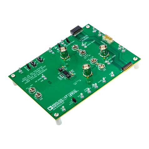
Analog Devices LT7182S Quick setup guide

Analog Devices
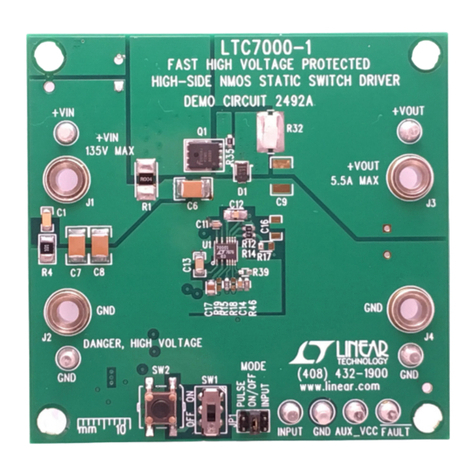
Analog Devices Linear DC2492A User manual

Analog Devices
Analog Devices EZ-KIT User manual

Analog Devices
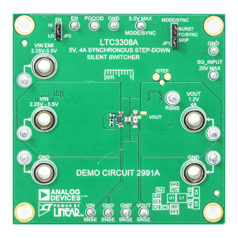
Analog Devices LTC3308A Quick setup guide

Analog Devices
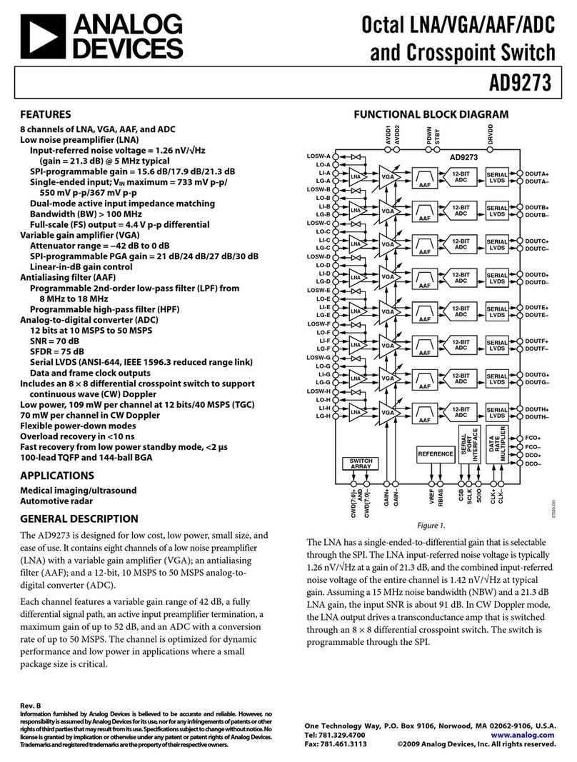
Analog Devices AD9273 User manual