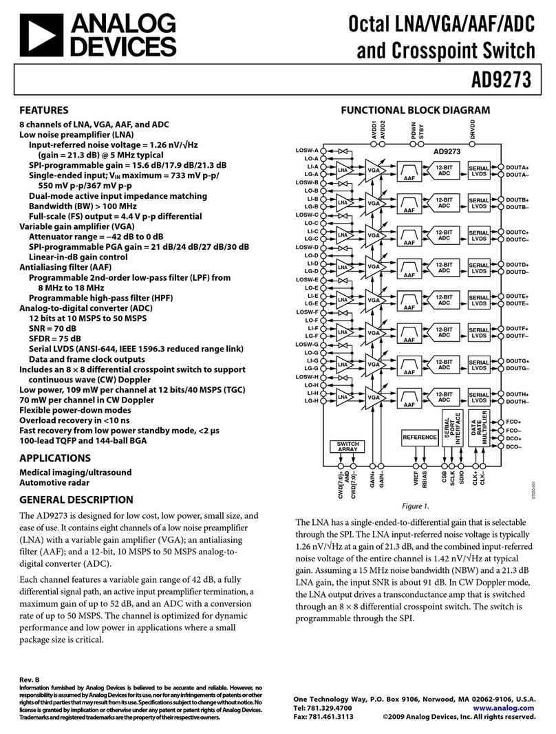
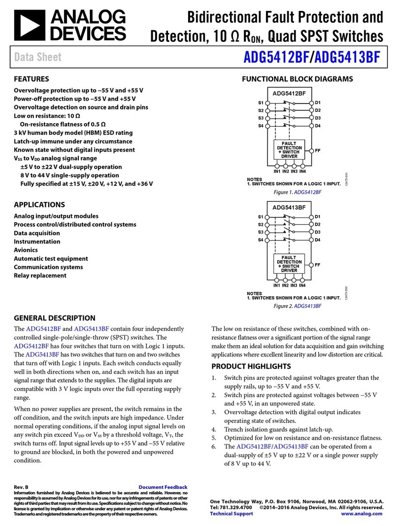
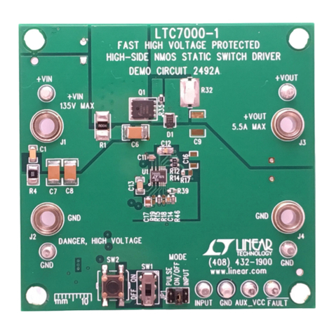
Analog Devices LINEAR LTM 8005 User manual

LTM8005
1
Rev. B
For more information www.analog.comDocument Feedback
TYPICAL APPLICATION
FEATURES DESCRIPTION
38VIN Boost µModule Regulator for
LED Drive with 10A Switch
The LT M
®
8005 is a 38VIN, 38VOUT boost µModule (power
micromodule) LED driver designed to regulate current or
voltage and is ideal for driving LEDs. The fixed frequency
and current mode architecture result in stable operation
over a wide range of supply and output voltages. Spread
spectrum frequency modulation (SSFM) can be activated
for improved electromagnetic compatibility (EMC) perfor-
mance. The ground-referred voltage FB pin serves as the
input for several LED protection features, and also allows the
converter to operate as a constant voltage source. The PWM
input provides LED dimming ratios of up to 3000:1, and the
CTRL inputs provide additional analog dimming capability.
The low profile package enables utilization of unused
space on the bottom of PC boards. The LTM8005 is pack-
aged in thermally enhanced, compact over-molded Ball
Grid Array (BGA) package suitable for automated assem-
bly by standard surface mount equipment. The LTM8005
is RoHS compliant.
350mA at 30.5V to 35.5V LED String from 6V to 27V VIN (Boost) with Spread Spectrum
APPLICATIONS
n Wide Input Voltage Range: 5V to 38V
n Supports Boost or SEPIC Power Topologies
n Adjustable LED Current Up to 1.6A
n 40V 10A Internal Power Switch
n Wide Temperature Range: –40°C to 150°C
n Input and Output Current Reporting
n Internal Switch for PWM and Output Disconnect
n Internal Spread Spectrum Frequency Modulation
n 3000:1 True Color PWM™ Dimming
n Open LED Protection with OPENLED Flag
n Short-Circuit Protection and SHORTLED Flag
n Soft-Start with Programmable Fault Restart Timer
n 9mm × 11.25mm × 2.22mm BGA
n High Power LED, High Voltage LED
n Accurate Current-Limited Voltage Regulators
All registered trademarks and trademarks are the property of their respective owners.
LTM8005
8005 TA01a
EN/UVLO
OVLO
PWM
VREF
CTRL1
CTRL2
VOUT
ISN
LED
AUX
FB
ISMON
RAMPSS VC RT GND OPENLED SHORTLED
IVINPVIN IVINN SW DA
LED
STRING
COUT
2×
4.7µF
50V
L
8.2µH
L: COILCRAFT XAL7030-822ME
CIN, COUT: MURATA GRM31CR71H475KA12
PIN NOT USED IN THIS CIRCUIT: IVINCOMP
100k
93.1k
1M
19.1k
4.7k 23.2k
f = 350kHz
10nF
6.8nF
0.1µF
0.1µF
CIN
2×
4.7µF
50V
12.4k
374k
VIN
6V TO 27V
18.7k

LTM8005
2
Rev. B
For more information www.analog.com
PIN CONFIGURATION
ABSOLUTE MAXIMUM RATINGS
VIN, EN/UVLO, IVINN, IVINP .....................................50V
ISN Above LED..........................................................40V
SW, ISN, LED, VOUT, VOUT-DA..................................40V
CTRL1, CTRL2 ………………...................................15V
PWM, SHORTLED, OPENLED ...................................12V
FB, OVLO ....................................................................8V
Maximum Junction Temperature
(E-Grade, I-Grade) ............................................ 125°C
Maximum Junction Temperature (H-Grade).......... 150°C
Storage Temperature............................................. 150°C
Peak Solder Reflow Body Temperature ................. 260°C
(Note 1)
FG H JK
E
ABCD
2
1
4
3
5
6
7
8
BGA PACKAGE
80-Pad (11.25mm ×9mm ×2.22mm)
θ
JA
= 19.3°C/W,
θ
JCBOTTOM
= 3.0°C/W,
θJCTOP = 16.3°C/W, θJB = 7.2°C/W, WEIGHT = 0.4g
θVALUES DETERMINED PER JEDEC 15-9, 51-12
TOP VIEW
GND
CTRL2
CTRL1
RT
SS
VC
FB
GND
BANK 5
ISN
IVINN
VIN
BANK 2
SW
BANK 1
GND
IVINP
EN/UVLO
IVINCOMP
AUX
ISMON
BANK 6
LED
BANK 4 VOUT
BANK 3 DA
OPENLED
SHORTLED
RAMP
PWM
VREF
OVLO
ORDER INFORMATION
Part Number Terminal Finish Part Marking* Package Type MSL Rating Temperature Range
Device Finish Code
LTM8005EY#PBF SAC305 (RoHS) LTM8005 e1 BGA 3 –40°C to 125°C
LTM8005IY#PBF SAC305 (RoHS) LTM8005 e1 BGA 3 –40°C to 125°C
LTM8005HY#PBF SAC305 (RoHS) LTM8005 e1 BGA 3 –40°C to 150°C
Contact the factory for parts specified with wider operating temperature
ranges. *Device temperature grade is identified by a label on the shipping
container. Pad or ball finish code is per IPC/JEDEC J-STD-609.
• Recommended LGA and BGA PCB Assembly and Manufacturing
Procedures
• LGA and BGA Package and Tray Drawings

LTM8005
3
Rev. B
For more information www.analog.com
ELECTRICAL CHARACTERISTICS
PARAMETER CONDITIONS MIN TYP MAX UNITS
Minimum Input Voltage l5 V
LED DC Current CTRL1=1.5V
CTRL1=0.6V
CTRL1=0.2V
1.65
0.8
0.16
A
A
A
SW Current Limit 10 12 14 A
SW RDS(ON) 19 mΩ
ISMON Voltage ILED=1.5A 0.88 0.96 V
Quiescent Current into VIN EN/UVLO=0V (Disabled), PWM=0V
EN/UVLO=1.15V, PWM=0V
RT=82.5K to GND, FB=1.5V (Not Switching)
35
40
3.5
µA
µA
mA
VREF Voltage IREF=–100µA l1.95 2.00 2.08 V
VREF Line Regulation 5V < VIN < 48V 0.1 %
VREF Load Regulation –100µA < IREF < 0µA 1 %
SS Current Sourcing, SS=0V
Sinking, ILED Overcurrent
28
2.8
µA
µA
ILED Overcurrent Threshold 2.4 A
ISN-LED RDS(ON) 53 mΩ
VC Output Impedance 2000 kΩ
VC Standby Input Bias Current PWM=0V –20 20 nA
VC Pin Current VC=1.2V, Sourcing
VC=1.2V, Sinking
10
30
µA
µA
Voltage at FB pin l1.23 1.25 1.27 V
FB Amplifier gm500 µS
FB Pin Input Bias Current Current Out of Pin, FB=VFB 200 nA
FB OPENLED Threshold OPENLED Falling 1.176 1.222 V
FB Overvoltage Threshold 1.26 1.34 V
FB SHORTLED Threshold SHORTLED Falling 300 350 mV
LED Current C/10 Threshold 0.16 A
Input Current Limit Threshold IVINP–IVINN 53 67 mV
IVINCOMP Voltage IVINP–IVINN=60mV 1.2 V
Switching Frequency RT=82.5k
RT=26.1k
RT=6.65k
85
240
800
105
300
1000
125
360
1200
kHz
kHz
kHz
Switching Frequency Modulation RAMP=2V 70 %
RAMP Input Low Threshold 1 V
RAMP Input High Threshold 2 V
RAMP Pin Source Current RAMP=0.4V 12 µA
RAMP Pin Sink Current RAMP=1.6V 12 µA
CTRL1, CTRL2 Pin Current CTRL1, CTRL2=1V 200 nA
PWM Input Threshold Rising 1 V
PWM Pin Bias Current 10 µA
The ldenotes the specifications which apply over the specified operating
temperature range, otherwise specifications are at TA= 25°C. CTRL1=CTRL2=PWM=5V, unless otherwise noted (Note 2).

LTM8005
4
Rev. B
For more information www.analog.com
ELECTRICAL CHARACTERISTICS
PARAMETER CONDITIONS MIN TYP MAX UNITS
EN/UVLO Threshold Voltage Falling 1.22 V
EN/UVLO Threshold Voltage Rising 1.24 V
EN/UVLO Pin Bias Current EN/UVLO=1.15V, VIN = 12V 19 µA
OPENLED Output Low IOPENLED=0.5mA 0.3 V
SHORTLED Output Low ISHORTLED=0.5mA 0.3 V
OVLO Threshold Voltage Rising
Falling
1.21
1.17
1.30
1.26
V
V
The ldenotes the specifications which apply over the specified operating
temperature range, otherwise specifications are at TA= 25°C. CTRL1=CTRL2=PWM=5V, unless otherwise noted (Note 2).
Note 1: Stresses beyond those listed under Absolute Maximum Ratings
may cause permanent damage to the device. Exposure to any Absolute
Maximum Rating condition for extended periods may affect device
reliability and lifetime.
Note 2: The LTM8005E is guaranteed to meet performance specifications
from 0°C to 125°C internal. Specifications over the full –40°C to
125°C internal operating temperature range are assured by design,
characterization and correlation with statistical process controls. The
LTM8005I is guaranteed to meet specifications over the full –40°C
to 125°C internal operating temperature range. The LTM8005MP is
guaranteed to meet specifications over the full –55°C to 125°C internal
operating temperature range. The LTM8005H is guaranteed to meet
specifications over the full –40°C to 150°C internal operating temperature
range. Note that the maximum internal temperature is determined by
specific operating conditions in conjunction with board layout, the rated
package thermal resistance and other environmental factors.
Note 3: The LTM8005 contains over-temperature protection that is
intended to protect the device during momentary overload conditions. The
internal temperature exceeds the maximum operating junction temperature
when the over-temperature protection is active. Continuous operation
above the specified maximum operating junction temperature may impair
device reliability.

LTM8005
5
Rev. B
For more information www.analog.com
TYPICAL PERFORMANCE CHARACTERISTICS
VREF vs Load
Switching Frequency
vs SS Voltage
Demonstration Circuit DC2257A
Output Current Ripple 34V at 1.2A
LED, 12VIN
DC2257A Conducted EMI with and
without Spread Spectrum Enabled
LED Current vs CTRL1 LED Current vs CTRL2
LED Current vs FB
(CTRL1=CTRL2=VREF)
TA= 25°C, unless otherwise noted.
CTRL1 VOLTAGE (V)
0
0.25
0.50
0.75
1
1.25
1.50
0
0.4
0.8
1.2
1.6
2.0
LED CURRENT (A)
8005 G01
CTRL2 VOLTAGE (V)
0
0.25
0.50
0.75
1
1.25
1.50
0
0.4
0.8
1.2
1.6
2.0
LED CURRENT (A)
8005 G02
V
FB
(V)
0
0.3
0.6
0.9
1.2
1.5
0
0.5
1.0
1.5
2.0
LED CURRENT (A)
8005 G03
VREF vs Load Current
LOAD CURRENT (µA)
0
45
90
135
180
0
0.5
1.0
1.5
2.0
2.5
VREF (V)
8005 G04
V
SS
(V)
0
0.3
0.6
0.9
1.2
1.5
RT= 23.2k
0
70
140
210
280
350
FREQUENCY (kHz)
8005 G05
1µs/DIV
CURRENT RIPPLE
50mA/DIV
8005 G06
C
RAMP
= 22nF
SPREAD SPECTRUM DISABLED
SPREAD SPECTRUM ENABLED
FREQUENCY (MHz)
0.1
1.1
2.1
3.0
4.0
5.0
1
21
41
60
80
100
EMISSIONS (dBµV)
8005 G07

LTM8005
6
Rev. B
For more information www.analog.com
TYPICAL PERFORMANCE CHARACTERISTICS
Output Disconnect Response
(Short Circuit)
Output Disconnect Response
(Input > Output)
DC2257A CISPR 22 Radiated
Results Without Spread Spectrum
DC2257A CISPR 22 Radiated
Results With Spread Spectrum
TA= 25°C, unless otherwise noted.
500ns/DIV
VOUT
10V/DIV
VLED
10V/DIV
ILED
10A/DIV
8005 G10
1ms/DIV
VIN
10V/DIV
VOUT
10V/DIV
VLED
10V/DIV
8005 G11
SPREAD SPECTRUM DISABLED
FREQUENCY (MHz)
0
250
500
750
1000
0
10
20
30
40
EMISSIONS (dBµV/m)
8005 G08
SPREAD SPECTRUM ENABLED
FREQUENCY (MHz)
0
250
500
750
1000
0
10
20
30
40
EMISSIONS (dBµV/m)
8005 G09

LTM8005
7
Rev. B
For more information www.analog.com
PIN FUNCTIONS
GND (Bank 1, Pin K1, Pin K8): Tie these GND pins to a
local ground plane below the LTM8005 and the circuit
components. In most applications, the bulk of the heat
flow out of the LTM8005 is through these pads, so the
printed circuit design has a large impact on the thermal
performance of the part. See the PCB Layout and Thermal
Considerations sections for more details. Return the feed-
back divider to this net.
SW (Bank 2):Power Switch Node. This is the drain of the
internal power switching MOSFET. For boost, buck-boost
mode and buck mode topologies, connect this bank to
the inductor and the DA bank. For a SEPIC, connect this
bank to an inductor winding and the positive coupling
capacitor terminal.
DA (Bank 3):Power Diode Anode. For boost, buck-boost
mode and buck mode topologies, connect this bank to
the inductor and the SW bank. For a SEPIC, connect this
bank to an inductor winding and the negative coupling
capacitor terminal.
VOUT (Bank 4):Power Output Pins. Apply the output filter
capacitor between these pins and the GND pins.
ISN (Bank 5):Output Current Sense Resistor. The
LTM8005 incorporates a sense resistor between VOUT
and ISN to set the output current regulation point and
for output current monitoring. If a larger output current
is required, apply an external resistor between VOUT and
ISN. Keep this pin voltage within 0.3V of VOUT.
LED (Bank 6):LED Current Output. Connect the anode of
the LED string to this bank.
VIN (Pin F1): Input Power. The VIN pin supplies current to
the LTM8005’s internal regulators and circuitry, and must
be bypassed with a 0.22µF (or larger) capacitor placed
close to the LTM8005.
IVINN (Pin F2): Input Sense Resistor Signal. Apply an
external sense resistor between IVINP and IVINN to set
the maximum input current and for input current moni-
toring. If this function is not required, tie both IVINP and
IVINN to VIN. Keep this pin voltage within 0.3V of VIN.
EN/UVLO (Pin G1): Enable and Precision UVLO. An accu-
rate 1.22V falling threshold with externally programmable
hysteresis detects when power is OK to enable switching.
Rising hysteresis is generated by the external resistor
divider, an internal 499kΩ resistor between EN/UVLO and
VIN and an accurate internal 3µA pull-down current. Above
the threshold, EN/UVLO input bias current is sub-µA.
Below the falling threshold, a 3µA pull-down current is
enabled so the user can optimize the hysteresis with the
external resistor selection. An undervoltage condition
resets soft-start. The EN/UVLO pin may be connected
directly to VIN, but do not drive this pin directly from
another low impedance voltage source. If EN/UVLO must
be driven from a voltage source, do so with at least a 50Ω
series resistor.
IVINP (Pin G2): Input Sense Resistor Signal. Apply an
external sense resistor between IVINP and IVINN to set
the maximum input current and for input current moni-
toring. If this function is not required, tie both IVINP and
IVINN to VIN. Keep this pin voltage within 0.3V of VIN.
OVLO (Pin H1): Input Overvoltage Lockout Pin. An
accurate 1.25V rising threshold detects when power is
OK to enable switching. If not used, tie this pin to GND.
IVINCOMP (Pin H2): Input Current Sense Amplifier Output
Pin. The voltage at IVINCOMP pin is proportional to IIN as
VIVINCOMP = IIN • RINSNS • 20. A 10nF capacitor to GND
is provided internally at this pin to compensate the input
current loop. Do not load this pin with a current and do not
drive this pin with an external source, although additional
capacitance may be added externally.
SHORTLED (Pin H7): An open-collector pull-down on
SHORTLED asserts when any of the following conditions
happen:
1. FB < 0.3V after SS pin reaches 1.7V at start-up.
2. LED overcurrent (ILED > 2.4A).
To function, the pin requires an external pull-up resistor.
SHORTLED status is only updated during PWM high state
and latched during PWM low state. SHORTLED remains
asserted until the SS pin is discharged below 0.2V. If not
used, leave floating or tie to GND.
OPENLED (Pin H8): Fault Indicator. An open-collector
pull-down on OPENLED asserts if the FB input is above
1.20V (typical), and the LED current is less than 0.16A
(typical). To function, the pin requires an external pull-up

LTM8005
8
Rev. B
For more information www.analog.com
resistor. OPENLED status is updated only during PWM
high state and latched during PWM low state. If not used,
leave floating or tie to GND.
ISMON (Pin J1): LED Current Report Pin. The LED cur-
rent is reported as VISMON = (LED current)/1.6. Leave the
ISMON pin unconnected if not used. When PWM is low,
ISMON is driven to ground. Bypass with a 47nF capacitor
or higher if needed. Do not drive this pin with an external
source.
AUX (Pin J2): Auxiliary Pin. This pin is internally con-
nected to VOUT to ease layout. Conveniently located next
to FB, it is provided to simplify layout of the output voltage
feedback network.
VREF (Pin J6): Voltage Reference Output Pin. Typically 2V.
This pin drives a resistor divider for the CTRL pins, either
for analog dimming or for temperature limit/compensa-
tion of the LED load. It can supply up to 100µA. Do not
drive this pin with an external source.
PWM (Pin J7): PWM Input Signal Pin. A low signal turns
off switching, idles the oscillator, disconnects the VC pin
from all internal loads, and disconnects the output load
from VOUT. PWM has an internal 500kΩ pull-down resis-
tor. If not used, connect to VREF.
RAMP (Pin J8): The RAMP pin is used for spread spec-
trum frequency modulation. The internal switching fre-
quency is spread out to 70% of the original value, where
the modulation frequency is set by 12µA/(2 • 1V • CRAMP).
If not used, tie this pin to GND.
FB (Pin K2): Voltage Loop Feedback Pin. FB is intended
for constant-voltage regulation or for LED protection/open
LED detection. The internal transconductance amplifier
with output VC regulates FB to 1.25V (nominal) through
the DC/DC converter. If the FB input is regulating the loop,
and LED current is less than 0.15A (typical), the OPENLED
pull-down is asserted. This action may signal an open LED
fault. If FB is driven above 1.3V (by an external power sup-
ply spike, for example), the internal N-Channel MOSFET
is turned off and the load is disconnected from VOUT to
protect the LEDs from an overcurrent event. Do not tie
this pin to GND as the SHORTLED will be asserted and
the part will be shut down.
VC (Pin K3): Transconductance Error Amplifier Output Pin.
Used to stabilize the control loop with an RC network. This
pin is high impedance when PWM is low, a feature that
stores the demanded current state variable for the next
PWM high transition. Connect a capacitor between this pin
and GND;a resistor in series with the capacitor is recom-
mended for fast transient response. Do not leave this pin
open, and do not drive this pin with an external source.
SS (Pin K4): Soft-Start Pin. This pin modulates oscillator
frequency and compensation pin voltage (VC). The soft-
start interval is set with an external capacitor. The pin
has a 28µA (typical) pull-up current source to an internal
2.5V rail. This pin can be used as fault timer. Provided the
SS pin has exceeded 1.7V to complete a blanking period
at start-up, the pull-up current source is disabled and a
2.8µA pull-down current is enabled when any one of the
following fault conditions happen:
1. LED overcurrent (ILED > 2.4A)
2. Output short (FB < 0.3V after start-up)
3. Thermal limit
The SS pin must be discharged below 0.2V to re-initiate
a soft-start cycle. Switching is disabled until SS begins to
recharge. It is important to select a capacitor large enough
that FB can exceed 0.3V under normal load conditions
before SS exceeds 1.7V. Do not leave this pin open and
do not drive this pin with an external source.
RT (Pin K5): Switching Frequency Adjustment Pin. Set
the frequency using a resistor to GND. Do not leave the
RT pin open. Do not drive this pin with an external source.
CTRL1, CTRL2 (Pin K6, K7): Current Sense Threshold
Adjustment. CTRL1 and CTRL2 have identical functions.
The output current is regulated by CTRL1 or CTRL2.
The pin with the lowest voltage takes precedence. For
0.1V<VCTRLx<1V the LED current is VCTRLx• 1.5A
less an offset. For VCTRLx > 1.2V the current sense
threshold is constant at the full-scale value of 1.6A. For
1V<VCTRLx<1.2V, the dependence of the current sense
threshold upon VCTRLx transitions from a linear function
to a constant value, reaching 98% of full-scale value by
VCTRLx = 1.1V. Do not leave this pin open. If not used, tie
to VREF. Connect either CTRL pin to GND for zero LED
current.
PIN FUNCTIONS
LTM8005
10
Rev. B
For more information www.analog.com
OPERATION
The LTM8005 is a stand-alone non-isolated switching DC/
DC regulator intended for LED driver applications. This
µModule power converter provides a regulated current
from an input voltage range of 5V to 38V, and up to 38V
output. A simplified block diagram is provided in the pre-
vious section.
The LTM8005 is equipped with a ground referred power
switch and a power rectifier. Connect external power
devices, such as an inductor, to these pins to implement
boost, buck-boost mode, buck mode or SEPIC topologies
to drive a string of LEDs.
The LTM8005 features an integrated sense resistor to
control the LED current. The maximum regulated current
is 1.6A, and this can be reduced by applying a voltage less
than 1.2V to the CTRL1 or CTRL2 pins. The output current
is reported by the voltage on the ISMON pin.
The LTM8005 also features an integrated PMOS discon-
nect switch to implement PWM dimming that is controlled
by a signal on the PWM pin. The PMOS also disconnects
the LEDs during fault conditions.
If input current limiting is desired, apply an external sense
resistor to the IVINP and IVINN pins. The full input current
will flow through this external sense resistor, so choose a
resistor with an appropriate power rating. The LTM8005
will start to decrease the power if the voltage between the
IVINP and INVINN pins exceeds 60mV. A 10nF capacitor
is provided internally to compensate the input current
regulation loop, but additional capacitance may be added
externally to further filter the voltage at the IVINCOMP pin.
The LTM8005 features spread spectrum frequency
modulation, which causes the switching frequency to
modulate to a frequency that is approximately 70% of
the programmed value set by the RT resistor. This modu-
lation decreases the energy emitted at a single frequency,
reducing the EMI amplitude. The modulation behavior is
set by a capacitor on the RAMP pin to GND.
Input voltage turn-on and turn-off thresholds are set
by resistor networks at the EN/UVLO and OVLO pins.
Applying a voltage of greater than 1.24V to the EN/UVLO
pin enables the part.
OPENLED and SHORTLED are active low open drain sta-
tus bits that indicate an open LED or shorted LED condi-
tion. OPENLED transitions to a logic low when the FB pin
rises above 1.2V and the LED current decreases below
160mA. SHORTLED transitions to a logic low when the FB
pin falls below 300mV or the LED current exceeds 2.4A.
Further details on these and other functions are given in
the Applications Information section.
An external soft start capacitor at the SS pin minimizes
the current spike that occurs at start up and the SS pin
also programs hiccup or latchoff mode fault protection.
The LTM8005 is equipped with a thermal shutdown that
inhibits power switching at high junction temperatures.
The activation threshold of this function is above the abso-
lute maximum temperature rating to avoid interfering with
normal operation, so prolonged or repetitive operation
under a condition in which the thermal shutdown activates
may damage or impair the reliability of the device.

LTM8005
11
Rev. B
For more information www.analog.com
Programming the Turn-On and Turn-Off Thresholds
with the EN/UVLO Pin
The falling under-voltage lockout (UVLO) value can be
accurately set by the resistor divider, as shown in Figure1.
A small 3µA pull-down current is active when EN/UVLO
is below the threshold. The purpose of this current is to
allow the user to program the rising hysteresis. The fol-
lowing equations should be used to determine the values
of the resistors:
VIN(FALLING) =1.22 •
R1499k
+
R2
R2
VIN(RISING) = VIN(FALLING) + (3µA • R1
!
499k)
LTM8005
8005 F01
VIN
VIN
EN/UVLO
R1
499k
R2
Figure1. Set an Accurate UVLO with a Resistor Divider
Programming the Overvoltage Lockout Threshold with
the OVLO Pin
The input overvoltage lockout protection feature can be
implemented by a resistor from the VIN to OVLO pins as
shown in Figure2. The following equations should be
used to determine the values of the resistors:
VIN,OVLO =1.25 •
R3
+
R4
R4
LTM8005
OVLO
VIN
R3
R4
8005 F02
Figure2. Set an Overvoltage Lockout Threshold with
a Resistive Divider
APPLICATIONS INFORMATION
LED Current Adjustment
The maximum output LED current is internally set to 1.6A,
typical. If both CTRL pins are tied to a voltage higher than
1.2V, maximum current is available. If a voltage less than
1.2V is applied to either CTRL1 or CTRL2, the LED current
will decrease. The two CTRL pins have identical func-
tions. Whichever is the lowest takes precedence. Either
CTRL pin can also be used to dim the LED current to zero,
although relative accuracy decreases with the decreasing
applied voltage sense threshold.
The CTRL pins should not be left open (tie to VREF if not
used). Either CTRL pin can also be used in conjunction
with a thermistor to provide overtemperature protection
for the LED load, or with a resistor divider to VIN to reduce
output power and switching current when VIN is low.
Internal Power Switch Voltage Stress
The LTM8005 is equipped with an integrated ground
referred N-channel power MOSFET whose drain is con-
nected to the SW bank. The absolute maximum rating
of the SW bank is 40V. When using the LTM8005 in a
boost power topology, the voltage stress on the SW bank
is nominally a diode drop above VOUT. In the SEPIC or
buck-boost topologies, however, the voltage stress on the
SW bank is substantially higher than VOUT, nominally VIN
+ VOUT. Do not exceed the absolute maximum voltage of
the SW bank under any operating condition.
Programming Output Voltage (Constant-Voltage
Regulation) and Output Voltage Open LED and
Shorted LED Thresholds
The LTM8005 has a voltage feedback pin FB that can be
used to program a constant-voltage output. In addition,
FB programming determines the output voltage that will
cause OPENLED and SHORTLED to assert. For a boost

LTM8005
12
Rev. B
For more information www.analog.com
APPLICATIONS INFORMATION
LED driver, the output voltage can be programmed by
selecting the values of R5 and R6 (see Figure3) according
to the following equation:
VOUT =1.25 •
R5
+
R6
R6
LTM8005
FB
VOUT
R5
R6
8005 F03
Figure3. Set the OPENLED and SHORTLED Voltage
Thresholds with Two Resistors
For a LED driver in buck-boost mode or buck mode con-
figuration, the FB voltage is typically level shifted to a
signal with respect to GND as illustrated in Figure4. The
output can be expressed as:
VOUT =1.25 • R7
R8
+VBE(Q1)
LTM8005
FB
R7
Q1
RSENSE
R8
8005 F04
LED
ARRAY
VOUT
+
–
Figure4. Level Shifting the FB Voltage is Commonly
Used in Buck-Boost Mode or Buck Mode Configurations
If the open LED clamp voltage is programmed correctly
using the resistor divider, then the FB pin should never
exceed 1.2V when LEDs are connected. To detect both
open-circuit and short-circuit conditions at the output,
the LTM8005 monitors both output voltage and current.
When FB exceeds 1.2V, OPENLED is asserted if the out-
put current is less than about 160mA. OPENLED is de-
asserted when the output current increases above about
0.45A or FB drops below 1.19V (typical). The SHORTLED
pin is asserted if the output current is about 2.4A or the FB
pin falls below 300mV (typical) after initial start-up and SS
reaches about 1.7V. The ratio between the FB OPENLED
threshold of 1.2V and the SHORTLED threshold of 0.3V
can limit the range of VOUT. The range of VOUT using the
maximum SHORTLED threshold of 0.35V is about 3.5:1.
The range of VOUT can be made wider using the circuits
shown in Figure5 and Figure6. For a VOUT range that is
greater than 8:1, consult factory applications.
LTM8005
FB
VOUT
VREF
R10
R12
R11
8005 F05
Figure5. Feedback Resistor Connection for Wide Range
Output in Boost and SEPIC Applications
VREF
R15
LTM8005
FB
R13
Q1
RSENSE
R14
8005 F06
LED
ARRAY
VOUT
+
–
Figure6. Feedback Resistor Connection for Wide Range
Output in Buck-Boost Mode or Buck Mode Applications
The equations to widen the range of VOUT are derived
using a SHORTLED threshold of 0.35V, an OPENLED
threshold of 1.2V and a reference voltage VREF of 2V.
The resistor values for R11 and R12 in Figure5 can be
calculated as shown below. See the example that follows
for a suggested R10 value.
R11=1.7 • R10
1.65 • V
OUTMAX
( )
– 0.8 • V
OUTMIN
( )
– 1.7
R12 =
1.7 • R10
0.35 • VOUTMAX
( )
– 1.2 • VOUTMIN
( )

LTM8005
13
Rev. B
For more information www.analog.com
APPLICATIONS INFORMATION
Example:Calculate the resistor values required to increase
the VOUT range of a boost LED driver to 7.5:1 and have
OPENLED occur when VOUT is 38V:
Step 1: Choose R10 = 374k
Step 2: VOUTMIN = 38/7.5 = 5.1
Step 3:
R11=
1.7 • 374k
Ω
1.65 • 38
( )
– 0.8 • 5.1
( )
– 1.7 =11.2kΩ
Use R11 = 11.3kΩ.
R12 =
1.7 • 374k
Ω
0.35 • 38
( )
– 1.2 • 5.1
( )
=88.6kΩ
Use R12 = 88.7K.
The resistor values for R14 and R15 in Figure6 can be
calculated as shown below. See the example that follows
for a suggested R13 value.
R14 =1.7 • R13
1.65 • VOUTMAX
( )
– 0.8 • VOUTMIN
( )
– 0.85 • VBE(Q1)
( )
R15 =1.7 • R13
0.35 • VOUTMAX
( )
– 1.2 • VOUTMIN
( )
– 0.85 • VBE(Q1)
( )
Example:Calculate the resistor values required to increase
the VOUT range of a buck-boost mode LED driver to
5:1 and have OPENLED occur when VOUT is 17V. Use
VBE(Q1)=0.7V:
Step 1: Choose R13 = 187k
Step 2: VOUTMIN = 17/5 = 3.4
Step 3:
R14 =
1.7 • 187k
Ω
1.65 • 17
( )
– 0.8 • 3.4
( )
– 0.85 • 0.7
( )
=12.9kΩ
Use R14 = 12.7kΩ
R15 =1.7 • 187kΩ
0.35 • 17
( )
– 1.2 • 3.4
( )
– 0.85 • 0.7
( )
=249kΩ
Use R15 = 249kΩ
LED Overcurrent Protection Feature
The LTM8005 has an overload protection feature inde-
pendent of the output LED current regulation. This feature
prevents the development of excessive switching currents
and protects the power components. The overload protec
-
tion threshold (2.4A typical) is designed to be 50% higher
than the default LED current sense threshold. Once the
LED overcurrent is detected, the internal power switch is
turned off to stop switching, the PWM MOSFET is turned
off to disconnect the LED array from the power path, and
fault protection is initiated via the SS pin.
An anti-parallel Schottky or ultrafast diode D2 should be
connected as shown in Figure7 to protect the LED node
from swinging well below ground when being shorted to
ground through a long cable. The internal protection loop
takes a finite amount of time to respond to the overload,
so the diode is recommended if the system must survive
an overload on the LED string.
LTM8005
LED
GND
D2
8005 F07
LED
STRING
PARASITIC
INDUCTANCE OF
LONG CABLE
Figure7. Connect an Anti-Parallel Diode D2 from
LED to GND to Protect the LTM8005 from Negative
Voltage Swings when the Connecting to a LED
String through a Long Cable

LTM8005
14
Rev. B
For more information www.analog.com
APPLICATIONS INFORMATION
PWM Dimming Control for Brightness
There are two methods to control the LED current for
dimming using the LTM8005. One method uses the CTRL
pins to adjust the current regulated in the LEDs. A sec-
ond method uses the PWM pin to modulate the LED cur-
rent between zero and full current to achieve a precisely
programmed average current, without the possibility of
color shift that occurs at low current in LEDs. To make
PWM dimming more accurate, the switch demand cur-
rent is stored on the VC node during the quiescent phase
when PWM is low. This feature minimizes recovery time
when the PWM signal goes high. To further improve the
recovery time, a disconnect MOSFET switch has been
implemented to open the LED current path to prevent the
output capacitor from discharging during the PWM signal
low phase. The minimum PWM on or off time depends
on the choice of operating frequency set by the RT input.
For best current accuracy, the minimum recommended
PWM high time should be at least three switching cycles
(3µs for fSW = 1MHz).
A low duty cycle PWM signal can cause excessive start-up
times if it is allowed to interrupt the soft-start sequence.
Therefore, once start-up is initiated by a PWM signal, the
LTM8005 will ignore a logical disable by the external PWM
input signal. The device will continue to soft-start with
switching and TG enabled until either the voltage at SS
reaches about 1V or the output current reaches one-fourth
of the full-scale current. At this point the device will begin
following the dimming control as designated by PWM. If
at any time an output overcurrent is detected, the internal
MOSFETs will be disabled even as SS continues to charge.
Programming the Switching Frequency
The RT frequency adjust pin allows the user to program
the switching frequency from 100kHz to 1MHz to opti-
mize efficiency/performance or external component size.
Higher frequency operation yields smaller component
size but increases switching losses and gate driving cur-
rent, and may not allow sufficiently high or low duty cycle
operation. Lower frequency operation gives better perfor-
mance at the cost of larger external component size. For
an appropriate RT resistor value see Table1. An external
resistor from the RT pin to GND is required—do not leave
this pin open.
Table1. Typical Switching Frequency vs RTValue (1% Resistor)
fOSC(kHz) RT(kΩ)
1000 6.65
900 7.50
800 8.87
700 10.2
600 12.4
500 15.4
400 19.6
300 26.1
200 39.2
100 82.5
Spread Spectrum Frequency Modulation
Switching regulators can be particularly troublesome
for applications where electromagnetic interference
(EMI) is a concern. To improve the EMI performance,
the LTM8005 includes a spread spectrum frequency fea-
ture. If there is a capacitor (CRAMP) at the RAMP pin, a
triangle wave sweeping between about 1V and 2V is gen-
erated. This signal is then fed into the internal oscillator
to modulate the switching frequency between about 70%
of the base frequency and the base frequency, which is
set by the RT resistor. The modulation frequency is set by
12µA/(2 • 1V • CRAMP). The results of EMI measurements
are sensitive to the RAMP frequency selected with the
capacitor. 1kHz is a good starting point to optimize peak
measurements, but some fine tuning of this selection
may be necessary to get the best overall EMI results in a
particular system. Consult factory applications for more
detailed information about EMI reduction. The Typical
Performance Characteristics section contains plots that
show the LTM8005 conducted and radiated emissions
with and without Spread Spectrum enabled.

LTM8005
15
Rev. B
For more information www.analog.com
APPLICATIONS INFORMATION
Duty Cycle Considerations
Switching duty cycle is a key variable defining converter
operation; therefore, its limits must be considered when
programming the switching frequency for a particular
application. The fixed minimum on-time and minimum
off-time and the switching frequency define the minimum
and maximum duty cycle of the switch, respectively. When
calculating operating limits, use typical room temperature
values of 320ns and 290ns for minimum on-time and
off-time, respectively.
Setting Input Current Limit
The LTM8005 has a standalone input current sense ampli-
fier to limit the input current. The input current I
IN
shown in
Figure8 is converted to a voltage output at the IVINCOMP
pin. When the IVINCOMP voltage exceeds 1.2V the inter-
nal power switch is turned off, and the converter stops
switching. The input current limit is calculated as follows:
IIN =
60mV
R
INSNS
the ISP/ISN regulation loop, which consists of the output
capacitance COUT and the dynamic resistance of the LED
load. The minimum CFILT value of 10nF is integrated into
the LTM8005.
Loop Compensation
The LTM8005 uses an internal transconductance error
amplifier whose VC output compensates the control loop.
The external inductor, output capacitor and the compen-
sation resistor and capacitor determine the loop stability.
The inductor and output capacitor are chosen based on
performance, size and cost. The compensation resistor
and capacitor at VC are selected to optimize control loop
response and stability. For typical LED applications, a
10nF compensation capacitor at VC is adequate, and a
series resistor should always be used to increase the slew
rate on the VC pin to maintain tighter regulation of LED
current during fast transients on the input supply to the
converter.
Soft-Start Capacitor Selection
For many applications, it is important to minimize the
inrush current at start-up. The LTM8005 soft-start cir-
cuit significantly reduces the start-up current spike and
output voltage overshoot. The soft-start interval is set by
the soft-start capacitor (CSS) selection according to the
equation:
TSS = CSS • 2V / 28µA
A typical value for the soft-start capacitor is 0.1µF. The
soft-start pin voltage reduces the oscillator frequency and
the maximum current in the switch. Soft-start also oper-
ates as fault protection, which forces the converter into
hiccup or latchoff mode. Detailed information is provided
in the Fault Protection:Hiccup Mode and Latchoff Mode
section.
Fault Protection: Hiccup Mode and Latchoff Mode
If an LED overcurrent condition, internal INTVCC under-
voltage, output short (FB ≤ 0.3V), or thermal limit hap-
pens, the integrated PMOS disconnect switch disconnects
the LED array from the power path, and the integrated
power switching MOSFET is turned off. If the soft-start
pin is charging and still below 1.7V, then it will continue
Figure8. Apply a Current Sense Resistor Between
IVINP and IVINN to Limit Input Current
Filter capacitor CFILT shown in Figure8 filters the voltage
at the IVINCOMP pin to minimize ripple due to the input
current. CFILT also compensates the input current regula-
tion loop, and is selected based on the loop response
in addition to the intended voltage ripple on IVINCOMP.
The IVINCOMP pin resistance to ground and CFILT form a
second pole in the input current regulation loop in addi-
tion to the dominant pole at VC pin. Suggested values for
CFILT of 10nF to 0.1µF will usually provide a second pole
in the input current regulation loop that results in stable
loop response and is equivalent to the second pole in
LTM8005
IVINP IVINN
IVINCOMP
8005 F08
TO LOAD
RINSNS
IIN
VIN
CFILT

LTM8005
16
Rev. B
For more information www.analog.com
APPLICATIONS INFORMATION
to do so with a 28µA source. Once above 1.7V, the pull-
up source is disabled and a discharge current of about
2.8µA is activated. While the SS pin is discharging, the
integrated switching MOSFET is turned off. When the
SS pin is discharged below about 0.2V, a new cycle is
initiated. This is hiccup mode operation. If the fault still
exists when SS crosses below about 0.2V, then a full SS
charge/discharge cycle has to complete before switching
is enabled.
If a resistor, typically 402kΩ, is placed between the VREF
pin and SS pin to hold SS pin higher than 0.2V during
a fault, then the LTM8005 will enter latchoff mode with
switching stopped and the load disconnected from VOUT.
To exit latchoff mode, the EN/UVLO pin must be toggled
low to high.
Capacitor Selection Considerations
Ceramic capacitors are small, robust and have very low
ESR. However, not all ceramic capacitors are suitable. X5R
and X7R types are stable over temperature and applied
voltage and give dependable service. Other types, includ-
ing Y5V and Z5U have very large temperature and voltage
coefficients of capacitance. In an application circuit they
may have only a small fraction of their nominal capaci-
tance resulting in much higher output voltage ripple than
expected.
Another precaution regarding ceramic capacitors con-
cerns the maximum input voltage rating of the LTM8005.
A ceramic input capacitor combined with trace or cable
inductance forms a high Q (under damped) tank circuit.
If the LTM8005 circuit is plugged into a live supply, the
input voltage can ring to twice its nominal value, possi-
bly exceeding the device’s rating. This situation is easily
avoided; see the Hot-Plugging Safely section.
Input Capacitor Selection
The input capacitor supplies the transient input current for
the power inductor of the converter and must be placed
and sized according to the transient current require-
ments. The switching frequency, output current and tol-
erable input voltage ripple are key inputs to estimating
the capacitor value. An X7R type ceramic capacitor is a
good choice because it has the least variation with tem-
perature and DC bias. Typically, boost and SEPIC con-
verters require a lower value capacitor than a buck mode
converter.
In the buck mode configuration, the input capacitor has
large pulsed currents due to the current returned through
the Schottky diode when the switch is off. It is important
to place the capacitor as close as possible to the Schottky
diode and to the GND return of the switch. It is also impor-
tant to consider the ripple current rating of the capacitor.
For best reliability, this capacitor should have low ESR and
ESL and have an adequate ripple current rating.
Output Capacitor Selection
The selection of the output capacitor depends on the load
and converter configuration, i.e., step-up or step-down
and the operating frequency. For LED applications, the
equivalent resistance of the LED is typically low and the
output filter capacitor should be sized to attenuate the cur-
rent ripple. Use of an X5R or X7R type ceramic capacitor
is recommended.
To achieve the same LED ripple current, the required fil-
ter capacitor is larger in the boost and buck-boost mode
applications than that in the buck mode applications.
Lower operating frequencies will require proportionately
higher capacitor values. The component values shown in
the data sheet applications are appropriate to drive the
specified LED string. The product of the output capacitor
and LED string impedance decides the second dominant
pole in the LED current regulation loop. It is prudent to
validate the power supply with the actual load (or loads).
Inductor Selection
The inductor used with the LTM8005 should have a satu-
ration current rating appropriate to the peak inductor cur-
rent under all expected operating conditions. Choose an
inductor value based on operating frequency to provide
a peak-to-peak inductor ripple current appropriate to the
12A (typical) switch current limit and duty cycle.

LTM8005
17
Rev. B
For more information www.analog.com
APPLICATIONS INFORMATION
PCB Layout
Most of the headaches associated with PCB layout have
been alleviated or even eliminated by the high level of
integration of the LTM8005. The LTM8005 is neverthe-
less a switching power supply, and care must be taken to
minimize EMI and ensure proper operation. Even with the
high level of integration, you may fail to achieve specified
operation with a haphazard or poor layout. See Figure 9
for the suggested layout of a boost topology application
and Figure 10 for the suggested layout of a buck-boost
mode topology application. Ensure that the grounding and
heat sinking are acceptable.
A few rules to keep in mind are:
1. Place the R
FB
, R
T
and V
C
components as close as
possible to their respective pins.
2. Place the CIN capacitors as close as possible to the
VIN and GND connection of the LTM8005.
3. Place the COUT capacitors as close as possible to the
VOUT and GND connection of the LTM8005.
4. Place the CIN and COUT capacitors such that their
ground currents flow directly adjacent to or under-
neath the LTM8005.
Figure9. Layout Showing Suggested External Components, GND Plane and Thermal Vias for a Boost Application
8005 F09
(OPTIONAL
DIODE)
CTRL2
CTRL1
RT
SS
VC
FB
GND
GND
GND/THERMAL VIAS
ISN
VIN
SW
IVINP
EN/UVLO
AUX
VOUT
CIN
COUT
OPENLED
SHORTLED
RAMP
PWM
VREF
IVINN
VIN OVLO
GND
TO LED
STRING
TO LED STRING
CATHODE (BOOST)
LED

LTM8005
18
Rev. B
For more information www.analog.com
8005 F10
CTRL2
CTRL1
RT
SS
VC
FB
GND
GND
GND
GND/THERMAL VIAS
ISN
VIN
SW
AUX
VOUT
CIN
CLED COUT
OPENLED
SHORTLED
RAMP
PWM
VREF
OVLO
GND
TO LED
STRING
TO LED STRING
CATHODE (BOOST)
GND
(OPTIONAL
DIODE)
IVINP
EN/UVLO
IVINN
VIN
LED
APPLICATIONS INFORMATION
Figure10. Layout Showing Suggested External Components, GND Plane and Thermal Vias for a Buck-Boost Mode Application
5. Connect all of the GND connections to as large a cop-
per pour or plane area as possible on the top layer.
Avoid breaking the ground connection between the
external components and the LTM8005.
6. Use vias to connect the GND copper area to the
board’s internal ground planes. Liberally distribute
these GND vias to provide both a good ground con-
nection and thermal path to the internal planes of the
printed circuit board. Pay attention to the location and
density of the thermal vias in Figures 9 and 10. The
LTM8005 can benefit from the heat sinking afforded
by vias that connect to internal GND planes at these
locations, due to their proximity to internal power
handling components. The optimum number of
thermal vias depends upon the printed circuit board
design. For example, a board might use very small
via holes. It should employ more thermal vias than a
board that uses larger holes.

LTM8005
19
Rev. B
For more information www.analog.com
APPLICATIONS INFORMATION
Hot-Plugging Safely
The small size, robustness and low impedance of ceramic
capacitors make them an attractive option for the input
bypass capacitor of the LTM8005. However, these capaci-
tors can cause problems if the LTM8005 is plugged into
a live supply (see Analog Devices Application Note 88
for a complete discussion). The low loss ceramic capaci-
tor combined with stray inductance in series with the
power source forms an underdamped tank circuit, and
the voltage at the VIN pin of the LTM8005 can ring to
more than twice the nominal input voltage, possibly
exceeding the LTM8005’s rating and damaging the part.
If the input supply is poorly controlled or the LTM8005 is
hot-plugged into an energized supply, the input network
should be designed to prevent this overshoot. This can
be accomplished by installing a small resistor in series
to VIN, but the most popular method of controlling input
voltage overshoot is to add an electrolytic bulk cap to the
VIN net. This capacitor’s relatively high equivalent series
resistance damps the circuit and eliminates the voltage
overshoot. The extra capacitor improves low frequency
ripple filtering and can slightly improve the efficiency of
the circuit, though it is likely to be the largest component
in the circuit.
Thermal Considerations
The LTM8005 output current may need to be derated if
it is required to operate in a high ambient temperature or
deliver a large amount of continuous power. The amount
of current derating is dependent upon the input voltage,
output power and ambient temperature.
It is incumbent upon the user to verify proper operation
over the intended system’s line, load and environmental
operating conditions.
The thermal resistance numbers listed in Page 2 of the
data sheet are based on modeling the µModule package
mounted on a test board specified per JESD51-9 (“Test
Boards for Area Array Surface Mount Package Thermal
Measurements”). The thermal coefficients provided in this
page are based on JESD 51-12 (“Guidelines for Reporting
and Using Electronic Package Thermal Information”).
For increased accuracy and fidelity to the actual applica-
tion, many designers use FEA to predict thermal perfor-
mance. To that end, Page 2 of the data sheet typically
gives four thermal coefficients:
θJA – Thermal resistance from junction to ambient
θ
JCBOTTOM
– Thermal resistance from junction to the bot-
tom of the product case
θJCTOP – Thermal resistance from junction to top of the
product case
θJB – Thermal resistance from junction to the printed cir-
cuit board.
While the meaning of each of these coefficients may seem
to be intuitive, JEDEC has defined each to avoid confusion
and inconsistency. These definitions are given in JESD
51-12, and are quoted or paraphrased below:
θ
JA is the natural convection junction-to-ambient
air thermal resistance measured in a one cubic foot
sealed enclosure. This environment is sometimes
referred to as “still air”although natural convection
causes the air to move. This value is determined with
the part mounted to a JESD 51-9 defined test board,
which does not reflect an actual application or viable
operating condition.
θ
JCBOTTOM is the thermal resistance between the
junction and bottom of the package with all of the
component power dissipation flowing through the
bottom of the package. In the typical µModule con-
verter, the bulk of the heat flows out the bottom of
the package, but there is always heat flow out into
the ambient environment. As a result, this thermal
resistance value may be useful for comparing pack-
ages but the test conditions don’t generally match the
user’s application.

LTM8005
20
Rev. B
For more information www.analog.com
APPLICATIONS INFORMATION
JUNCTION-TO-BOARD RESISTANCE
JUNCTION-TO-CASE
(BOTTOM) RESISTANCE
CASE(BOTTOM)-TO-BOARD
RESISTANCE
JUNCTION-TO-CASE
(TOP) RESISTANCE
CASE(TOP)-TO-BOARD
RESISTANCE
BOARD-TO-AMBIENT
RESISTANCE
JUNCTION
JUNCTION-TO-AMBIENT RESISTANCE (JESD 51-9 DEFINED BOARD)
µMODULE CONVERTER
AMBIENT
8005 F11
Figure11.
θ
JCTOP
is determined with nearly all of the compo-
nent power dissipation flowing through the top of the
package. As the electrical connections of the typical
µModule converter are on the bottom of the package,
it is rare for an application to operate such that most
of the heat flows from the junction to the top of the
part. As in the case of θJCBOTTOM, this value may be
useful for comparing packages but the test conditions
don’t generally match the user’s application.
θ
JB is the junction-to-board thermal resistance where
almost all of the heat flows through the bottom of the
µModule converter and into the board, and is really
the sum of the θJCBOTTOM and the thermal resistance
of the bottom of the part through the solder joints
and through a portion of the board. The board tem-
perature is measured a specified distance from the
package, using a two sided, two layer board. This
board is described in JESD 51-9.
Given these definitions, it should now be apparent that
none of these thermal coefficients reflects an actual
physical operating condition of a µModule converter.
Thus, none of them can be individually used to accurately
predict the thermal performance of the product. The only
appropriate way to use the coefficients is when running a
detailed thermal analysis, such as FEA, which considers
all of the thermal resistances simultaneously.
A graphical representation of these thermal resistances
is given in Figure11.
The blue resistances are contained within the µModule
converter, and the green are outside.
The die temperature of the LTM8005 must be lower than
the maximum rating of 150°C, so care should be taken in
the layout of the circuit to ensure good heat sinking of the
LTM8005. The bulk of the heat flow out of the LTM8005
is through the bottom of the µModule converter and the
BGA pads into the printed circuit board. Consequently a
poor printed circuit board design can cause excessive
heating, resulting in impaired performance or reliability.
Please refer to the PCB Layout section for printed circuit
board design suggestions.
Table of contents
Other Analog Devices Switch manuals

Analog Devices
Analog Devices AD9273 User manual

Analog Devices
Analog Devices Linear DC2492A User manual

Analog Devices
Analog Devices EZ-KIT User manual

Analog Devices
Analog Devices LTC3308A Quick setup guide

Analog Devices
Analog Devices LT7182S Quick setup guide

Analog Devices
Analog Devices ADG5412BF User manual