Anaren A1101R04C User manual

Anaren Integrated Radio
A1101R04C User’s Manual
Release Date 02/20/12

THIS PAGE LEFT INTENTIONALLY BLANK

USER'S MANUAL
A1101R04C
Contents
1. Overview ..........................................................................................................................................................5
1.1. Features.......................................................................................................................................................6
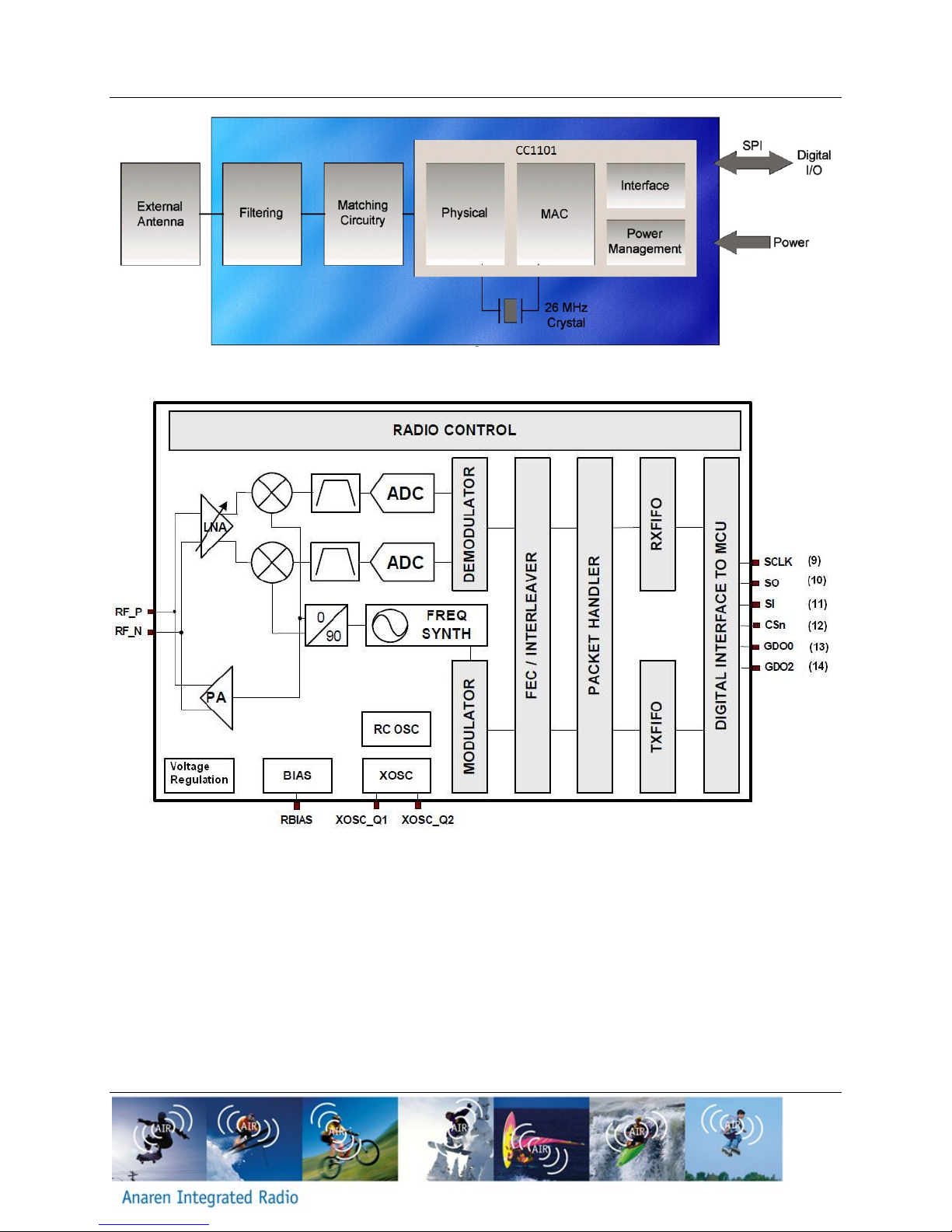
1.2. Theory of Operation..................................................................................................................................6
1.2.1. Typical Flow........................................................................................................................................8
1.3. Configuration...........................................................................................................................................10
1.4. Applications.............................................................................................................................................10
2. Approvals and Usage ...................................................................................................................................12
2.1. Product Approvals..................................................................................................................................12
2.1.1. Europe (Conformité Européenne, )...............................................................................................12
2.2. Potential Interference Sources ...............................................................................................................13
2.2.1. Time critical data...............................................................................................................................13
2.3. Approved Usage .....................................................................................................................................13
2.3.1. Europe ...............................................................................................................................................13
3. Electrical Characteristics ..............................................................................................................................16
3.1. Absolute Maximum Ratings ..................................................................................................................16
3.2. Operating Conditions .............................................................................................................................17
3.3. Pin Out......................................................................................................................................................17
3.4. Recommended Layout (Dimensions in mm)......................................................................................19
3.5. Power Supply Considerations...............................................................................................................19
4. Mechanical and Process................................................................................................................................20
4.1. Radio Module Details (Dimensions in mm) .......................................................................................20
4.1.1. A1101R04C.......................................................................................................................................20
4.2. Packaging Details (Dimensions in mm) ..............................................................................................21
4.2.1. Matrix Tray Packaging .....................................................................................................................21
4.2.2. Tape-Reel Packaging .........................................................................................................................21
4.3. Soldering...................................................................................................................................................22
4.3.1. Manual Mounting Procedure ...........................................................................................................22
4.3.2. Automated Mounting Procedure ......................................................................................................23

THIS PAGE LEFT INTENTIONALLY BLANK

A1101R04C –User’s Manual Page 5 of 26
Release Date 02/20/12
1. Overview
The A1101R04C is a surface mount module with an integrated crystal, internal voltage
regulator, matching circuitry and filtering. The A1101R04C utilizes an external antenna through
a U.FL connector (see Table 1). The module operates in the European band of 433.05 to
434.79 MHz, is ideal for achieving low power wireless connectivity without having to deal with
extensive RF design and regulatory compliance, and provides quick time to market. The
modules are 100% tested to provide consistent performance.
The A1101R04C has received regulatory approvals for modular devices in Europe (ETSI). The
modular approval allows the OEM or end user to place A1101R04C with an approved antenna
inside a finished product without having to perform costly regulatory testing for an intentional
radiator. Section 2 has information on the requirements the end user/integrator must fulfill to use
the modules without intentional radiator regulatory testing.
The A1101R04C is based on the CC1101 transceiver IC from Texas Instruments. All control
lines for the transceiver are provided at module level for full control of its operation. Please see
the CC1101 data sheet (www.ti.com) for how to control the modules. Please see section 2.3 for
the recommended register settings to achieve optimal performance and regulatory compliance.
The A1101R04C has a compact antenna connector that allows for locating the antenna away
from the module due to form/function or in order to exit a metal enclosure.
The A1101R04C module measures 9x12x2.5mm.

Page 6 of 26 A1101R04C –User’s Manual
Release Date 02/20/12
1.1. Features
Features:
Frequency range: 433.05 –434.79
MHz
Ultra small package size 9mm x 12mm
x 2.5mm
Impedance controlled multi-layer PCB
Shielded Package
1.8 to 3.6 V operation
SPI Interface
RoHS Compliant
LGA Footprint
Low Power Consumption
Regulatory compliance for ETSI
Digital RSSI output
Programmable channel filter bandwidth
Programmable output power up to +12
dBm
High sensitivity (–116 dBm at
0.6kBaud, 1% packet error rate)
Low current consumption (15.7 mA in
RX, 250 kBaud, input well above
sensitivity limit)
Separate 64-byte RX and TX data
FIFOs
Fast startup time: 240us from SLEEP
to Rx or Tx mode
Data Rate: 0.6 –600 Kbit/Sec
Sleep state: 0.2uA
Idle State: 1.7mA
Benefits Summary:
Operating temperature -40 to +85C
100% RF Tested in production
Common footprint for all family
members
No RF engineering experience
necessary
Only requires a 2 layer PCB
implementation
Excellent receiver selectivity and
blocking Performance
Suitable for frequency hopping and
multichannel systems due to a fast
settling frequency synthesizer with 75
us settling time
Suited for systems compliant with EN
300 220
No regulatory “Intentional radiator”
testing is required to integrate module
into end product. Simple certification
labeling replaces testing.
1.2. Theory of Operation
The A1101R04C is designed for low power wireless applications in the European band of
433.05 MHz to 434.79 MHz. It can be used to implement a variety of networks, including point
to point, point to multipoint, peer to peer and mesh networks.
The A1101R04C interfaces to an application microcontroller via an SPI bus. Physical and MAC
layer functionality are accessed via the SPI bus, through addressable registers as well as
execution commands. Data received or to be transmitted are also accessed through the SPI bus
and are implemented as a FIFO register (64 bytes each for Tx and Rx).
To transmit, a frame of data is placed in the FIFO; this may include a destination address. A
transmit command is given, which will transmit the data according to the initial setup of the
registers. To receive data, a receive command is given, which enables the unit to “listen” for a

A1101R04C –User’s Manual Page 7 of 26
Release Date 02/20/12
transmission and when one occurs put the received frame in the FIFO. When neither transmit
nor receive is required, the device can enter either an Idle mode, from which it can quickly re-
enter receive or transmit mode, or a low power sleep mode, from which a crystal startup is also
required prior to transmit or receive operation.
Below a block diagram is given for the A1101R04C module.
Antenna
oThe antenna couples energy between the air and the AIR module. For
applications where installations are done by an end user (non-professional), an
omni-directional antenna pattern is desired, such that the application will work
equally well in any direction. Similarly for peer to peer or point to multipoint
applications an omni-directional pattern is desired such that all nodes have a fair
chance of communicating. The A1101R04C has an approved near omni-
directional monopole antenna listed in Table 1. Note that the end radiation
pattern depends not only on the antenna, but also on the ground plane,
enclosure and installation environment.
Filtering
oFiltering removes spurious signals to comply with regulatory intentional radiator
requirements.
Matching
oMatching provides the correct loading of the transmit amplifier to achieve the
highest output power as well as the correct loading for the receive LNA to
achieve the best sensitivity.
Physical
oThe physical layer provides conversions between data, symbol and RF signal.
MAC
oThe MAC layer is part of the Logical Link Layer and provides frame handling,
addressing and medium access services.
Microcontroller Interface
oThe microcontroller interface exposes registers and commands for the physical
and MAC layers to a microcontroller.
Power Management
oPower management ensures a stable supply for the internal functions as well as
providing means for a low power sleep mode (in which case, most of the
transceiver is power off).
Table 1 Approved Antenna
Item
Part Number
Manufacturer
Type
Gain
(dBi)
1
66089-0406
Anaren
Monopole whip, 173mm lead
3

Page 8 of 26 A1101R04C –User’s Manual
Release Date 02/20/12
Figure 1 The functionality of the A1101R04C, using an external antenna.
Figure 2 Transceiver IC block diagram.
1.2.1. Typical Flow
After initial setup of registers for desired behavior, the normal operation flow diagram is shown
in Figure 3 . In applications of infrequent data transmissions the transceiver would be in “sleep”
mode to save power (200nA). From there it would awaken and then enter “idle” mode. As part of
the wake up process the crystal oscillator is started (~240μs) and the digital microcontroller
interface is powered up. Before transmit or receive, the frequency synthesizer needs to be
started (“FS_Wakeup”) and, having been powered off (or idle for a while), the control loop of the
VCO/PLL needs to be calibrated (“calibrate”).

A1101R04C –User’s Manual Page 9 of 26
Release Date 02/20/12
A data frame is loaded into the transmit FIFO and the “TX” mode is entered. The transceiver will
transmit the data and enter “idle” mode after completion. When transmit is complete “RX” mode
is entered to wait for the acknowledge frame. Once a frame is received the transceiver will again
enter “idle” mode. If no acknowledge frame is received within a given timeout the data frame
would be re-transmitted. If the acknowledge frame indicates that the data was received the next
data frame will be transmitted. After the last data frame has been transmitted successfully, the
transceiver will again be put in “sleep” mode.
Figure 3 Transceiver state diagram

Page 10 of 26 A1101R04C –User’s Manual
Release Date 02/20/12
1.3. Configuration
Table 2 lists the radio module configuration parameters, and the level of configurability by the
user.
Legend:
1.4. Applications
Ultra low-power wireless applications, operating in the 433.05 –434.79 MHz ISM/SRD bands:
Wireless alarm and security systems
Industrial monitoring and control
Wireless sensor networks
AMR –Automatic Meter Reading
Home and building automation
Existing applications where simple upgrade to wireless is desired
Certification is valid for any value choosen
Use the provided certified settings as other may degrade performance
Any modification of this value is a violation of the certification and the
customer is responsible for optaining their own certification
Unused/undocumented function. The provided default value must be written.
No assumption should be made on the value read from this field
Read only register (burst mode read only, command strobes otherwise).

A1101R04C –User’s Manual Page 11 of 26
Release Date 02/20/12
Table 2 Configuration Parameters
Register Name
Register
Address
(Hex)
Retained
during
sleep
7 6 5 4 3 2 1 0
IOCFG2 00 1 0 GDO2_INV
IOCFG1 01 1 GDO_DS GDO1_INV
IOCFG0 02 1GDO0_TEMP_SENSOR_ENABLE GDO0_INV
FIFOTHR 03 1 Reserved ADC_RETENTION
SYNC1 04 1
SYNC0 05 1
PKTLEN 06 1
PKTCTRL1 07 1 0 CRC_AUTOFLUSH APPEND_STATUS
PKTCTRL0 08 1 0 WHITE_DATA 0 CRC_EN
ADDR 09 1
CHANNR 0A 1
FSCTRL1 0B 1 0
FSCTRL0 0C 1
FREQ2 0D 1
FREQ1 0E 1
FREQ0 0F 1
MDMCFG4 10 1
MDMCFG3 11 1
MDMCFG2 12 1DEM_DCFILT_OFF MANCHESTER_EN
MDMCFG1 13 1 FEC_EN
MDMCFG0 14 1
DEVIATN 15 1 0 0
MCSM2 16 1 RX_TIME_RSSI RX_TIME_QUAL
MCSM1 17 1
MCSM0 18 1 PIN_CTRL_EN XOSC_FORCE_ON
FOCCFG 19 1FOC_BS_CS_GATE FOC_POST_K
BSCFG 1A 1 BS_POST_K BS_POST_KP
AGCCTRL2 1B 1
AGCCTRL1 1C 1 0 AGC_LNA_PRIORITY
AGCCTRL0 1D 1
WOREVT1 1E 1
WOREVT0 1F 1
WORCTRL 20 1 RC_PD RC_CAL 0
FREND1 21 1
FREND0 22 1 0
FSCAL3 23 1
FSCAL2 24 1VCO_CORE_H_EN
FSCAL1 25 1
FSCAL0 26 1 0
RCCTRL1 27 1 0
RCCTRL0 28 1 0
FSTEST 29 0
PTEST 2A 0
AGCTEST 2B 0
TEST2 2C 0
TEST1 2D 0
TEST0 2E 0VCO_SEL_CAL_EN TEST0[0]
2F
PARTNUM 30 1
VERSION 31 1
FREQOFF_EST 32 0
LQI 33 0CRC_OK
RSSI 34 0
MARC_STATE 35 0
WORTIME1 36 0
WORTIME0 37 0
PKTSTATUS 38 0CRC_OK CS PQT_REACHED CCA SFD GDO2 GDO0
VCO_VC_DAC 39 0
TXBYTES 3A 0TXFIFO_UNDERFLOW
RXBYTES 3B 0RXFIFO_OVERFLOW
RCCTRL1_STATUS 3C 0
RCCTRL0_STATUS 3D 0
PATABLE 3E 1
FIFO 3F 0
Bit Fields Within Register
SYNC_LSB
PACKET_LENGTH
PQT
ADR_CHK
PKT_FORMAT
LENGTH_CONFIG
GDO2_CFG
GDO1_CFG
GDO0_CFG
CLOSE_IN_RX
FIFO_THR
SYNC_MSB
FREQ[15:8]
FREQ[7:0]
CHANBW_E
CHANBW_M
DRATE_E
DRATE_M
DEVICE_ADDR
CHAN
0
FREQ_IF
FREQOFF
FREQ[23:22]=0
FREQ[21:16]
DEVIATION_E
DEVIATION_M
0
RX_TIME
0
CCA_MODE
RXOFF_MODE
TXOFF_MODE
MOD_FORMAT
SYNC_MODE
NUM_PREAMBLE
0
CHANSPC_E
CHANSPC_M
BS_PRE_K
BS_PRE_KP
BS_LIMIT
MAX_DVGA_GAIN
MAX_LNA_GAIN
MAGN_TARGET
0
FS_AUTOCAL
PO_TIMEOUT
0
FOC_PRE_K
FOC_LIMIT
EVENT0[15:8]
EVENT0[7:0]
EVENT1
WOR_RES
LNA_CURRENT
LNA2MIX_CURRENT
LODIV_BUF_CURRENT
MIX_CURRENT
CARRIER_SENSE_REL_THR
CARRIER_SENSE_ABS_THR
HYST_LEVEL
WAIT_TIME
AGC_FREEZE
FILTER_LENGTH
0
FSCAL2
0
FSCAL1
FSCAL0
RCCTRL1
0
LODIV_BUF_CURRENT_TX
PA_POWER
FSCAL3[7:6]
CHP_CURR_CAL_EN
FSCAL3[3:0]
TEST0[7:2]
PARTNUM
VERSION
FREQOFF_EST
LQI_EST
RSSI
RCCTRL0
FSTEST
PTEST
AGCTEST
TEST2
TEST1
NUM_RXBYTES
RCCTRL1_STATUS
RCCTRL0_STATUS
PATABLE
TXFIFO/RXFIFO
MARC_STATE
TIME[15:8]
TIME[7:0]
VCO_VC_DAC
NUM_TXBYTES

Page 12 of 26 A1101R04C –User’s Manual
Release Date 02/20/12
2. Approvals and Usage
The A1101R04C has been designed to meet most national regulations for world-wide ISM-band
use. In particular the radio modules have been certified to the following standards.
2.1. Product Approvals
2.1.1. Europe (Conformité Européenne, )
The A1101R04C module has been certified for use in European countries. The following testing
has been completed:
Test standard ETSI EN 300 220-2 V2.3.1 (2010-02)
Frequency Error
Conducted Average Power (10% and 100% Duty Cycle Operation)
Effective Radiated Power
Spread Spectrum Spectral Power Density
Transient Power
Modulation Bandwidth
TX/RX Spurious Emissions
Test standards ETSI EN 301 489-3 V1.4.1 (2002-08), ETSI EN 62311:2008 and ETSI EN
60950-1:2006
Radiated Emissions
Electro-Static Discharge
Radiated RF Susceptibility
A helpful document that can be used as a starting point in understanding the use of short range
devices (SRD) in Europe is the European Radio Communications Committee (ERC)
Recommendation 70-03 E, downloadable from the European Radio Communications Office
(ERO) http://www.ero.dk.
The end user is responsible for ensuring compliance with harmonized frequencies and labeling
requirements for each country the end device is marketed and sold.
For more information see:
Radio And Telecommunications Terminal Equipment (R&TTE)
http://ec.europa.eu/enterprise/rtte/index_en.htm
European Conference of Postal and Telecommunications Administrations (CEPT)
http://www.cept.org/
European Telecommunications Standards Institute (ETSI) http://www.etsi.org/
European Radio Communications Office (ERO) http://www.ero.dk/

A1101R04C –User’s Manual Page 13 of 26
Release Date 02/20/12
2.2. Potential Interference Sources
Systems similar to the user’s system may also exist within range and may also be a source of
interference; some typical applications to consider are:
Alarm systems
oThese typically use low duty cycles and are therefore easy to avoid using
acknowledge/retransmit methods
Car alarms (internal motion sensors)
Weather stations.
2.2.1. Time critical data
If the user requires specific time critical data throughput that cannot tolerate the delays of
potentially many re-transmissions, the user is encouraged to implement an environment-aware
algorithm that periodically monitors/scans the frequency band and maintain a list of “best
available” channels.
2.3. Approved Usage
The radio modules can be used in a variety of physical layer configurations. The following
restricts the use to maintain compliance with the above-referenced certification bodies.
The user is encouraged to use minimum power required to establish a link, thus minimizing
interference.
Changes or modifications to the module and/or operation outside the limits set forth below are
prohibited and could void the user’s authority to operate the modules.
Uses of these radio modules are limited to the specified frequency ranges and configuration
settings. Using the radio modules outside of these limitations are prohibited and could void the
user’s authority to operate the modules. The register setting files for these configurations are
provided online at www.anaren.com.
2.3.1. Europe
Table 3 shows the approved configurations for use in Europe.
The maximum output power is 10 mW (10 dBm) if the module operates on a 10% Duty Cycle. If
100% Duty Cycle operation is desired, then the output power should be limited to 1 mW (0 dBm)
for the signals with less than 250 kHz BW, and -13 dBm/10 kHz for the signals with greater than
250 kHz BW.
In order to comply with the output power limitations in Europe, the maximum values given in the
tables below should be observed. Table 4 is for 10% Duty Cycle operation where higher power
levels can be used. The first number in each cell indicates the power level in dBm, and the one
inside the parenthesis is the PA Table value that is written to the transceiver chip.

Page 14 of 26 A1101R04C –User’s Manual
Release Date 02/20/12
Table 3 Approved European configurations
Table 4 Maximum output power (10% duty cycle)
Table 5 is for 100% Duty Cycle operation where a continuous transmission is possible. In this
case, the output power is lowered, and in wideband case (BW greater than 250 kHz), power
spectral density requirements are observed.
Table 5 Maximum output power (100% duty cycle)
Code Modulation Type Datarate(kbps) Deviation(kHz)/ PhaseTransition Time (Tb)
M1 MSK 500 5/8 Tb
M2 MSK 100 5/8 Tb
M3 MSK 38 5/8 Tb
M4 2-FSK 1.2 25.4
M5 2-FSK 10 34.9
M6 GFSK 10 12.7
M7 GFSK 38 17.5
M8 GFSK 100 44.4
M9 4-FSK 250 114.3
M10 4-FSK 500 203/228.5 (Tx/Rx)
M11 2-FSK 0.6 15.9
M12 GFSK 4.8 12.7
M13 GFSK 19.2 12.7
M14 4-FSK 600 228.5/253.9 (Tx/Rx)
M15 MSK 600 5/8 Tb
MN1 2-FSK 0.6 5.2
MN5 4-FSK 2.4 5.2
MN6 GFSK 1.2 5.2
MN8 4-FSK 20 19
MN11 4-FSK 153.6 32
MN12 GFSK 76.8 32
MN14 4-FSK 200 47
Modulation Code Low Temp [dBm (Hex)] Room Temp [dBm (Hex)] High Temp [dBm (Hex)]
All Modulation Types 8.3 (C9) 9.4 (C6) 9.7 (C5)
10 % Duty Cycle
Modulation Code Low Temp [dBm (Hex)] Room Temp [dBm (Hex)] High Temp [dBm (Hex)]
M1 1 (8C) 1 (8C) 1.7 (8B)
M2 -6.5 (2B) -5.3 (2D) -4.3 (66)
M9 -1 (51) -0.5 (60) -0.8 (8E)
M10 1.7 (8B) 1.7 (8B) 2.5 (89)
M14 1.7 (8B) 2.5 (89) 3.7 (87)
M15 1.7 (8B) 1.7 (8B) 2.5 (89)
All other types -2 (53) -1.5 (40) 0 (50)
100 % Duty Cycle

A1101R04C –User’s Manual Page 15 of 26
Release Date 02/20/12
The A1101R04C output power changes with ambient temperature. To obtain best possible
range and at the same time maintain certification compliance it is possible to trim the output
power as a function of temperature to maintain an approximate constant output power over
temperature. This can be done by changing the output power according to Table 6. The same
information is provided graphically in Figure 4. Note that the power level mentioned is the power
level one would measure at room temperature (i.e. the power level is in fact not increasing with
temperature, but is kept relatively stable when implementing this feature). If temperature
dependent control is not implemented the user must use the lowest power value for all
temperatures in order to maintain power within certification limits. A breakdown of the
temperature levels is given below for each Duty Cycle operation.
Table 6 Power adjustment for temperature
A graphical view of these levels is also provided in the chart below.
-6.5
-4.5
-2.5
-0.5
1.5
3.5
5.5
7.5
9.5
11.5
-40 -20 0 20 40 60 80
10% Cuty Cycle
M1 - 100% Duty Cycle
M2 - 100% Duty Cycle
M9 - 100% Duty Cycle
M10 - 100% Duty Cycle
M14 - 100% Duty Cycle
M15 - 100% Duty Cycle
All others - 100% Duty Cycle
Figure 4 Output Power over temperature
10 % Duty Cycle
Temp Range (Co)All Modulations M1 M2 M9 M10 M14 M15 All Others
(-40, -20) 0xC9 0x8C 0x2B 0x51 0x8B 0x8B 0x8B 0x53
(-20, 55) 0xC6 0x8C 0x2D 0x60 0x8B 0x89 0x8B 0x40
(55, 85) 0xC5 0x8B 0x66 0x8E 0x89 0x87 0x89 0x50
100 % Duty Cycle

Page 16 of 26 A1101R04C –User’s Manual
Release Date 02/20/12
3. Electrical Characteristics
3.1. Absolute Maximum Ratings
Under no circumstances must the absolute maximum ratings given in Table 7 be violated.
Stress exceeding one or more of the limiting values may cause permanent damage to the
device.
Table 7 Absolute maximum ratings
Parameter
Min
Max
Unit
Condition/Note
Supply Voltage (Vdd)
-0.3
3.9
V
All supply pins must have the
same voltage
Voltage on any digital pin
-0.3
Vdd+0.3,
max 3.9
V
RF input power
+10
dBm
Storage Temperature
-50
150
˚C
Solder reflow temperature
260
˚C
According to IPC/JEDEC J-STD-
020D
ESD
750
V
According to JEDEC STD 22,
method A114, Human body
model
ESD
400
V
According to JEDEC STD 22,
C101C, Charged Device Model
(CDM)
Caution!
ESD sensitive device. Precaution should be
used when handling the device in order to
prevent permanent damage.
Caution!
This assembly contains moisture sensitive
devices and requires proper handling per
IPC/JEDEC J-STD-033

A1101R04C –User’s Manual Page 17 of 26
Release Date 02/20/12
3.2. Operating Conditions
Table 8 Operating conditions
Parameter
Min
Max
Unit
Condition/Note
Supply Voltage (Vdd)
1.8
3.6
V
Temperature Range
-40
+85
˚C
3.3. Pin Out
The A1101R04C radio module shares a common pin-out and foot print with other Anaren
modules using different frequencies, thus enabling easy changeover from one to another, e.g. if
changing the frequency, antenna scheme, or adaptive antenna tuning is desired. Below the
common footprint is shown.
Figure 5 Pin Out
NC = NO Connection. Pin is NOT
connected internally.
DNC = Do Not Connect. Internal
connection used during assembly, do not
connect.

Page 18 of 26 A1101R04C –User’s Manual
Release Date 02/20/12
Table 9 Pin descriptions
Pin #
Pin Name
Pin Type
Description
1
DNC
NC
Internal GND connection used during testing, not recommended to
connect to main GND.
2
DNC
NC
Internal RF output connection used during test. Connecting this pin
to anything will require recertification for intentional radiators.
3
DNC
NC
Internal GND connection used during testing, not recommended to
connect to main GND.
4
NC
NC
Pin is not connected internally, but is reserved for future expansion.
It is recommended not to connect this pin to anything.
5
NC
NC
Pin is not connected internally, but is reserved for future expansion.
It is recommended not to connect this pin to anything.
6
NC
NC
Pin is not connected internally, but is reserved for future expansion.
It is recommended not to connect this pin to anything.
7
Vdcoup1
Analog
Optional decoupling of the modules internal Vdd supply. It is
recommended to not connect anything to this pin. In particular noisy
environment this pin can be used to further reduce the noise on the
modules internal Vdd, please see section 3.5 for further information.
8
GND
Ground
One of two primary ground pins
9
SCLK
Digital Input
SPI bus clock signal
10
MISO/GDO1
Digital
Output
SPI bus data out from radio when CSN is low, and general purpose
I/O pin when CSN is high
11
MOSI
Digital Input
SPI bus data into radio
12
_CSN
Digital Input
SPI bus select (active low)
13
GDO0
Digital I/O
(Analog
output)
General purpose port
14
GDO2
Digital I/O
General purpose port
15
Vdcoup2
Analog
Optional decoupling of the modules internal Vdd supply. It is
recommended to not connect anything to this pin. In particular noisy
environment this pin can be used to further reduce the noise on the
modules internal Vdd, please see section 3.5 for further information.
16
NC
NC
No Connect, the pin is not connected internally, but is reserved for
future expansion. It is recommended not to connect this pin to
anything.
17
GND
Ground
One of two primary ground pins
18
Vdd
Power
Supply
Power supply pin
19
NC
NC
Pin is not connected internally, but is reserved for future expansion.
It is recommended not to connect this pin to anything.
20
NC
NC
Pin is not connected internally, but is reserved for future expansion.
It is recommended not to connect this pin to anything.
21
NC
NC
Pin is not connected internally, but is reserved for future expansion.
It is recommended not to connect this pin to anything.
22
DNC
NC
Internal GND connection used during testing, not recommended to
connect to main GND.
23
DNC
NC
Pin is not connected internally, but is reserved for future expansion.
It is recommended not to connect this pin to anything.
24
DNC
NC
Internal GND connection used during testing, not recommended to
connect to main GND.

A1101R04C –User’s Manual Page 19 of 26
Release Date 02/20/12
3.4. Recommended Layout (Dimensions in mm)
Figure 6 Recommended PCB layout.
3.5. Power Supply Considerations
Noise on the power supply line reduces the sensitivity of a receiver and modulates onto a
transmitters signal, both of which causes a degradation of link quality and hence a reduction in
range.
The A1101R04C radio module has an integral ferrite bead in the supply line from pin 18 (Vdd)
and a decoupling capacitance to reduce any noise on the incoming power supply line. This
arrangement will eliminate most supply voltage noise. In particular noisy environments
(switching regulators, motor controls, etc.), it may be necessary to add additional noise
reduction means.
Pin 7 (Vdcoup1) is connected to the module’s internal supply line after the ferrite bead and
decoupling capacitors and can be used to probe the noise at module level. The noise level
measured on pin 7 should not exceed 120mVpp when in transmit or receive mode, it may
however exceed this value when setting up or accessing data to/from the FIFO’s while not
actively transmitting or receiving.
If the level measured is exceeding the above limit, steps should be taken to ensure maximum
range, including:
Adding decoupling capacitance to pin 7 (Vdcoup1).
Adding additional filtering in the supply line.
Adding an LDO in the supply line (the TPS734xx low Dropout Regulator from TI is
recommended).

Page 20 of 26 A1101R04C –User’s Manual
Release Date 02/20/12
4. Mechanical and Process
4.1. Radio Module Details (Dimensions in mm)
4.1.1. A1101R04C
Figure 7 A1101R04C dimensions
Table of contents
Other Anaren Radio manuals

Anaren
Anaren A8520E24A91 User manual

Anaren
Anaren A2500R24x User manual

Anaren
Anaren A1101R04C00GM User manual

Anaren
Anaren A1101R09x User manual

Anaren
Anaren A2530E24x User manual

Anaren
Anaren A110LR09x User manual

Anaren
Anaren A8520E24A91 User manual

Anaren
Anaren A2541R24x User manual

Anaren
Anaren A1101R09 Series User manual