ARP 1601 User manual

imSEQUENCER MODEL 1601
;c(.'
ARP INSTRUMENTS, IN
320 Needham Street
Newton, MA* 02164
617
DoGument Number 9001901
©SeptemtMr 1976, AJRP INSTRUMENTS, INC.
The information Contained herein isconfidentsajl and proprietary to arp nstruments. inc. itjs
DISCLOSED to YOU SOLELY ?OR PURPOSES OF INSTRUCTION AS TO OPERATION OF THE EQUIPMENT AND
MAINTENANCE AS APPROPRIATE. IT IS KOT TO BE USED BY YOU FDfR ANY OTHER PURPOSE, NOR IS IT TO BE
disclosed to OTHERS WITHOUT THE EXPRESS PERMISSION OF ARP INSTRUMENTS, INC.

SEQUENCER MODEL 1601
TABLE OF CONTENTS
INTRODUCTION
1.1 ProdlJCt Dascrimicii .*..2
1.2 Specifications .,2
1.3 Function Descript^ .^,3
2. THEORY OF OPERATION
2. 1S€quenc«r .4
22 O^iantiz^r 4
3. CIRCUIT
21
3.2
23
24
2B
3.6
3.7
28
3J&
210
3J1
212
213
214
215
216
OESCRIPTIONS
SEQUENCER
Clock On/Off. * * .5
One Shot *5
Clock Oscillator -5
Randomizer, Skip &Reset *.6
M-ask Circurt 6
Stfip .6
Foot Switch Jack 6
Counter/Latch 6
Decoder *6
Gate Output Processing *,*.*7
QUANTIZER
Current Source fit Semitone Shift 7
CV Generator 8t Scanner 7
Counter .,.7
Comparator *.7
Sample Control 7
External CV Input *,,.7
4.
SEQUENCER TEST POINTS 8,9
5. CALIBRATIONS 10,11
6. ASSEMBLY^DISASSEMBLY 11
7.
BLOCK DIAGRAM .,.112
8.
GENERAL INFORMATION {COSMOS Integrated Circuit} ... 13
9,
SCHEMATICS &LAYOUTS ............. 14,15,16,17,18,19
10.
PARTS LIST 22

SECTION 1INTRODUCTION
1.1 Product Description
The ARP Seciuencer, model 1601, i$ a16 st€p se-
quential voltage generator. Avoltage Icrvel slider is
provided for eoch of the 16 steps to adjust the volt-
aQe output from 0to -i-IQ volts. The sequencer may
be used in a*'6 X2'* mode so that outputs 1through
8(bank A) arid 9through 16 (bank B) ssquetice in
parailel. Tho outputs of banlOi Aand Bare prewired
to 6voyage qunntizer which effectively '^rconds
off" the sequencer's voltagn to the rusarest whole
twelfth of a volt. This allows precisa tuning since all
ARP products are tuned to a1volt per octave stand-
ard (1/12 volt per semitone).
Alow frequency voltage controlled deck governs the
stepping spaod of the sequencer and can be started,
stopped, gated, or speeded up eitner mariually or
externally.
Position gates provide aconstant voltage output
(+10 vo^ts) for as lor>g as the sei^encrer ^on a
selected position. The positiors gate outputs are
bused to one of the position gate outputs (Gate 1,
2. or 3).
TJZ Specifications
SEQUENCER
Step, Reset, Start, Sftjp end SOft/Sunp
4
/ack inputs Accepts +3 Vto +10 VGate
CLOCK
Type. .Voltage Controlled
Pu/w WSdfft 4..*,10% to 1D0% (6gss 5msec.)
PMf {Puise Wsdifi Modulation)
inputjsck Accepts Oto +IOvoKs
frequency Hsnoa 0.2 Hz. to 100 Hz,
PM input Senudvitf ........ 2V/0CT max*
dock Oo^ut +14 Vpulse wave
Warm Oo Drift 0
QUANTIZER
PofiCtkfn ."Rounds off" voltages to
nearest 1/12 V(semitone)
Martirtwm iriput Vo/fage (A&B) +1 0V
Numt>er ofpo^thm 16
Mwimtm Quantked CV
Output (A ^B) +2 V
Maximum (unguant/a^d) can^f
voitage output +12 V
Rangu 2octaves
POWER REQUIREMENTS
MdJtimum Gaa9 output voitaga +14 VLine Voitage,100 to 130 VAC
t$ X1Mode ..Channels Aand Bare common Line Frequency. 50-60 Ha,
8X2Mode .,.Channels Aand Bare separate
F/G, /./ C0/V/VfCT/CWS7OSK/VW£S/Zfi?
Uf& Umff coMrotr rn eacly position.
Power 20 Wans
Frssm 0*tt
To in*'- To^Vki'^

1.3 Function Description
iuenc0' mi ^
OG O 0
:RzR=n=;^z=!z'-zRzq^
-z-d-z-u-c-z-d==f=i
1»
•L- -li- -U- -It- •:]-
24 23
I
• 9 ...... jp
•••w*»w •« W9*•^!•* *
!--:- -'i* -i -
1
--1--
-y. -0-.y. -0-.u-
.
I^
21
22
94m
20
t;0;
^Tli'
ll
18 15 14
a#ma %
12
13
,10l I
11
Po'ittfM fiWCrAMv'
Suispli«t a+14 volt gatE to Ort* of ihr«e
>outpou.
^OtOf Ix>put: (Pear Pand) Sop-
pfi24 a+14 voJtgaU^ to tfje "foot Switch
Out" jack On the front psDnel.
Poi*tM>n Oata SUs Oi/prurt.'+Hvoftpate
ou(puu wtifch arc usually c^nnnjtad to
exTarne^ envelope g^^neratan.
P^jitioft tOutput: Supplies d+14 volt
ga«j on position 1(only) to synchronize
Bckfitionaf sequencers or synl+^siam.
Cfocke<f Gate Out: AMcws the tdectioff
of pefticular pceution qates fOate Bus 1)
wjih control of the puls vwdth lCio«k>.
6C/ock Out: a+14 veil clock
puise which cs^ trij^r external eirwkipe
qenereton.
7Ouantizeti OV C7u<p£/£r. Provides acon-
tre^ voitege in 1/12 volt jncrements (0 to
+2 volt ran^il whDch coittrols the pitch
of BxternaJ oscillators. The Aend 6out'
a
pu*;s si*a common in th$ 16 X1mode.
bu: separate in tfie 8X2mode.
8CV tn: AIIdvjs e^ternaf control vcftaqes
(fram akeyboard for example} to be
summBd with the sequencer's vottaqe to
shift the key in which the sequencer
plays,
9QitPntizar tnputi: Allows voltageoc to be
'^ijandzocT* {rounded to naan»st t/12
vo&L'). Prepatchfid to the sequencer out-
puts.
10 ^&r4i4eocer Ouipurs: Provides a0to +10
voft: aneiog contyol voltage.
12 Ptitsa WkithT Variss the pulse width of
the cfook,
13 dock F$4: AiCqwy eaiKmal control vcft*
apes tq increase the speed of the cK)ck
(prewirOd to Gate 6Ux) 1}.
14 dock Frequppcy: Mir^slly varies tha
clock rote from .2Ha td approx, lOQ Hz.
15 SPiftJStpp: /Ueemately starts ar>d stops
the sequencer.
16 Trig/Gata $witctt: Trigger mocte stlows
the sequencer 10 he '‘triggered^ CO. In
tha Goto mode, the lequencer is on
whrle tho start button la held.
11 Cammoft CQdvspience /ecAju
17Fxtan^Y sCPrtS tha »tru»rp™r,
18ExternoXv stPtn the eeqoeocer.
19 Step: Mmtaetdie sequencer to the
next poeilMiv.
20 ffeitr.* Riiwu tha sequoncar to position
1Isequential modeonlyl.
21 AlknMi particular posit\:»ns
(frem gate bus 3| to allhnr skip past or
reset on particular positions.
22 StmzePtM/Haodom Media: Allows clock
to eckreoce to eadD succassisre pocitlon or
edvatscetoagandompoirtion.
23 ilodb Switch: firapt the eequencer 16
time^ Or stepe toidce Aand B8times in
paaiUet.
"LCOt: (Light Emicbng Oiode;;) Indicates
wfeich pasitiqn is OA
25 Aui^'u/i Tutting SfidiRrs: Tunes individual
positions {adjusts CV level).

SECrrON 2THEORY OF OPERATION
2.1 Sequencer
The heart of the sequencer is the Counter/Latch
circuit which prx>duces efour bit binary numbar.
When initially reset, the output of the counter
is 0000 (Position 1cope), or zero. Each time the
counter receives apulse from the Mask circuit, the
counter 4^dvances to the next binary numtur (0001,
0010, 0011, 0100.„1tn). The highest binary
number, 1111, corresponds to position T6.
This code hsupplied to the Decoder circuit which
decodes the binary number to one of 16 outputs. For
example, when the code 0000 i$ present on the
output of the counter, the decoder will turn on the
position 1output (only); when the code 0001 is
present on the output of the counter, the decoder
will turn on only the position 2ootput, etc«
When in the '*8 X2" mode, athree bit code is
supplied from the counter instead of four. Positions
1through 8and 9through 16 in the Decoder circuit
simultaneousiy decode so dtat barK A(1-8) and
B(9-16) sequence in parafler
The -Voltage Cortrolled Low Frequency Clock
determines; when the counter is advanced to
the next position by pulsing aone shot circurt.
The one shot in turn supplies apuM to the Mask
circuit which advances the counter and dbabies
(masks) the gate outputs during the count advance.
counter
When the sequencxr is in the random mode, the
RarKfomizer circuit advances ihe counter at an
extremely high frequency. For each cyde of the
low frequency clock, aposition number on the
output of the counter is memorized and held until
the next clock pulse. Since the counter is being
advanced so fast, the pcesition numbers which are
memorized will be random.
2.2 Quantizer
Vottages whidi are to be quantized to the nearest
whole twelfth of avolt are appHed to the or
"8'' Input of the quantu»r,” One quantJz&r circuit
is multiplexed by switching bet/veen one of the two
tn|!uts (A and B) to provide two indeper>dont quan-
tized control voltage outputs. The voltages ere
quantized and stored extmmefy quickly, s# that
two dtfferer^t voltages arc quantized (one at a time)
fftstei* than csn be detected by the ear. A$ In a
standard keyboard, aresft^r chain of equal value
re^lKtors make up avoltage divider to generate a
volteye reference. The voltages produced by thb
reference CV generator are 01/1 2V, 2/1 2V,
3/12V...2V (2 octave range). Ahigh frequency
oscillator steps acounter whoch enables the CV
generator voltages to be "scanned" one at atime
(0 volts to 2volts}.
The Input voltage which is to be "quantized" is
compared to ihe reference CV on the scanner output:
if the scanner output is lower than the input voltage,
the counter advances until the scanner voltage Is just
higher than ihe input voltaEge. The counter kthen
stopped (by the Comparator circuit) and the voltage
on the output of the scanner is memorized. The
counter is then reset to zero so that the voltage on
other input nfiay be quantized naxt.
ABc D AB c o
SEQ/RAr4D. SWITCH
{IN SEQUCNTtAU
pQsrnoN)
no. 2. fstar^jAL flow DO 66 o o o
z34sc"^ 7'
6
ic 11 12 13 14 IS le
POSITION OUTPUTS (OPIVES LEDS CV SLIDERS)
4

nc,2,2 SEQUeNC€S OUmJTS
SECTIONS CIRCUIT DESCRIPTIONS
3.1 Ctock Oii/Oflf
GiUte si9nals applied to the start jack set the Qoutput
of Z2B to logj:: 1(-1-15. volts) and Qbar to lofiic 0
(0 volts). Gate signafs applied to thii stop jack set
the Qoutput of Z2B to logic 0and tho Qbar to logic
1, Each tirne agate signal is applied to the start/stop
jack or when the start/stop button is depressed, the
Qoutput of Z2B assumos the logic tevel of the Qbar
output so that the Qand Qbtar outputs reverse state.
Wien the Gale/Trjgger switch (52) is ir> the gate
position, the Oc>jtput will assume alogic 1state for
as long as agate kpresent on the start/stop jade.
Summary: For adock "on" stata, the Qoutput of
Z2B {B point) will be alogic VFor aclock "off"
state, the Qoutput is alogic 0.
3.2 One Shot
A4millisecond pufse occurs on the Qoutput of
Z11A when pul«d On tha Ainput (pin 5). The
pulse on tue output of the on* shot is supplied to:
1) tho Clock Oscillator to reset the sawtooth: 2} the
Resat circuit to fiin^then the external reset pulse (if
applied) when the Epoint is art alogic t; end 3)
the Randamixar dicuit to momenuirilv disable the
high frequency osciHator (random mode only).
3.3 Ctock CHaHlatar
Three circuits comprise the Clock Oscillator: the
Voltage ControilW Oscjllator, Sawtooth to Pulse
Convener, and Comparator.
Sawtooth Oscillator: Voltages from the deck FM
input jack and the dock rate slider are summed on

the of Q4. Q4 and Q5 are 0linear voltage to
exponential currant corrverter. Capacitor C7 is
initially charged to +15 volts and di:Echarges toward
ground through Q5, Z3A and Q7 follow the\x:i(tage
level on C7 and supply it to the oomoarator and the
sawtooth to pulse converter. The output of the
comparator {pin 13, 8J will switch to +15 volts (logic
1) when the sawtooth voltage falls below +7,5 volts.
The comparator output Is supplied to the one shot
which reset cacocitor C7 to +15 volts.
Sawtooth To Pulse Corrverter: Voltages from the
Pulse Width Modulation jack and the Pulse Width
slider are applied to Z4A and Z4B tz> set the dock
pulse width. The collector of 08 will be apulse wave
with apul&e width from 20% to 100% depending on
the pQsitk>n of the pulse width slider. The pulse
output of the choc< oscillator fe routed to the Gate
Output Processing urcuit {schematic 2
L
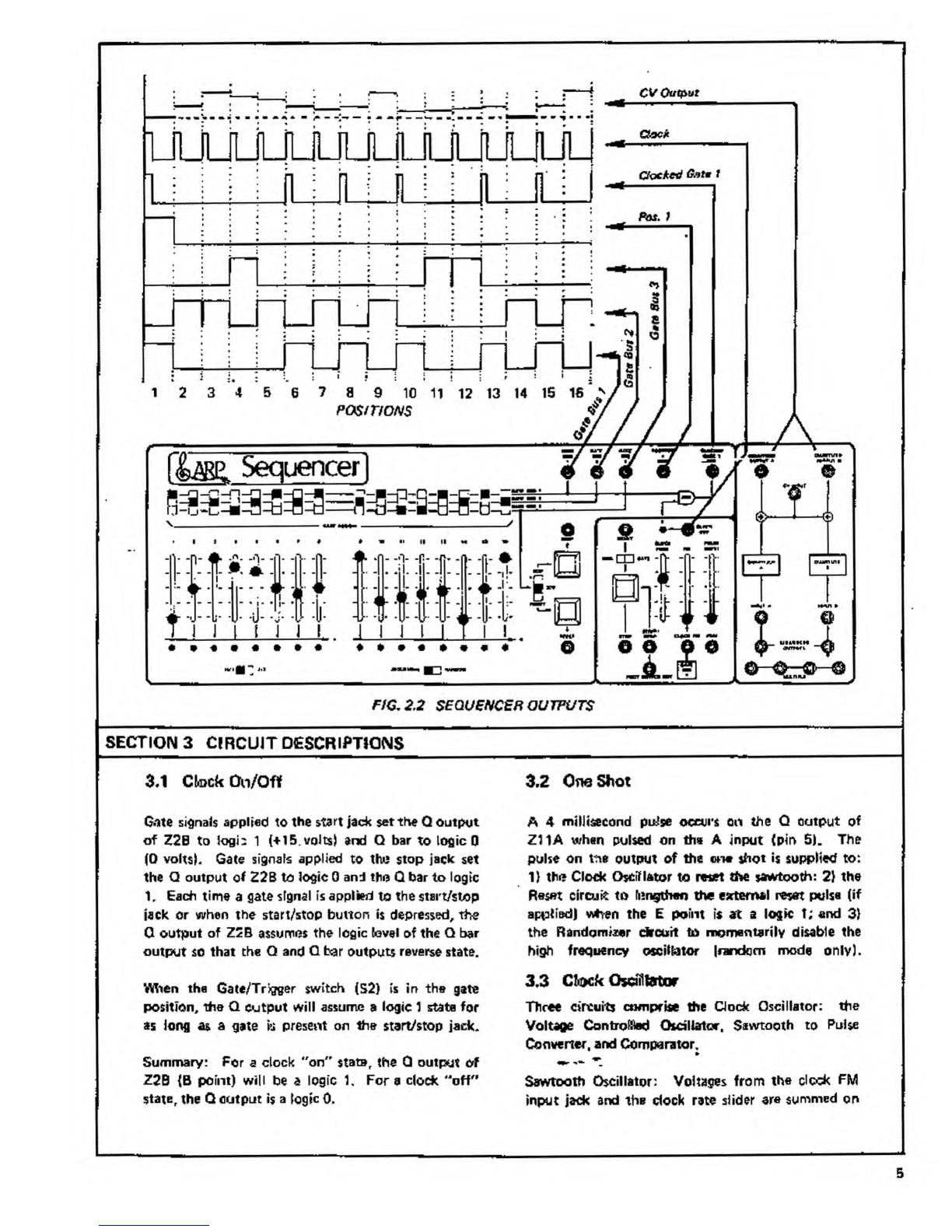
34 Randomize!, Skip &Reset
Z1 IB is ahigh speed oscillator Uppiox. 5mi{7osecJ.
Whan Z16A pin 3is alogcc 1, ZllB producesa high
frepuency pulse chain or\ pin 9. When 21 6Z pin 3is
at alogic 0(ground) 21 IB stops oscfllBting. With
slide switch S21 in the Random posrtkin, Z10C pin
10 will enable (turn on] the high speed oscillator
(Z11B) through 21 6A. Z11B will then provide a
pulse diain to Mask circuit. When pulsed by the
clock ccscMIator, the one shot will momentarily turn
off the high speed oscillator through ZtOC (pin 12 &
13) to allow the left»:rh in the Counter/Latch circuit to
memorize a{random) position, Duf ng this mode,
Z7B generates random voltage levels tg vary the fre>
quency of 2116 to insure arandom sampling of
positions. With S21 mthe Sequential mode, ZIGC
will not affect the frequency of the high speed
osciiEator, When S22 is in the skip position, pin 8
of Z9C is at logic 0. When the Jpoint Is also at a
logic 0, Z9C pin 10 the«n turns on the h’qh speed
Oscillator which quickly advances; the sequencer
to the next position (via 216C).
In the reset position, the gate signal on the Jpoint
is supplied through S22 to Z9D. When the Jpoint
is at logic 0, 290 supplies alogic 1which resets the
a>untcf to position 1via ZI6B. External reset gates
may be applied to 027 amf by depressing the reset
push button {S23).
3.5 Mask Circurt
Z15A pin 3is logic 1when the sequencer is in the
"sequentbl" mode which allows the latch (Z8) in
the Counter/Latch circuit to transmit data con*
tinuously. When pin 3of Z1SA es logic 0. (random
mode only) Z8 in the Counter/Latch circuit holds or
stores the dats on the counter output.
The one shot pulse will cause the Qand Qbar out-
puts of 22A to momenterily reverse 'state. The
output of the high speed oscillator (ZllB) and the
Qbar outpHJt of Z2A are then combined on Z16C
which advances the counter in the Counter/Lateh
circuit. A''mask^' pulse is generated by combinina
the one shot puMs (4 msec, duratoon) and the pulse
from Z2A (8 mkrosec, duration) on the output of
Z15B (pin 4) to turn off all the gate outputs during
the time the counter is advanced from one position
to the next.
3.6 Step
When gate sigrials are applied to the step jack or ftcm
the step push button, 26A pin 3provides apulse to
the One Shot circuit and the Gate Output Processing
circuit.
3«7 FcMit Switch Jack
The foot switch jack on the fror^t panel provides a
+10 volts gate for as long as the foot switch is held
and can be patched to any of the input jacks on the
front panel
3.8 Counter/Latch
Z7A kadivide by 16 counter providing a4bit code
to 28. 28 is alatch circuit but normally transmits
cfcjta to the Decoder circuit unaffected. Z9B and Z9A
are connected to the Qand Qbar outputs of ZB to
enable Z13 and Z14 in the Decoder circuit one at a
time (sequentiaily).
3.9 Decoder
213 and 214 decode the hcnary number from the
Latch circuit tc one of 16 positions, WhenS4fi is in
the 16 X1mode, Oil through 26 wilt turn on one at
atime sequentially (1 through 16). In the 8X2
mode, 213 and Z14 decode in paraliei (position
1-8 and 9-16). In the random mode, tha courier
advances at th<? rate of the High Speed Oscil^tor
(ZllB, schematic 1) but in this mode, Z8 holds
the code which is supplied to the decoders constant.
The strobe input of the 28 allows arandom binary
number to be memorized on each dock pulse which
is sjjpplied to the decoder.
Ql 1and 026 are turned on one at atime and supply
voltages to one of the three gate bus lines through the
three posieksn gate switohes. At the same time, the
LED is lit indicating which position is OfJ. The three
position sfide switches provide the path to ground
for the LEOs.

The voltages from the decoder chips are also sirpplied
to 100K sliders CR&7 through R103) ti> provide a
+10V) for each position.
Voltages from the Abank sliders and the Bbank
sliders are summed in the output amplifier circuit
Zl9A and Z18A_ When the sequencer is in the t6 X
1position, the output of the Aand 6channels are
summed together so that the cutpuU of Zl9B and
Z18B will be ths same. The Sequencer output
voltages supplied by the output amplifiers are routed
TO the quantizer (hematic 3|.
%
3.10 Gate Output Processing
Gate Output Processing circuit provides 6outputs;
Gate Bus 1, Gate Bus 2, Gate Bus 3, Clocked Gate
T, Clock Output, and Position 1Output,
The Gate Buts 1,2, and 3outputs are driven from the
3portion slide switches in the Decoder circuit.
Z15C and Z15D are afUpTtop which supplies the
Clocked Gate 1Output and turns on the clock
irxiicator Jic^ CCR22). The position toutput
obtains hs stynal from Position 1(QU base) in the
Decoder circuit so that rrrane dian or» sequencer
can be synchronizedL
QUANTIZER
3..1 1Current Source &%mitone Shift
Z29A supplies constant current through 13 equal
vafue resistors (lOOohml located in resistor pack
220. The voltage drop across each resistor h2/12
of 3volt semitones, or one whole tone). Q36
supplies an offtet voltage to pin 3of 229A to ''shift"
or raise the output of the current source (and there-
fore pins 1ifwough 14 of 220J up 1/T2 of avolt,
3*12 CV Generator &Scanner
Z21 and 222 are digitally controlled snalog switches
which are connected to the CV generator outputs
1Z20). The three binary inputs (A, Band C| select
one of eight switches to be turned on and corenect an
input (pins 13, 14, IB, t2, 1, 5, 2,or 4| to the output
(pin 3|* AJI of the switches are off when alogic 1is
0f> pin 6(inhiait). The A, Band Cinputs of Z2l
are driven by 225.
3.T3 COUNTER
225 generates abinary number which "courJts" from
OOCOQ to mil. The first bit (^B) inhibits either
221 or 222 so lhat only coe voltage from Z20 is ever
on at the sarne time. The next three bits (pins 6, 9,
and 11 of Z20) turn or> channels 13, 14, 15, 12, 1
etc, orjs at atime sequentially. The remaining
bit (LSB> on the Counter output (pin 12) is yjpplied
to the Current Source to shift the resistor cham le\'sl
up 1/12 of a\talt to obta.n two volta^J levels per
resistor in 220.
3,14
Comparator
9
The scanner output (2298 pin 7} is supplied to the
inverting input of the Comparator (Z22). An
external control voltage which is to be quantized
is supple to the ni3ninverting input of the Compara-
tor via the Inout Channel Selector.
Initially, the Corrtparator output is logic 1|+1B volts)
which permits the ooumer to be advanced by the
Clock through Z240. Mthe Coumer advances, the
vottage on pir> 2 of 223 ''steps" in t/12 volt incre-
ments umiJ it exceeds the voltage level on pfr> 3of
223, The output of the Comparator thun changes
to logic 0which immediately stops the Counter, The
voltage on the Scanner output (now constant) is the
nearest 1/12 of avolt level to the input control volt-
age; therefore, it is supplied to the Charnel Memory
vu 230C to be stored.
3.1 5Sample Control
230C is enabled when the Sample Control provides
alogic 1to the clock input of Z2BA. Z28A then
turns on one of the trensmissiort gates (either channel
Aor 8| for atime perk>d of half aclock cycle. Aflei'
the quant zed control voltage from Z29C has been
supplied to one of the memory circuits, 227C resets
both the Sample Control ai>d the Counter. Addi-
tiortally, the outputs of Z2BA reverse state to switch
from one channel to the other (A to 6for example).
The Quantizer is now ready to quantize the voltage
waitiiiQ on the other input.
3.16 External CV Input
The External CV input allows acontrol voltage from
another synthesizer to be summed with the output of
the two CLuantizer cincuits. The keyboard CV of
other instruments can be added to the sequencer's
voltage to change the key in which the saquancer
plays simply by playing an extsmit keyboard,
TTie i^t~points on the ^Komng two fVas^r&u
oparst/an of the cvrcu/ts mthe seguencer in
re^9t/on to one onather.
1

SECTION 4SEQUENCER TEST POINTS
TP-1
TP-2
TP^3
TP-4
TP-5
TP-6
TPJ
FUNCTION jsET UP
HIGH FREa
OSC. I1, Put the SEQ/RAND switch in
Ithe RANDOM nv>de.
I2. Put the SEQ/RANO switch in
the SEQUENTIAL mode.
CLOCK
ON/OFF I
1. Put the TRIG/GATE switch in
1tha GATE position. Depress the
STABT/STOP button.
$2, Put the TRIG/GATE switch in
the TRIGGER position. Depress
the START/STOP buttor>.
ONE SHOT 1, Put the CLOCK FREQ, slider at %.
2, Put all other sliders fully DOWN.
3, Start the Sequencer.
CLOCK
SAWTOOTH 1.PuttheCLOCK FREQ, slider at U.
2. Put all other slicers fuliy DOWN.
3. Start the Sequencer.
COMPAR-
ATOR 1. Put the CLOCK FREQ, slider at %.
2. Put all other sliders fully DOWN.
3. Start tha Sequencer.
CLOCK 1. Put the CLOCK FREQ, slider at
2. Put all other sUders fully DOWN,
3. St3rt the Sequencer,
4. Put tha PULSE WIDT>4 slider
fully up.
1. Put the CLOCK FREQ.
2. Put dll other sliders fully DOIIVN,
3. Start the Sequencer.
TP-8 MASK
ADVANCE 1. Put the CLOCK FREQ, slider at %
2. Put all other sliders fully DOWN,
3. Start the Sequercer.
TP-9 MASK 1. Puttha CLOCK FREQ, slider ^X%.
2. Put ell other sliders fully DOWN,
3. Start the Sequencer.
SPECIFICATIONS
0volts (constant)
$tBrt/Slop buttc/1 befd &own
Alternates betweert +15 Vand 0Vwhen START/STOP
is depressed.
4mstc.
2Smc4C. typical
+1 5^lU (constant)
(4 instc *ausec) Ji;
TP-10 ADVANCE 1. Put the CLOCK FRCa slider at
2. Put all other sliders fully DOWN.
3. Start lha Sequencer.

Thff fQ//owins pa^ts u$e the saws p^mef settings:
QUANTIZER
TEST
Point
TP-' 02
CLOCK
TP 12 (Zh
CLOCK
TP-13 SEM.
SHIFT
TP-14 SCANNER
A
TP-15 SCANNER
IB
TP-16 jSCANNER
C
TP-17 SCANNER
TP18
TP-19 JcOMPAR
IATOR
TP-20 SAMPLE
TP -21 RESET
i
4
1
^fO~E: TB$t pointi n-17 »1d 19-20
are +15 Vpulys waves.
1. Put if\tt SEQ/RAND switch in the SEQUENTIAL position
2. Put tha QATE/TRIG switch in Iha GATE
3. Put the mode switch in the 6X2 position.
4. Depress ine RESET button (position 1LED should he Irt)
5. Put the PvDSITION 1sikier about 1/3 up.
6. Put ihe POSITION 9sIxJer about 2/3 up.
FUNCTION ISPECJFICATIONS
ACHAN ACHAN, BCHAN.
eCV IW tEXAMPLH)
FROM SEQUENCER
ACV IN (EXAMPLE!
FROM OEQUENiCER

SECTION 6CALIBRATIONS
5.1 Sequencer &Quantizar
REF, NO. ITRI«/ir«)ER. TR3M FnOCEDURE
R19 FREQ. CAL,
R26
R206&
R207
PULSE WIDTH
AOFFSET*
eOFFSET
ADJUST
1. Put the CLOCK FREQUENCY SLIDER fully UP.
2. Monitor the CLOCK OUTPUT whh afrequency countCf or oscilloscope.
3. Put all other slidars fully DOWN.
4« Adjust trimmer R19fora tO f0s9C« period waysform {iQOHz.}.
1. Put ell GATE ASSIGNMENT v^ltchQi fully UP |Gat« Bus 1position),
2. Monitor the CLOCKED GATE 1OUTPUT with an os«Hlt«cope,
3. Put the GATE/TRIG switch \n the TRIGGER mode.
4. Depress the START/STCP button to g-^ART the sequesnoer.
5. Put the CLOCK FREQUENCY slkJer fully UP.
6. Put the CLOCK FM slider fully DOWN.
7. Put the CLOCK PULSE WIDTH slider fufly UP»
S. Turn trimmer R26 fully CLOCKWKSE.
9. SLOWLY tui'O trimmer R26 COUNTER CLOCKWPSE uotJI waveform
disappears (constant +14 vo(ts). TURN NO FURTHER.
1. Connect apatch cord from INPUT Ajack to INPUT Bjack (Isolates
quent^er InputsL
2. Adjust trimmer R20S for 0volU ±.005 Von QUANTIZED AOUTPUT.
3. Adjust trimmer R207 for 0volts ±.005 Von QUANTIZED 8OUTPUT.
R226&
R222 QUANTIZER
CV V/OCT
R217*
R218 AMOO ADJUST
0MOD ADJUST
1. Put all sliders on the sequencer fully DOWN.
2. Put the TRIG/GATE switch <n the GATE mode.
3. Put the sequencer mode switch in the T6 X1POSITION.
4. Put the SECVRAND switch in tfne SEQUENTIAL positron.
5. Depress the RESET button (position 1LED should be litl.
6. Put the PDSmON 1SLIDER fully UP.
7. Adjust trimmer R266 for '^2.00 vot^ on the QUANTIZED OUTPUT Ajack,
a. Adjust trimmer R222 for +2.00vofta on the QUANTIZED OUTPUT Black.
1»Put all the sliders on the sequencer fully DOWN,
2. Put the GATE/TRIG switch in the GATE mode,
3. Put the mode switch iai the 16 XtPOSITION.
4. Put the SEQ/RAND switch in thi> SEQUENTIAL po^itran.
5. Depress the RESET button (position 1LED should be (ctL
6. Connect apatch cord from INPUT A;ack to INPUT Bjack (isolates
quantizer inputs).
7. Monitor the ASEQUENCER OUTPUT with aDVM.
8. Raisa the POSITION 1SLIDER to
9. Measure and record the EXACT VOLTAGE lawl on the Asequencer output
(should be near +5 volts).
10. Connect apatch cord from the ASEQUENCER OUTPUT |ack to the
CViNjack.
11. Monitor tha QUANTIZER OUTPUT Awith aOVW.
12. Adjust trimmer R2I7 for EXACTLY the same vottage as measured in
step 9(unity gain)
,
13. Monitor the QUANTIZED OUTPUT 8with aDVM.
14. Adjust trimmer RZfBfor EXACTLY the same voltage as measured In
step 9(unity gain).
10

5.2 Powsr Supply
TRIMMER TRJM procedure
R5
R11
+5 VOLT SET
15 VOLT SET
1.
2,
1.
2,
Monitor the power supp1y*s +15 ^olt output with adigital voHmeter.
Adjust R5 for exactly +15.00 volts.
Set R5 {+15 volts) first.
Put the digital voUmeter's ground lead on the pow6v supply's -15 voft output
and put the meter^s plus lead on -,he power supply's ground output.
3. Adjust R11 for exactly +15.00 volts (reverfOd polarity).
SECTION 6ASSEMBLY/DISASSEMBLY
w
YYY
If
1,
To Prevent shock when trouble sfiooting, unplug
thfl sequencer and mount th« power supply on the
outside rear pgnel (t&e&tsDve tfhxs:iroifon).
2.
To remove tho main printed circuit board, remove
11bolts Wtustrsted abtwef, remove at\ dider krx>bs
on the fror>t panel, and gentjy push on lt>e drafts of
the sliders until the bc?ard pops loose.
3,
To remove the lower j^k board asseimbly, remove
the jack nuts on tba lower front panel. Then pull the
bottom of the power switch out so that the jack
board dears the power switch (see iUus^ration to
fc
11

UJ KJ
O
XX
SP
H
3
4^ 4A«iNr
.U>
yUJ *,
o-
iroc tIt
cc=^ 5X
=>S 5
0<^ M
in^Ni a
ANAh^ 04
9Ni?ilOO^d
mdiOO 31V0
^12 ISii
fi Sa«
zsna
rso*
X4VO
17*7
H77
S)13UndNV
indiop
iwr *
ANHMS QA
n
HDiV*l\b3lMft05
\^cr\7
IV
w
«e
Tb"
7^
«Q1VT>OSO
_
AJMM( 7*M»
12
$
X
O.Jt
SiS S3
I
xa«*%
X3S3U 3dl3tS
H3ZIVi0aN%b I^
¥*
lii
K
1601
SEQUENCER
BLOCK
DIAGRAM

ABC
I
I
AC0^
10
1 1 1
t
A-I
AC
C1
1
i
1
00
01
10
11
A
Ac
A00
01
10
1 1
Ac
1
1
CD44111AE
QUAD2WPUT
NANO ^9
HiIE
CMOS INTEGBATED CIRCUITS m
CD4001AE 9m Hfe f*N
f
QUAD 2tNPUT
NOB
I
aM»ITA
W9
ilfl
t
mmtL CL* V
t
CD4007AE *7.^
n.K-^T.i.f} 7
49
CD40ieAE
QUAQ BitJkT^ML.
^ITCH
99
I
14 il «6yr
m%
«
4
L1
9m
^1
9
iURTf IlfArcs c
i«««Bir c-i
»
ArCD4SfA
0 O Ht 09
t0I>1 t1
o0MO2
0I13
i3kO0 4
<1
O1I
611O6
2
01 I
1/fO«€
*•<ir»
LA
aasi
Q«U
Hx*mWICx «woo.n»i*tt.
Vg3 -r:i\*

0?
*^4
A>
pil
Sj-i*
ait
5
5s
UK
au
-I?
S5
^Sv
u
J
|i
aI
oe >>
ts
I
05- .*
J
:Sp‘
SffP
OoS
I;; Si
Ili
X00
p5^
€-N
«O
oH1
ft ^
OOg
o o g
^0g
<0g
-N
$K
«8
^0
4o6^
«Mr*)
9
'Mo
u.r
TlS;
41
:1A
uM tio
od<«
*7^
it
S| —
Q
S7
•tf*
et
K«t
<*
«|A
*•o
^««o
d'irrintfo
^••• •
s
A
^S^
ilr
1
St
yS
2or
o^
25:
<^
cr CO
SiS
U
rfifj «l sU ih ir
Tl AS«o2jJ uSifi
^I
.u
•# i
i=p^-5'
‘s si
L_1IL
UM4
t*nr t*tX4
1601
SEQUENCER
THEMATIC
1
(OF
3)

1601
SEQUENCER
SCHEMATIC
2
(OF
3)
m-t rbi*bjx »«.
i’, ’I'l'hlJ-
III L|!
Slisi
!r
;!::IM
^! I I<M
Si5
11
1
9f* ^
•
1
f» -
.£ 0>
•i-l
iI
Mi
«(
O^
i-r~
6O^
r—
r—
fc «>
4T
kI
Ml
«I
ilS
fi
9/j
Se
MS 5^
^1$ 9/.
If
55
§
S3
7:0
cf2
^^9
^3 Iff
Ell e/>
^5
ii*
*#»S
9
iif
^ii
fi£ S
$2
fi
EfI S
5f
E|5 I^'''
f5f$9
I*^f
Ell I
U;si
»<»
S;
01^
«^
-5
w—
^S.
-
OBa 9^%•^
-tf? 7
OATE
OUTPUT
PROCESSING

2
!!5 iV
*1 o
(1
^1* ®
u
a
*iS
H
it ^
4s
ih
#*
0
-s
.Sj«
g0<^
S!?
0>
r» ’9t
sS*
2fc-
fl I?
is
H..'^
tf »-
•*«««
^•tr
S'
_2i
1
0«5
>S5S
p' 5<iS
i^
52
5: u>
^•%\4 \-%\4
\-%\f
1601
SEQUENCER
QUANTIZER
SECTION
SCHEMATIC
3
(OF
3}


POWER SUPPLY
LAYOUT
BOARD NO- 2904-003
20

Other manuals for 1601
6
Table of contents
Other ARP Recording Equipment manuals