the base of Q4. Q4 and Q5 are alinear voltage to
exponential current converter. Capacitor C7 is
initially charged to +15 volts and discharges toward
ground through Q5. Z3A and Q7 follow the voltage
level on C7 and supply it to the comparator and the
sawtooth to pulse converter. The output of the
comparator (pin 13, 8) will switch to +15 volts (logic
1) when the sawtooth voltage falls below +7.5 volts.
The comparator output is supplied to the one shot
which reset capacitor C7 to +1 5volts.
Sawtooth To Pulse Converter: Voltages from the
Pulse Width Modulation jack and the Pulse Width
slider are applied to Z4A and Z4B to set the clock
pulse width. The collector of Q8 will be apulse wave
with apulse width from 20% to 100% depending on
the position of the pulse width slider. The pulse
output of the clock oscillator is routed to the Gate
Output Processing circuit (schematic 2).
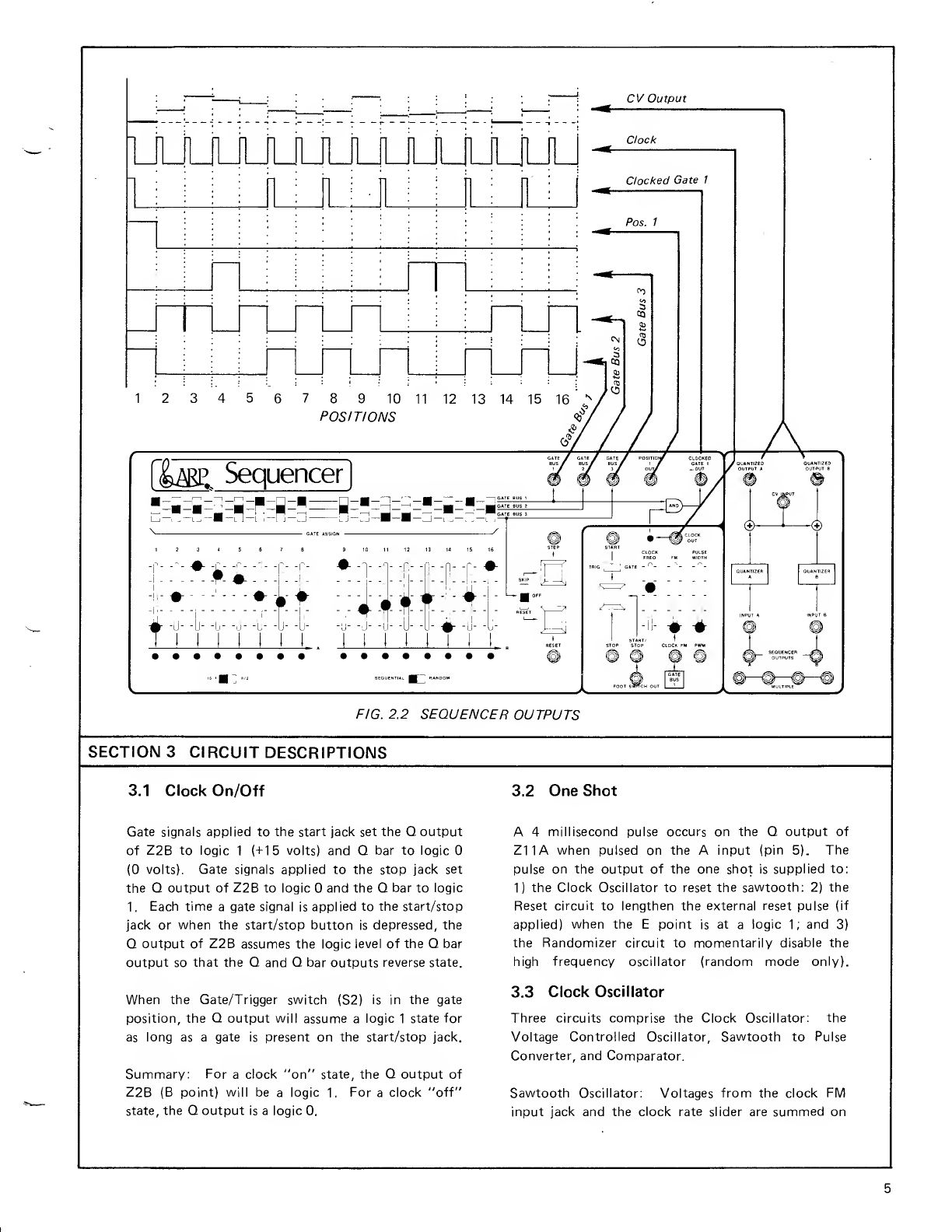
3.4 Randomizer, Skip &Reset
Z1 1Bis ahigh speed oscillator (approx. 5 microsec).
When Z16A pin 3is alogic 1,Z1 1Bproduces ahigh
frequency pulse chain on pin 9. When Z16Z pin 3is
at alogic (ground) Z11B stops oscillating. With
slide switch S21 in the Random position, Z10C pin
10 will enable (turn on) the high speed oscillator
(Z11B) through Z16A. Z11B will then provide a
pulse chain to Mask circuit. When pulsed by the
clock oscillator, the one shot will momentarily turn
off the high speed oscillator through Z10C (pin 12 &
13) to allow the latch in the Counter/Latch circuit to
memorize a(random) position. During this mode,
Z7B generates random voltage levels to vary the fre-
quency of Z11B to insure arandom sampling of
positions. With S21 in the Sequential mode, Z10C
will not affect the frequency of the high speed
oscillator. When S22 is in the skip position, pin 8
of Z9C is at logic 0. When the Jpoint is also at a
logic 0, Z9C pin 10 then turns on the high speed
oscillator which quickly advances the sequencer
to the next position (via Z16C).
In the reset position, the gate signal on the Jpoint
is supplied through S22 to Z9D. When the Jpoint
is at logic 0, Z9D supplies alogic 1which resets the
counter to position 1via Z16B. External reset gates
may be applied to Q27 and by depressing the reset
push button (S23).
3.5 Mask Circuit
Z15A pin 3is logic 1when the sequencer is in the
"sequential" mode which allows the latch (Z8) in
the Counter/Latch circuit to transmit data con-
tinuously. When pin 3of Z15A is logic 0, (random
mode only) Z8 in the Counter/Latch circuit holds or
stores the data on the counter output.
The one shot pulse will cause the Qand Qbar out-
puts of Z2A to momentarily reverse state. The
output of the high speed oscillator (Z11B) and the
Qbar output of Z2A are then combined on Z16C
which advances the counter in the Counter/Latch
circuit. A"mask" pulse is generated by combining
the one shot pulse (4 msec, duration) and the pulse
from Z2A (8 microsec. duration) on the output of
Z15B (pin 4) to turn off all the gate outputs during
the time the counter is advanced from one position
to the next.
3.6 Step
When gate signals are applied to the step jack or from
the step push button, Z6A pin 3provides apulse to
the One Shot circuit and the Gate Output Processing
circuit.
3.7 Foot Switch Jack
The foot switch jack on the front panel provides a
+10 volts gate for as long as the foot switch is held
and can be patched to any of the input jacks on the
front panel.
3.8 Counter/Latch
Z7A is adivide by 16 counter providing a4bit code
to Z8. Z8 is alatch circuit but normally transmits
data to the Decoder circuit unaffected. Z9B and Z9A
are connected to the Qand Qbar outputs of Z8 to
enable Z13 and Z14 in the Decoder circuit one at a
time (sequentially).
3.9 Decoder
Z13 and Z14 decode the binary number from the
Latch circuit to one of 16 positions. When S4B is in
the 16 X1mode, Q1 1through 26 will turn on one at
atime sequentially (1 through 16). In the 8X2
mode, Z13 and Z14 decode in parallel (position
1-8 and 9-16). In the random mode, the counter
advances at the rate of the High Speed Oscillator
(Z11B, schematic 1) but in this mode, Z8 holds
the code which is supplied to the decoders constant.
The strobe input of the Z8 allows arandom binary
number to be memorized on each clock pulse which
is supplied to the decoder.
Q1 1and Q26 are turned on one at atime and supply
voltages to one of the three gate bus lines through the
three position gate switches. At the same time, the
LED is lit indicating which position is on. The three
position slide switches provide the path to ground
for the LEDs.