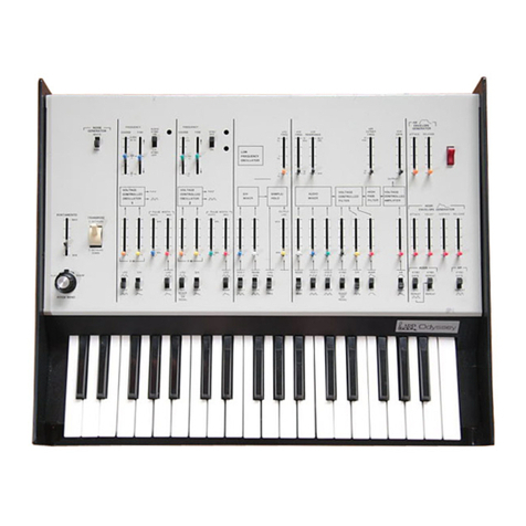
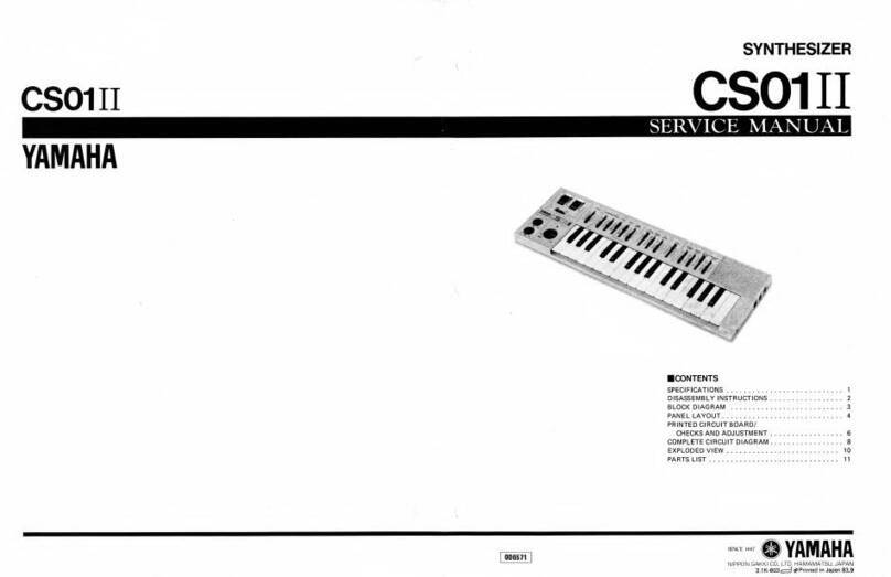
ARP ODYSSEY User manual

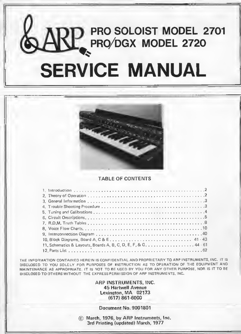
ARPODYSSEY
SERVICE
MANUAL
MODELS
2800
THROUGH
2823

SECTION
1
1.1
Introduction
This
service
manual
is
divided
into
three
major
sections:
А)
Circuit
Descriptions,
B)
Trim
Pro-
cedures,
and
C)
Board
Test
Points.
The
circuit
descriptions
should
be
consulted
when
a
problem
is
suspected
in
a
particular
area
of
the
instrument.
The
trim
procedures
should
be
used
to
verify
cali-
brations
or
when
a
component
has
been
changed.
The
board
test
points
are
a
quick
reference
to
verify
circuits
with
suspected
problems
and
should
be
checked
whenever
a
problem
has
been
identified.
1.2
Board
Identification
Three
types
of
Odyssey
models
have
been
produced:
1)
2800,
2)
2810-2815
апа
3)
2820-2823.
The
model
and
serial
number
are
located
at
the
rear
or
bottom
of
the
Odyssey
chassis.
Except
for
2800,
a
typical
number
might
read:
2813-0490.
For
model
2800,
the
first
two
digits
of
the
serial
number
denote
the
model,
such
as:
28490.
Listed
below
are
the
board
identification
numbers
for
each
model;
they
will
be
referenced
in
the
service
manual
by
model
number
for
easy
identification.
ODYSSEY-|
Model
2800
Board:
A-1
B-1
C-1
PWR
SUP-1
ODYSSEY-II
Model
2810-2813
Model
2820-2823
Board:
A-II
Board:
A-IH
(with
PPC)
B-II B-II
C-I
С-ІІ
PWR
5ОР-ІІ
PWR
5ОР-ІІ
Note:
Some
Odyssey-2
models
employ
the
older
style
Board
В-І.
1.3
Model
Changes
The
Odyssey
has
undergone
major
cosmetic
and
electrical
changes
since
its
original
production
in
1972,
however,
the
functional
capabilities
have
remained
virtually
unchanged.
The
following
are
the
most
noticeable
physical
differences
among
models:
PRELIMINARY
INFORMATION
MODEL
2800
Black
and
white
face
panel
(some
later
models
have
black
and
gold
face
panels).
Pitch
Bend
knob
No
Factory
installed
interface
jacks.
Wrap
around
vinyl
bottom
cover.
MODEL
2810-2813
Black
and
gold
face
panel.
New
style
power
switch.
Factory
installed
interface
jacks:
Pitch
Bend
knob.
(Some
later
models
have
PPC.)
Wrap
around
vinyl
bottom
cover.
MODEL
2820-2823
(current
model,
Odyssey
'78)
Black
and
orange
face
panel:
Steel
chassis
Leather
endblocks
PPC
The
major
electrical
changes
found
in
the
Odyssey-ll
ὁ
as
compared
to
the
Odyssey-l
are:
1.
Uses
24db/octave
filter
in
place
of
12db/
octave.
2.
Improved
VCO
design
for
better
tracking;
and
stability.
3.
Improved
power
supply
regulation.
4.
Improved
keyboard
current
source
for
CV
generation.
5.
Improved
S/H
memory
circuit
design.
1.4
Revisions/Changes
1.4.1
MODIFICATION
KITS
The
following
modifications
are
available
from
the
Factory
for
updating
older
style
Odysseys:
Modification
For
Model
Kit
No.
Interface
Jacks
2800
6800101
PPC
2810-2815
6800301
PPC
2800
6800501
1.4.2
KEYBOARD
CONVERSION
The
Odyssey-ll
is
designed
to
be
used
with
а
two
bus
keyboard.
When
an
Odyssey-ll
is
used
with
a
three
bus
keyboard,
an
interface
board
is
inserted
on
the
molex
pins
on
Board
Α-ἱ
to
make
the
keyboard
compatible
with
the
electronics.
Illustrated
below

are
the
two
types
of
keyboards
employed
in
the
Odyssey
and
their
schematics.
TWO
BUS
KEYBOARD
Models
2810-2813
(Later
models
use
cat-whisker
style
shown
in
maintenance
section
6.2.
Schematic
remains
the
same.)
KYBD
LO
4
99
DY,
is
“а
KYBD
HI
cv
Bus
مد
دي
E
NL
GATE
BUS
GROUND
Р\-\
О
GATE
м
WEYS
085
e$
KEYS
төбе
$
IN
1.4.3
TYPES
OF
VOLTAGE
CONTROLLED
FILTERS
The
4023
voltage
controlled
filter
is
no
longer
avail-
able
from
the
Factory.
Instead,
the
newer
4075
filter
can
be
used
to
replace
the
4023
with
the
following
modification
(see
Field
Change
Notice
007):
The
earlier
model
Odyssey-lls
used
a
4035
voltage
controlled
filter,
which
has
since
then
been
replaced
by
the
4075.
Мо
modifications
are
necessary
when
replacing
a
4035
filter
with
a
4075.
"THREE
BUS
KEYBOARD
GATE
TRIGGER
ον
KYBD
LO
KYBD
HI
M
cv
sus
اا
4
+15
8
XX
=
1
GROUND
267
\
IIl
5
е
7
——
O
TRIG
BUS
#———
О
GATE
BUS
r
<
ш
з
v
a
°
е
9
5
a
ІМІЕНЬУСЕ
ВО"
VIOLET
A
change
R1,2,&
3
to
680K
Change
T4
to
100
ohm
trimmer
Ж
=
Break
connection

1.4.4
NOISE
MODIFICATION
The
newer
style
Odysseys
use
a
zener
diode
as
a
noise
source
instead
of
a
noise
transistor.
Defective
noise
transistors
can
be
replaced
with
a
zener
diode,
pro-
vided
the
following
circuit
modification
is
performed:
Zener
diodes
tend
to
produce
a
greater
spectrum
of
white
noise
with
little
or
no
noise
break-up.
1.9
Specifications
Noise
Generator
Noise
spectrum
types:
White
and
Pink
Voltage
Controlled
Oscillators
Waveforms:
Sawtooth,
Square,
Pulse,
Dynamic
Pulse
Frequency
range:
VCO
1
іп
low
freq.
mode,
.2
Hz
to
20
Hz;
VCO
1
and
VCO
2
(audio
range),
20
Hz
to
20
KHz
Warm
up
drift:
1/30
semitone
from
turn
on
max.
Pulse
width:
5096
to
596
Pulse
width
modulation:
ADSR,
+45%;
ГЕО,
+15%
Voltage
controlled
response:
1V/oct.
Maximum
frequency
shifts:
LFO
sine
wave,
+1⁄2
oct.;
LFO
square
wave,
+1.5
oct.;
ADSR
+9oct.;
S/H
*2
oct.
Note:
VCO
1
is
a
low
note
priority;
VCO
2
is
high
note
priority
Transpose
Positions:
Down
2
octaves,
normal,
up
2
octaves
Pitch
Bend
Frequency
shift:
About
+
1
oct.
(exactly
1
octave
on
Odyssey-2)
PPC
Frequency
shift:
About
5
semitones
+1
semitone.
Portamento
.
Maximum
speed:
About
.01
msec./oct.
Minimum
speed:
About
1.5
seconds/oct.
Ring
Modulator
Type:
Digital
Input
signals:
VCO
1
and
VCO
2
pulse
waves
ud
REMOVE
|
O.O
гмеоте
Cn
ws
Voltage
Controlled
Filter
Type:
Low
pass
Frequency
range:
16
Hz
to
16
KHz
Maximum
usable
Q:
30
Resonance
1⁄2
to
self
oscillate
Voltage
controlled
response:
1V/oct.
Voltage
Controlled
Amplifier
Dynamic
Range:
80dB
Sample
and
Hold
Command
sources:
Sampled
signals:
VCO
1
square
wave
and
sawtooth
wave,
VCO
2
square
wave
and
pink
noise
Keyboard
or
LFO
trigger
ADSR
Envelope
Generator
Attack
time:
5
msec.
to
5
seconds
Decay
time:
10
msec.
to
8
seconds
Sustain
level:
O
to
10096
of
peak
Release
time:
15
msec.
to
10
seconds
AR
Envelope
Generator
Attack
time:
5
msec.
to
5
seconds
Release
time:
10
msec.
to
8
seconds
Audio
Outputs
High
level:
2.5VPP
max.;
100K
impedance
Low
level:
.25VPP
max.;
10K
impedance
Interface
Jacks
Keyboard
CV
IN/OUT:
1V/oct.
Gate
OUT:
+10V,
key
down;
OV
all
keys
up
Gate
IN:
+8V
minimum
Trigger
OUT:
+10\/
pulse
on
key
depression,
10
microsec.
duration
Trigger
IN:
+8V
pulse
min.,
10
microsec.
duration
minimum
External
Audio
Input:
500
millivolts
for
full
output

9)
Front
and
Back
Panel
Configuration
Model
2823
HC
19:9
“а
ΗΟ)
£
з
T3
іе
i
ASSEMBLY/DISSASSEMBLY
MODEL
2800
:
2815
MODEL
2820
-
2823
Ф
NOTE:
These
two
screws
MUST
be
replaced
in
ые
`
|
КЕУВОАВО
REMOVAL
KEYBOARD
REMOVAL

Andino
aman
мем
І
andino
“ала
we
[
Ф
Atc!
Qoy
1».
бечоб
везчычч
си
21940
(м-
255142)
ADAM
509
7
шелбега
зогицоолаци|
(г
9
|
AessApO)
0082
ΙϑΡΟΙΛ

TWOLLJ3fTNO)
HOUMS
QAW3S
Q8
2d
«65м
Š
3
в
южюгь
:
WI
10470
ғыр
3345"
ΜΟΊ
28437
WH
IO"
o2L
Ф965
з
ты
HOUMS
жоі
1004
1804
ае,
шее
πα
тө
Sie
11/1
ти
зі
Lis
LL/
190
319
Gre
stern
κ
vo)
ам
«|
мому
IOL'C2L
змов
Эа
NOWIANNOD
aan!
шелбега
зогицоолади|
£Z8Z
-
0282
I9POIA
SNIMVAG
40
меч
WOLOS
335
NOIDINNOD
HILIMS
Όλνί3ς
ысы
εοοιζοι,
531835
7
SSN
2'смучОёлхая
2051251
Assy
захо

SECTION
2
CIRCUIT
DESCRIPTIONS
(Board
А-1)
2.1.1
Trigger
Circuit
Each
key
on
the
keyboard
has
its
own
capacitor-
resistor-diode
network.
The
capacitors
are
normally
charged
to
+15
volts
until
a
key
is
depressed
at
which
time
the
capacitor
discharges
through
the
diode
creating
a
trigger
pulse
on
the
trigger
bus
rod.
Q1
through
O4
are
a
monostable
multivibrator
which
delays
the
trigger
pulses
15
milliseconds
to
allow
the
gate
and
CV
to
stabilize.
2.1.2
PITCH
BEND
P1,
the
pitch
bend
control,
supplies
a
control
voltage
to
both
VCOs
on
Board
B.
CR4
and
СНБ
create
a
'dead'
zone
when
the
control
is
centered.
2.1.3.
CURRENT
SOURCE
Q5
supplies
constant
current
to
a
resistor
divider
chain
made
up
of
thirty-six
100
ohm
resistors
con-
nected
in
series,
The
CV
contacts
are
located
at
the
junction
of
each
of
the
100
ohm
resistors
to
supply
a
specific
voltage
to
the
contro!
voltage
memory
when
a
key
is
depressed.
There
is
a
three
volt
drop
across
the
entire
resistor
chain,
or
one
volt
per
octave.
T1,
the
Volts/Octave
trimmer,
adjusts
the
current
through
the
resistor
chain
to
produce
the
correct
voltage
drop
across
the
keyboard.
2.1.4.
TRANSPOSE
SWITCH
Half
of
the
transpose
switch
is
connected
to
the
bottom
end
of
the
resistor
chain
to,
in
effect,
add
two
or
four
octaves
worth
of
resistance
(about
1200
or
2400
ohms)
to
the
resistor
chain.
This
raises
the
control
voltage
level
supplied
to
the
CV
memory.
The
following
chart
summarizes
the
CV
output
for
low
'C'
and
high
'C'
on
the
keyboard
for
each
of
the
transpose
switch
positions:
TRANSPOSE
SWITCH:
DOWN
2
OCT.
NORMAL
UP
2
OCT.
The
remaining
half
of
the
transpose
switch
com-
pensates
the
second
voice
control
voltage
for
the
difference
in
the
resistor
chain
resistance.
2.1.5
CV
Memory
Circuit
Об
апа
АЛА
are
a
FET
input
op
amp
which
buffers
the
voltage
from
the
keyboard
CV
bus
and
supplies
it
to
the
memory
circuit
through
R23
and
CR3.
When
a
key
is
depressed,
+15
volts
is
supplied
from
the
keyboard
gate
through
CR2
and
R21
which
reverse
biases
CR3
and
allows
Q7
to
conduct.
The
control
voltage
from
A1A
is
then
allowed
to
charge
the
memory
capacitor,
C8.
When
a
key
is
released,
Q7
turns
off
to
prevent
СВ
from
discharging.
О8
and
A1B
are
a
FET
op
amp
which
buffers
the
control
voltage
on
C8
and
supplies
it
to
the
control
input
of
VCO
1
and
VCO
2
on
Board
B
and
to
the
VCF
on
Board
C.
2.1.6
Second
Voice
CV
Generator
When
two
or
more
keys
are
depressed,
a
section
of
the
resistor
chain
is
effectively
shorted
out
which
drops
the
voltage
at
the
top
end
of
the
resistor
chain.
This
voltage
drop
corresponds
to
the
‘voltage
dif-
ference’
between
two
held
keys.
A2A
is
a
unity
gain
buffer
which
monitors
the
voltage
at
the
top
of
the
resistor
chain
and
supplies
it
to
A2B.
A2B
sums
the
voltage
from
А2А
with
the
voltage
supplied
by
R31
and
R30.
These
resistors
are
selected
to
produce
zero
volts
on
the
output
of
A2B
when
either
no
keys
or
one
key
is
depressed.
When
two
or
more
keys
are
depressed,
the
voltage
at
the
top
end
of
the
resistor
chain
drops,
which,
in
turn,
decreases
the
voltage
supplied
to
228.
228
then
supplies
the
difference
voltage
to
the
control
input
of
VCO
2
where
it is
summed
with
the
control
voltage
from
the
CV
memory
circuit.
This
summation
allows
VCO
2
to
be
controlled
by
the
highest
key
depressed.
Since
VCO
1
is
fed the
con-
trol
voltage
from
the
CV
memory
only,
its
pitch
is
controlled
by
the
lowest
key
depressed.
2.1.7
Noise
Generator
The
noise
generator
circuit
produces
10VPP
white
and
pink
noise
signals
which
are
supplied
to
the
VCF
audio
input
and
the
S/H
mixer.
The
noise
is
obtained
by
amplifying
a
reversed
biased
transistor
junction
(Q9)
in
avalanche
breakdown.
Q9
is
a
transistor
selected
for
optimum
avalanche
characteristics;
and
therefore,
has
good
noise
producing
capability.
A3
amplifies
and
clips
the
noise
signal.
АЗ
filters
the
noise
to
provide
pink
noise
to
the
VCF
and
S/H.

CIRCUIT
DESCRIPTIONS
(Board
B-
1)
2.2.1
Sample
&
Hold
(S/H)
The
sample
and
hold
circuit
provides
a
DC
voltage
output
by
sampling
and
storing
the
instantaneous
voltage
level
of
signals
on
its
input
each time
a
trigger
pulse
is
provided.
This
stored
voltage
is
held
until
the
next
trigger
pulse
occurs.
Signals
which
are
to
be
sampled
and
applied
to
pin
3
of
A3.
A3
is
an
op-
erational
transconductance
amplifier
(OTA),
which
is
used
as
a
gated
voltage
follower:
when
a
pulse
is
applied
to
pin
5
of
Z3,
capacitor
C7
charges
to
the
voltage
level
on
pin
3.
This
voltage
level
is
held
until
another
pulse
is
applied
to
pin
5.
ОЗ
buffers
the
voltage
on
C7
and
supplies
it
to
A2B
through
the
lag
slider
(P16).
A2B
is
a
unity
gain
buffer.
The
sample
and
hold
output
is
supplied
to
the
control
inputs
of
VCO
1
and
УСО2
and
to
the
УСЕ
on
Board
С.
2.2.2
Low
Frequency
Oscillator
(LFO)
The
LFO
produces
a
triangle
and
square
wave
output
in
a
frequency
range
from
about
.1
Hz
to
25
Hz.
Z1A
and
C3
are
an
integrator
which
charges
from
current
passing
through
R11.
218
is
а
hysteretic
switch
whose
output
switches
from
-15
volts
to
+15
volts
when
the
output
of
Z1A
reaches
+5
volts.
This
then
reverses
the
direction
of
current
through
R11
and
the
rate
control
(Z5)
and
thus
the
direction
of
integration
at
the
output
of
Z1A.
When
the
output
of
Z1A
reaches
-5
volts,
the
output
of
Z1B
switches
back
to
-15
volts
and
the
cycle
repeats.
An
LFO
reset
pulse
is
supplied
from
the
keyboard
every
time
a
key
is
depressed.
O1
and
Q2
are
turned
on
momentarily
by
the
keyboard
trigger
pulse
to
discharge
the
integrating
capacitor
(C3)
thus
reini-
tializing
the
LFO
to
zero.
2.2.3
Voltage
Controlled
Oscillators
(VCO)
Oscillator
circuit
(VCO
1
&
2):
Control
voltages
from
the
keyboard,
initial
frequency
and
fine
tune
sliders,
pitch
bend
(2800
only)
and
both
FM
input
sliders
are
summed
on
the
base
of
O4.
O4
and
Q5
are
a
linear
voltage
to
exponential
current
generator;
for
every
volt
applied
from
the
keyboard,
the
current
through
Q5
will
double.
C12
is
the
integrating
capacitor;
it
is
initially
charged
to
+15
volts
and
discharges
through
R51
and
Q5
toward
ground.
Q5
determines
the
discharge
time
of
the
capacitor
and
therefore
the
period
of
oscillation.
Z1D
is
a
CMOS
nand
gate
used
as
a
comparator.
When
the
voltage
on
pin
12
of
210
falls
below
“7,5
volts,
the
output
of
Z1
(pin
11)
changes
from
zero
volts
to
+15
volts
which
turns
on
Q10,
О7
and
Об.
Об
recharges
the
integrating
capacitor
(C12)
to
+15
volts
to
start
the
cycle
over
again.
Q8
buffers
the
sawtooth
wave
on
C12
and
supplies
it
to
the
sawtooth
to
pulse
converter
and
09,
the
output
emitter
follower.
The
oscillator
circuit
for
VCO
2
is
the
same
as
VCO
1.
When
the
‘SYNC’
switch
is
on,
the
reset
pulse
from
VCO
1
is
applied
to
Z2D
which
causes
VCO
2
to
reset
at
the
same
time
as
VCO
1,
regardless
of
the
voltage
level
on
pin
12
of
Z2D.
The
waveform
on
the
output
of
VCO
2
is
then
synchronized
with
VCO
1.
Sawtooth
to
square
wave
converter:
Z1A
and
Z1B
are
a
R-S
flip-flop
with
pin
8
used
as
a
comparator.
The
reset
pulse
from
Z1C
is
supplied
to
pin
1
and
the
sawtooth
wave
to
pin
8.
Аз
the
sawtooth
wave
is
raised
above
the
zero
reference
by
the
pulse
width
trimmer
and
sliders
(T2,
P8
and
P9)
the
flip-flop
will
change
state
on
a
different
point
of
the
sawtooth
slope
resulting
in
a
different
pulse
width.
With
all
of
the
pulse
width
sliders
on
the
front
panel
at
mini-
mum,
the
pulse
wave
should
be
square
(5096
duty
cycle).
The
pulse
wave
output
is
supplied
to
the
audio
input
of
the
VCF
on
Board
C
and
to
the
ring
modulator
circuit
on
Board
B.
2.2.4
Ring
Modulator
The
ring
modulator
utilizes
two
CMOS
nand
gates
(218
and
228)
and
O18
in
an
exclusive
‘or’
functior.
Square
waves
from
VCO
1
and
VCO
2
are
supplied
to
pin
5
of
Z1
and
Z2
and
the
output
is
taken
from
the
emitter
of
O18.
GATE
TRUTH
TABLES
AND
GATE
B
C
XCLUSIVE
OR
VCO
2
|
|
ΠΗΓΗ
ΠῚ
RING
MODULATOR
OUTPUT

2.3.1
Voltage
Controlled
Filter
(УСЕ)
Audio
signals
from
both
VCOs,
the
ring
modulator,
and
the
noise
generator
are
applied
to
the
audio
input
of
the
voltage
controlled
filter
(pin
1,
4023)
through
C1.
Control
voltage
from
the
S/H,
LFO,
KYBD
CV,
and
the
envelope
generators
are
summed
and
inverted
by
А1.
The
control
input
of
the
МСЕ
accepts
negative
going
control
voltages;
as
the
voltage
on
pin
3
of
the
4023
module
is
decreased,
the
filter
cutoff
increases.
Signals
on
the
output
of
the
VCF
(pin
10)
are
fed
back
to
the
resonance
input
(pin
2)
via
the
resonance
slider,
(P2).
2.3.2
Voltage
Controlled
Amplifier
(VCA)
Audio
signals
from
the
VCF
are
processed
through
the
high
pass
filter
(C3,
R13
and
P3)
and
connected
to
the
noninverting
input
of
A3.
A3
is
an
operational
transconductance
amplifier
(OTA)
whose
gain
is
a
function
of
the
current
supplied
to
pin
5.
Control
voltages
from
the
two
envelope
generators
and
the
УСА
gain
slider
are
connected
to
Q1
which
supplies
current
to
the
OTA.
T2,
the
control
reject
trimmer,
balances
the
inputs
of
the
OTA
to
minimize
the
effect
of
control
voltages
on
the
audio
output
of
the
VCA.
2.3.3
AR
Envelope
Generator
The
Attack-Release
envelope
generator
produces
a
control
voltage
with
variable
rise
and
fall
times.
Itis
used
to
control
the
VCF
or
the
VCA.
When
a
gate
voltage
is
supplied
by
the
keyboard
or
the
LFO
through
510,
Q4
turns
on
which
charges
capacitor
C7
through
P5,
R32
and
CR5.
The
position
of
P5
(Attack
Slider)
determines
the
time
C7
takes
to
charge
up.
When
the
gate
voltage
is
removed,
Q4
turns
off
which
allows
Q5
to
turn
on.
The
voltage
on
C7
then
discharges
through
CR6,
P6,
R31,
and Q5.
P6
(Release
slider)
sets
the
release
time.
Q6
and
Q7
buffer
the
voltage
on
C7
and
supply
it
to
the
VCA
and
VCF.
2.3.4
ADSR
Envelope
Generator
The
Attack-Decay-Sustain-Release
envelope
generator
produces
a
control
voltage
with
variable
rise
and
fall
times.
It
is
used
to
control
the
VCF
or
the
VCA
and
a
gate
and
trigger
signal
must
be
supplied
from
the
keyboard
or
LFO
to
start
the
ADSR
voltage
rising.
Attack:
When
a
gate
signal
(+10
volts)
is
supplied
through
S8,
Q8,
09
and
010
turn
on
which
then
allows
O16
to
turn
off.
With
Q16
off,
a
trigger
applied
through
C9
and
R55
will
momentarily
turn
CIRCUIT
DESCRIPTIONS
(Board
C-
1)
TRIGGER
ATTACK
LI
AR
OUTPUT
ADSR
OUTPUT
SUSTAIN
KEY
DOWN
NOTE:
The
ADSR
is
initiated
with
a
gate
and
trigger
volt-
age,
and
the
AR
envelope
requires
only
the
gate.
оп
О18
and
017.
017
then
supplies
+15
volts
through
CR18,
CR19,
CR17
and
R57
to
hold
Q18
on.
018
and
017
(the
attack
latch)
now
supplies
+15
volts
through
the
attack
slider
(P4),
R43,
and
CR9
and
charges
up
the
integrating
capacitor,
C8.
012,
013,
and
014
buffer
the
voltage
оп
C8
апа
provides
it
to
the
VCA
and
МСЕ.
Q15
is
the
peak
detector
which
monitors
the
output
of
the
ADSR.
When
the
ADSR
voltage
reaches
its
maximum,
(about
*10
volts),
Q15
will
turn
on
and
provide
this
voltage
to
the
base
ої
Q16
through
CR15.
016
then
grounds
out
the
voltage
on
the
base
of
018
to
unlatch
018
and
Q17
and
end
the
attack
portion
of
the
ADSR
cycle.
Decay
&
Sustain:
When
the
attack
portion
of
the
ADSR
cycle
has
completed,
the
voltage
on
C8
is
allowed
to
discharge
through
CR11,
R47,
and
the
decay
slider
(P15)
to
the
emitter
of
Q11.
The
sustain
slider
(P16)
sets
the
voltage
level
on
the
base
of
O11.
When
the
voltage
level
on
the
emitter
of
O11
falls
below
the
level
on
the
base,
Q11
turns
off
and
prevents
the
voltage
on
O8
from
discharging
further.
Release:
When
the
gate
is
removed,
the
remaining
voltage
оп
C8
is
discharged
to
ground
through
CR
10,
R44
and
the
release
slider
(P17).

CIRCUIT
DESCRIPTIONS
(Board
А-11)
2.4.1
Keyboard
Current
Source
The
keyboard
current
source
supplies
constant
current
through
thirty-six
100
ohm
resistors
con-
nected
in
series.
These
resistors
are
a
voltage
divider
supplying
specific
voltages
for
each
key
on
the
key-
board.
The
top
end
of
the
resistor
chain
is
connected
to
J2-5
and
the
low
end
to
J2-6.
The
current
source
produces
a
3
volt
drop
across
the
entire
keyboard,
or
1
volt
per
octave.
The
keyboard
voltage
is
fed
to
the
CV
memory
via
the
CV
bus
rod.
Pin
7
of
Z2A
(high
end
of
the
resistor
chain)
is
O
volts
when
either
no
keys
or
one
key
is
depressed
and
pin
6
of
Z2A
(low
end
of
the
resistor
chain)
is
+3
volts.
When
two
keys
are
depressed,
the
contacts
and
bus
rod
short
out
a
section
of
the
resistors
in
the
divider
chain
which
reduces
the
gain
of
Z1A
thereby
raising
the
voltage
оп
Z2A
pin
7.
This
voltage
increase
represents
the
voltage
difference
between
two
held
keys.
When
this
difference
voltage
is
sub-
sequently
added
to
the
control
voltage
at
the
control
input
of
VCO
2
(Bd.
B),
high
note
priority
control
over
the
pitch
of
VCO
2
is
produced.
2.4.2
Control
Voltage
Memory
Control
voltages
supplied
from
the
keyboard
CV
bus
are
buffered
by
a
unity
gain
amplifier,
Z4A.
This
voltage
is
then
supplied
to
the
memory
capacitor
C8
through
the
portamento
slider
(R30)
and
the
gating
FET
(Q3).
ОЗ
is
turned
on
by
the
gate
generator
circuit
only
while
a
key
is
depressed.
O4
and
Z4B
are
a
FET
follower
with
high
input
impedance
to
buffer
the
voltage
on
capacitor
C8.
J3-1
and
J3-2
аге
connected
to
the
portamento
footswitch
jack
so
that
the
portamento
slider
can
be
bypassed
while
the
foot-
switch
is
plugged
in.
2.4.3
Pitch
Bend
Pitch
Bend:
The
Pitch
Bend
control
supplies
an
off-
set
voltage
to
Z2B
to
be
summed
with
the
control
voltage
from
Z4B
(CV
memory).
СВЗ
and
CR4
create
a
'dead'
zone
when
the
control
is
centered
and
R27
calibrates
the
output
to
exactly
plus
and
minus
a
volt.
2.4.4
PPC
The
PPC
circuit
contains
three
resistive
carbon
strips,
three
conductive
rubber
strips
and
various
summing
resistors.
Each
end
of
the
carbon
strip
is
connected
to
a
designated
voltage
source,
while
each
end
of
the
conductive
rubber
is
making
contact
with
the
sum-
ming
resistors.
As
the
PPC
button
is
depressed,
the
conductive
rubber
makes
contact
at
various
points
on
the
carbon
strip
which,
in
turn,
provides
various
degrees
of
control
voltage
to
the
summing
resistors.
The
conductive
rubber
is
tapered
so
that
maximum
sensitivity
is
achieved
at
the
top
of
the
button.
2.4.5
Transpose
Switch
Transpose:
The
transpose
switch
also
supplies
an
offset
voltage
to
Z2B
to
be
summed
with
the
control
voltage
from
Z4B.
R23
calibrates
the
output
to
exactly
plus
and
minus
2
volts.
246
Summing
Circuit
Summing:
The
output
of
Z4B
is
+3
volts
when
high
"С"
is
depressed
апа
0
volts
when
low
"С"
is
depressed.
This
control
voltage
is
summed
with
the
offset
voltages
from
the
transpose
and
pitch
bend
circuits
on
the
input
of
Z2B.
72В
is
a
unity
gain
inverter
whose
output
will
be
0
volts
with
low
"С"
depressed
(pitch
bend
and
transpose
in
the
normal
position)
and
+3
volts
with
high
‘C’
depressed.
This
voltage
is
supplied
to
the
VCOs
on
Board
B
(pitch
control)
and
the
VCF
on
Board
C
(filter
cutoff
control).
2.4.7
Gate
Generator
Each
gate
contact
on
the
keyboard
is
connected
to
a
2.2K
ohm
resistor
to
ground.
When
a
key
is
de-
pressed
the
gate
bus
voltage
drops
from
+15
volts
to
about
+10
volts
which
turns
on
Q1.
Q1
supplies
two
gate
signals:
SIGNAL:
CV
Memory
-15V
+15
М
Key
up:
Key
down:
Location:
Q1
coll.
Gate
out
ом
з10
М
J4-3
+15
V
GATE
BUS
VOLTAGE
+10
V
;
H
+8
V
4
Key
down
Second
key
down
LAU
keys
up
| |
TRIGGER
OUTPUT
2.4.8
Trigger
Generator
When
a
key
is
depressed,
the
gate
bus
voltage
drops
from
+15
volts
to
about
+10
volts.
Additional
key
depressions
will
drop
this
voltage
still
further.
These
voltage
transitions
are
coupled
through
capacitor
C1
and
R4
to
02.
Capacitor
C2
is
charged
to
*15
volts
by
Q2
when
a
key
is
depressed.
21С
апа
210
are
CMOS
папа
gates
(threshold
is
+7.5
volts).
As
C2

charges
up,
210
pin
11
will
produce
a
10
millisecond
pulse
(the
pulse
width
is
determined
by
C2)
which
is
supplied
to
Q8.
О8
will
conduct
during
the
fall
of
the
pulse
from
Z1D
to
provide
a
+10
volt
trigger
pulse
(20
microsecond
duration)
to
Board
C
and
B.
Trigger
pulses
from
external
sources
are
coupled
through
C20,
21А
and
Z1B
to
O8.
Z1A
and
218
are
connected
in
parallel
to
increase
drive.
2.4.9
Noise
Generator
The
noise
generator
circuit
produces
10VPP
white
and
pink
noise
signals
which
are
supplied
to
the
VCF
audio
input
and
the
S/H
mixer.
The
noise
is
obtained
by
amplifying
a
reversed
biased
transistor
junction
(ОБ)
in
avalanche
break
down.
ОБ
is
a
transistor
selected
for
optimum
avalanche
characteristics
and
therefore
has
good
noise
producing
capability.
Об
is
a
buffer
and
25
amplifies
and
clips
the
noise
signal.
Z3
filters
the
noise
to
provide
pink
noise
to
the
VCF
and
S/H.
NOTE:
The
more
recent
model
Odysseys
employ
a
zener
diode
instead
of
a
noise
transistor.
See
the
re-
visions
section
1.4.4
for
the
circuit
change.
CIRCUIT
DESCRIPTIONS
(Board
B-II)
2.5.1
Sample
δι
Hold
(S/H)
The
sample
and
hold
circuit
provides
a
DC
voltage
output
by
sampling
and
storing
the
instantaneous
voltage
level
of
signals
on
its
input
each time
a
trigger
pulse
is
provided.
This
stored
voltage
is
held
until
the
next
trigger
pulse
occurs.
Signals
which
are
to
be
sampled
are
applied
to
pin
3
of
Z1A.
Z1A
amplifies
and
buffers
the
signal
and
supplies
it
to
O1.
When
a
trigger
from
either
the
LFO
or
the
keyboard
is
received
through
СЗ,
О1
conducts
just
long
enough
for
the
memory
capacitor
(C1)
to
assume
the
new
voltage
level.
Then
O1
turns
off
until
another
trigger
is
supplied.
02
and
22А
аге
а
FET
op
amp
follower
which
buffers
the
voltage
on
C1
and
provides
it
to
the
lag
circuit
(R15
and
C2)
and
the
output
buffer
(Z2B).
Noise
Generator
LFO
Trigger
(LFO
Trig.
off)
———_h
b
S/H
Output
2.5.2
Low
Frequency
Oscillator
(LFO)
The
LFO
produces
a
triangle
and
a
square
wave
out-
put
in
a
frequency
range
from
about
.1
Hz
to
25
Hz.
25А
and
C7
are
ап
integrator
which
charges
from
cur-
rent
passing
through
R33.
Z5B
із
а
hysteretic
switch
whose
output
switches
from
-15
volts
to
+15
volts
when
the
output
of
Z5A
reaches
+5
volts.
This
change
in
output
polarity
then
reverses
the
direction
of
current
through
R33
and
the
rate
control
(R34)
and
thus
the
direction
of
integration
of
the
output
ої
ZbA.
When
the
output
of
Z5A
reaches
-5
volts,
the
output
of
Z5B
switches
back
to
-15
volts
and
the
cycle
repeats.
An
LFO
reset
pulse
is
supplied
from
04
every
time
a
key
is
depressed.
ОБ
is
turned
on
momentarily
by
the
LFO
reset
pulse
and
discharges
the
integrating
capacitor
(C7)
thus
reinitializing
the
LFO
output
to
zero.
2.5.3
Voltage
Controlled
Oscillators
(VCO)
Control
voltages
from
the
keyboard,
initial
fre-
quency
and
fine
tune
sliders,
the
sample
and
hold
circuit,
LFO
square
wave
and
sine
wave,
and
the
ADSR
are
summed
on
the
base
of
Q6.
Q6
and
O7
are
a
linear
voltage
to
exponential
current
generator;
for
every
volt
applied
to
the
control
input
of
the
VCO
from
the
keyboard,
Q6
will
conduct
twice
as
much
current.
C11
is
the
integrating
capacitor;
it
is
initially
charged
to
15
volts
and
discharges
through
R61
and
O7
towards
ground.
Q7
determines
the
discharge
current
of
the
capacitor
and
therefore
the
period
of
oscillation.
09
buffers
the
voltage
on
C11
and
supplies
it
to
a
comparator,
Z3B
and
Z3A.
Pin
2
of
Z3A
is
fixed
at
about
+7.5
volts.
When
the
voltage
on
pin
4
of
Z3B
decreases
to
below
+7.5
volts,
Z3A
turns
оп
Q11
which
supplies
+15
volts
to
the
gate
ої
Q8.
О8
then
charges
capacitor
C11
back
to
+15
volts
to
start
the
cycle
over
again.
R63.
C10
and
R59
supply
current
to
Q7
as
the
frequency
of
the
oscillator
is
increased
to
prevent
the
oscillator
from
going
flat
due
to
the
recovery
time
of
the
circuit.
O12
is
a
phase
splitter
which
takes
the
sawtooth
from
pin
3
of
Z3
and
supplies
it
to
the
oscillator
output
and
the
pulse
converter.
The
wave-
form
on
the
emitter
of
012
is
7.5VPP
negative
going
(*7.5
volts
offset),
and
the
collecter
is
about
БУРР
positive
going
(zero
referenced).
Sawtooth
To
Pulse
Converter:
Z3C
and
Z3D
is
a
11

12
Sawtooth
output
VCO
Square
Wave
output
comparator
with
R86
and
R87
setting
the
switch
point
at
+7.5
volts.
The
sawtooth
wave
from
the
oscillator
is
supplied
to
the
comparator
through
R75
and
C12.
Z3E
supplies
an
offset
current
to
raise
or
lower
the
DC
level
of
the
sawtooth
wave
to
change
vco
CIRCUIT
DESCRIPTIONS
(Board
С-П)
2.6.1
Voltage
Controlled
Filter
(VCF)
Audio
signals
from
both
VCOs,
the
ring
modulator,
and
the
noise
generator
are
applied
to
the
audio
input
of
the
voltage
controlled
filter
(pin
1,
M1)
through
C1
and
C13.
Control
voltages
from
S/H,
LFO,
KYBD
CV,
and
the
envelope
generators
(ADSR
and
AR)
are
summed
and
inverted
by
Z1.
The
con-
trol
input
of
the
VCF
accepts
negative
going
control
voltages;
as
the
voltage
on
TP-1
is
decreased,
the
filter
cutoff
increases.
Signals
on
the
output
of
the
VCF
(pin
10)
are
fed
back
to
the
resonance
input
(pin
2)
via
the
resonance
slider
(R73).
2.6.2
Voltage
Controlled
Amplifier
(VCA)
Audio
signals
from
the
VCF
are
processed
by
the
high
pass
filter
(C8,
R13
and
R74)
and
connected
to
the
noninverting
input
of
Z2.
Z2
is
an
operational
transconductance
amplifier
(OTA)
whose
gain
is
a
function
of
the
current
supplied
to
pin
5.
Control
voltages
from
the
two
envelope
generators
and
the
МСА
gain
slider
are
connected
to
Q1
which
supplies
current
to
the
OTA.
R70,
the
control
reject
trimmer,
balances
the
inputs
of
the
OTA
to
minimize
the
effect
of
control
voltages
on
the
audio
output
of
the
VCA.
2.6.3
AR
Envelope
Generator
The
Attack-Release
envelope
generator
produces
a
control
voltage
with
variable
rise
and
fall
times.
It
is
used
to
control
the
VCF
or
the
VCA.
When
a
gate
voltage
is
supplied
by
the
keyboard
or
the
LFO
through
S10,
O4
turns
on.
which
charges
capacitor
C7
through
R76,
R32
and
СВ5.
The
position
of
R76
(attack
slider)
determines
the
time
C7
takes
to
charge
up.
When
the
gate
voltage
is
removed,
04
the
point
at
which
the
comparator
switches.
When
the
pulse
width
sliders
on
the
front
panel
are
at
mini-
mum,
the
comparator
will
switch
exactly
in
the
middle
of
the
sawtooth
slope,
producing
a
square
wave
(5096
duty
cycle).
The
output
of
the
compara-
tor
(Z3,
pin
8)
is
processed
through
24А
which
inverts
the
shapes
of
the
pulse
output.
2.5.4
Ring
Modulator
The
ring
modulator
utilizes
two
CMOS
nand
gates
(Z4B
and
24С)
and
Q20
in
an
'exclusive
or'
function.
Square
waves
from
VCO
1
and
VCO
2
are
supplied
to
pin
5
and
pin
8
of
Z4
and
the
output
is
taken
from
the
emitter
of
Q20.
turns
off
which
allows
Q5
to
turn
on.
The
voltage
on
C7
then
discharges
through
CR6,
R77,
R31,
and
ОБ.
R77
(release
slider)
sets
the
release
time.
Q6
and
O7
buffer
the
voltage
on
C7
and
supply
it
to
the
VCA
and
VCF.
2.6.4
ADSR
Envelope
Generator
The
Attack-Decay-Sustain-Release
envelope
generator
produces
a
control
voltage
with
variable
rise
and
fall
times.
It
is
used
to
control
the
МСЕ
or
the
VCA.
A
gate
and
trigger
signal
must
be
supplied
from
the
key-
board
or
LFO
to
start
the
ADSR
voltage
rising.
Attack:
When
a
gate
signal
(+10
volts)
is
supplied
through
S8,
Q8,
O9
and
O10
turns
on
which
then
allows
Q16
to
turn
off.
With
Q16
off,
a
trigger
applied
through
C9
and
R55
will
momentarily
turn
оп
018
and
O17.
017
then
supplies
+15
volts
through
CR18,
CR19,
CR17
and
R57
to
hold
018
on.
O18
апа
017
(the
attack
latch)
now
supplies
*15
volts
through
the
attack
slider
(R85),
R43,
and
CR9
and
charges
up
the
integrating
capacitor,
C8.
012,
013
and
014
buffer
the
voltage
on
СВ
and
provides
it
to
the
МСА
and
МСЕ.
О15
is
the
peak
detector
which
monitors
the
output
of
the
ADSR.
When
the
ADSR
voltage
reaches
its
maximum,
(about
*10
volts),
Q15
will
turn
on
and
provide
this
voltage
to
the
base
ої
016
through
CR
15.
O16
then
grounds
out
the
voltage
on
the
base
of
Q18
to
unlatch
O18
and
017
and
end
the
attack
portion
of
the
ADSR
cycle.
Decay
&
Sustain:
When
the
attack
portion
of
the
ADSR
cycle
has
completed,
the
voltage
on
C8
is
allowed
to
discharge
through
CR11,
R47
and
the
decay
slider
(R86)
to
the
emitter
of
Q11.
The
sustain

slider
(R87)
sets
the
voltage
level
on
the
base
ої
O11.
When
the
voltage
level
on
the
emitter
of
011
falls
below
the
level
on
the
base,
O11
turns
off
and
pre-
vents
the
voltage
on
Q8
from
discharging
further.
CIRCUIT
DESCRIPTIONS
(Power
Supply)
-15
Volt
Supply:
The
-15
volt
supply
derives
its
regulation
from
the
+15
volt
supply
through
R8.
When
the
output
of
the
-15
volt
supply
is
at
the
correct
voltage,
the
junction
of
R8
and
R12
is
zero
volts.
The
base
of
O2
is
referenced
to
zero
volts
through
R9.
Should
the
output
of
the
minus
supply
increase,
the
voltage
on
the
base
of
ОЗ
will
also
increase
which
begins
to
turn
off
ОЗ.
Q2
conducts
more
current
which
requires
O4
to
conduct
more.
O4
drives
the
pass
transistor
(Q5)
which
then
con-
ducts
more
current
thereby
lowering
the
output
to
-15
volts.
*15
Volt
Supply:
Z1
contains
a
voltage
reference
which
supplies
+7.4
volts
to
pin
б
of
Z1.
This
voltage
Release:
When
the
gate
is
removed,
the
remaining
voltage
оп
C8
is
discharged
to
ground
through
CR
10,
R44
and
the
release
slider
(R88).
is
connected
through
pin
5
to
the
noninverting
input
of
an
op
amp.
The
output
of
the
op
amp
is
con-
nected
to
an
emitter
follower,
also
located
in
Z1,
which
controls
the
pass
transistor
(Q1).
Should
the
output
of
the
power
supply
change,
the
voltage
at
the
junction
of
R3
and
R6
will
supply
the
inverting
input
of
the
op
amp
in
Z1
with
the
voltage
differ-
ence.
The
op
amp
will
then
supply
a
correction
voltage
to
the
emitter
follower
and
pass
transistor
and
bring
the
power
supply's
voltage
to
normal.
Short
circuit
protection:
R2
and
the
transistor
in
Z1
connects
to
pins
2
and
З
limit
the
+15
supply's
current
to
a
maximum
of
180
milliamps.
Q6
and
R16
limit
the
-15
supply's
current
to
a
maximum
of
150
milliamps.
NOTE:
Although
the
circuit
description
above
is
for
the
Power
Supply
-
11
Board,
the
information
applies
to
the
the
Power
Supply
-
|
Board
as
well.
The
schematics
and
reference
numbers
for
the
two
supplies
are
different,
but
the
circuits
are
the
same.

SECTION
З
TRIM
PROCEDURES
NOTE:
The
following
procedures
must
be
performed
in
the
order
presented.
Power
Supply-!
Trim
Procedure
МОТЕ:
Always
execute
Power
Supply
trims
first.
REF.
TRIMMER
TRIM
PROCEDURE
*15
VOLT
SET
-15
VOLT
SET
3.2
Board
А-І
Trim
Procedures
V/OCT
UP
2
OCT
2ND
VOICE
3.3
Board
B-I
(&
B-II)
Trim
Procedures
NOTE:
The
reference
numbers
for
the
B-II
boards
are
in
parenthesis.
1.
Monitor
the
power
supply's
+15
volt
output
with
a
digital
voltmeter.
2.
Adjust
T2
for
exactly
“15.00
volts.
1.
Set
T2
(+15
volts)
first.
2.
Put
the
digital
voltmeter's
ground
lead
on
the
power
supply's
-15
volt
output
and
put
the
meter's
plus
lead
on
the
power
supply's
ground
output.
3.
Adjust
Т1
for
exactly
415.00
volts
(reversed
polarity).
=
Monitor
pin
8
on
Board
A
(CV-1
on
the
interconnecting
board)
with
a
digital
volt
meter.
Put
the
TRANSPOSE
switch
in
the
DOWN
2
OCTAVES
position.
Pin
low
"С"
on
the
keyboard.
Measure
the
voltage
on
pin
8
(CV-1).
Pin
high
‘C’
on
the
keyboard.
Adjust
the
V/OCT
trimmer
on
Board
A
(T1)
for
exactly
3
volts
higher
than
the
voltage
measured
in
step
4.
AARWN
ч
Pin
low
"С"
on
the
keyboard.
Put
the
TRANSPOSE
switch
in
the
NORMAL
position.
9.
Adjust
the
NORM
trimmer
(T3)
for
exactly
2
volts
higher
than
step
4.
со
10.
Put
the
TRANSPOSE
trimmer
in
the
UP
2
OCTAVES
position.
11.
Adjust
the
UP
2
OCT
trimmer
on
Board
A
(T4)
for
exactly
4
volts
higher
than
step
4.
12.
Put
the
TRANSPOSE
switch
in
the
NORMAL
position.
13.
Monitor
pin
6
on
Board
A
(CV-2
on
the
interconnection
board)
and
measure
the
exact
voltage
with
a
DVM
(should
be
about
15
millivolts).
14.
Put
the
TRANSPOSE
switch
in
the
UP
2
OCTAVES
position.
15.
Adjust
the
2ND
VOICE
trimmer
on
Board
A
(T2)
for
exactly
the
same
voltage
as
measured
in
step
13.
VCO1&2
50%
PULSE
WIDTH
Put
the
TRANSPOSE
switch
in
the
normal
position.
Depress
a
key
in
the
middle
of
the
keyboard.
Monitor
TP-5
(square
wave
output)
with
an
oscilloscope.
Adjust
the
VCO
1
(or
VCO
2)
COARSE
FREQUENCY
slider
to
display
exactly
one
complete
cycle.
5.
Adjust
the
50%
PULSE
WIDTH
trimmer
until
the
duty
cycle
of
the
waveform
is
exactly
50%
(exactly
square).
P
°
N
>
VCO1&2
CALIBRATE
-
Monitor
TP-5
іп
VCO
1
(ог
VCO
2)
with
either
ап
oscilloscope
ог
a
frequency
counter.
Put
the
VCO
1
(or
VCO
2)
COARSE
FREQUENCY
slider
DOWN
fully.
Put
the
VCO
1
(or
VCO
2)
FINE
TUNE
slider
exactly
in
the
MIDDLE.
Pin
low
“С”
on
the
keyboard
(transpose
switch
midposition).
Adjust
the
VCO
CAL
trimmer
for
a
50
msec.
period,
or
20
Hz.
ором
14

Board
В-І
δι
B-II
Trim
Procedures
(Continued)
TRIMMER
TRIM
PROCEDURE
ы
T4
VCO
V/OCT
EM
R44,
R56)
9
Set
the
following
sliders
on
the
front
panel
at
maximum:
VCO
1
(square
wave)
to
AUDIO
MIXER,
VCF
FREQUENCY,
VCA
GAIN.
Put
all
other
sliders
on
the
front
panel
down.
Put
the
TRANSPOSE
and
PITCH
BEND
controls
in
the
NORMAL
position.
Put
the
VCO
1
range
slide
switch
in
the
KYBD
ON
position.
Put
the
VCO
2
SYNC
switch
in
the
OFF
position.
Monitor
the
HIGH
OUTPUT
of
the
Odyssey
with
a
frequency
counter
or
strobe
tuner.
7.
Pin
low
“С”
on
the
keyboard.
8.
Adjust
VCO
1
COARSE
FREQUENCY
slider
for
exactly
100
Hz
(or
'C'
on
the
strobe
tuner).
.
Pin
high
‘C’
on
the
keyboard.
10.
Using
the
VCO
1
V/OCT
trimmer
on
Board
B,
adjust
the
frequency
of
VCO
1
to
exactly
800
Hz
(or
‘C’
three
octaves
higher
on
a
strobe
tuner).
11.
Repeat
steps
7
through
10
until
the
frequency
of
VCO
1
is
correct
on
low
"С"
and
high
"С".
12.
Pin
low
‘C’
on
the
keyboard.
13.
Raise
the
VCO
2
(square
wave)
slider
to
the
AUDIO
MIXER.
14.
Adjust
the
VCO
2
COARSE
and
FINE
TUNE
sliders
until
VCO
2
is
exactly
in
tune
with
VCO
1.
15.
Pin
high
‘C’
on
the
keyboard.
16.
Using
the
VCO
2
V/OCT
trimmer
on
Board
B,
adjust
the
frequency
of
VCO
2
until
it
is
exactly
the
same
as
VCO
1.
17.
Repeat
steps
12
through
16
until
the
frequency
of
VCO
2
is
the
same
as
VCO
1
on
low
"С"
and
high
"С".
19.
Pin
high
‘C’
on
the
keyboard.
20.
Depress
and
release
low
‘C’
(while
high
‘C’
is
pinned).
21.
Adjust
the
VCO
2ND
VOICE
V/OCT
trimmer
on
Board
B
until
the
pitch
of
oscillator
does
not
change
in
step
20.
AAR
WN
THE
FOLLOWING
ADJUSTMENT
IS
FOR
THE
MODEL
2800
ONLY.
22. Pin
low
‘C’
on
the
keyboard.
23.
Raise
the
VCO
1
(square
wave)
slider
in
the
AUDIO
MIXER.
24.
Adjust
VCO
1
&
2
FINE
TUNE
sliders
so
that
VCO
1
&
2
are
in
unison.
25.
Set
the
TRANSPOSE
switch
to
the
UP
2
OCTAVES
position.
26.
If
the
two
oscillators
are
not
exactly
in
tune
with
each
other, adjust
the
2nd
VOICE
TRIMMER
on
BOARD
A
until
the
two
oscillators
are
zero
beating.
TUNING
SET-UP
15

3.4
Board
C-l
Trim
Procedures
й
I
T4
T3
VCF
CUTOFF
T5
VCF
V/OCT
i
|
TRIMMER
TRIM
PROCEDURE
E
m
>
бо
N
>
-
ол
о
m >
ο
N
-
m
2
wN
9
Put
the
VCF
RESONANCE
slider
at
MAXIMUM.
Monitor
pin
10
of
the
4023
module
with
an
oscilloscope.
Put
all
other
sliders
on
the
front
panel
DOWN.
Adjust
the
VCF
FREQUENCY
slider
for
a
sine
wave
of
about
1000
Hz.
Measure
the
peak
to
peak
amplitude
of
the
sine
wave
on
pin
10.
Measure
the
peak
to
peak
amplitude
of
the
sine
wave
on
pin
9
of
the
4023
(should
be
about
half
the
amplitude
of
pin
10).
Adjust
the
BAL
trimmer
on
Board
C
until
the
sine
wave
on
pin
9
is
exactly
half
the
amplitude
of
the
sine
wave
on
pin
20.
Put
the
VCF
RESONANCE
slider
at
MAXIMUM.
Put
all
other
sliders
on
the
front
panel
DOWN.
Monitor
pin
10
of
the
4023
module
with
an
oscilloscope
or
frequency
counter.
Adjust
the
VCF
CUTOFF
trimmer
for
a
62.5
msec.
period,
or,
16
Hz.
Put
the
following
sliders
at
MAXIMUM:
VCF
RESONANCE,
VCA
GAIN,
and
VCF
KYBD
CV.
Put
all
other
sliders
on
the
front
panel
DOWN.
Pin
low
'C'
on
the
keyboard.
Monitor
the
HIGH
OUTPUT
of
the
Odyssey
with
a
frequency
counter.
Adjust
the
VCF
FREQUENCY
slider
for
100
Hz.
Pin
high
'C'
on
the
keyboard.
Adjust
the
VCF
V/OCT
trimmer
on
Board
C
for
800
Hz.
Repeat
steps
3
through
7
until
the
frequency
of
the
VCF
is
correct
on
low
"С"
and
high
"С".
Put
the
following
sliders
at
MAXIMUM:
VCO
2
‘SQUARE
WAVE’
to
the
AUDIO
MIXER,
VCF
FREQUENCY
,
and
VCA
GAIN.
Put
all
other
sliders
on
the
front
panel
DOWN.
Measure
the
peak
to
peak
amplitude
of
the
waveform
on
pin
10
of
the
4023
module
with
an
oscilloscope.
Monitor
the
HIGH
OUTPUT
of
the
Odyssey
with
an
oscilloscope.
Adjust
the
VCA
GAIN
trimmer
on
Board
C
so
that
the
amplitude
of
the
waveform
on
the
output
of
the
Odyssey
is
that
same
as
the
amplitude
measured
in
step
3.
Put
the
following
sliders
at
MAXIMUM:
МСА
'ADSR',
апа
LFO
FRE-
QUENCY.
Put
the
ADSR
‘DECAY’
slider
at
ONE-FOURTH.
Put
all
other
sliders
on
the
front
panel
DOWN.
Put
the
three
slide
switches
under
the
ADSR
sliders
DOWN.
Monitor
the
HIGH
OUTPUT
of
the
Odyssey
with
an
oscilloscope
(set
to
about
.5
volts
per
division).
Adjust
the
VCA
CVR
trimmer
on
Board
C
for
the
minimum
amplitude
signal
on
the
output
of
the
Odyssey.

3.5
Power
Supply-ll
Trim
Procedures
TRIMMER
TRIM
PROCEDURE
+15
VOLT
SET
.
Monitor
the
power
supply's
+15
volt
output
with
a
digital
voltmeter.
.
Adjust
R5
for
exactly
15.00
volts.
-15
VOLT
SET
.
Set
R5
(*15
volts)
first.
.
Put
the
digital
voltmeter's
ground
lead
on
the
power
supply's
-15
volt
output
and
put
the
meter's
plus
lead
on
the
power
supply's
ground
output.
.
Adjust
R11
for
exactly
15.00
volts
(reversed
polarity).
THE
FOLLOWING
PROCEDURE
RECALIBRATES
THE
+15
VOLT
SUPPLY
SO
THAT
THE
CV
OUTPUT
JACK
WILL
PROVIDE
EXACTLY
1
V/OCT.
THIS
TRIM
PROCEDURE
MUST
BE
PER-
FORMED
WHEN
THE
ODYSSEY
IS
TO
BE
USED
AS
A
'MASTER'
SYNTHESIZER.
+3V
CV
SET
.
Connect
a
digital
voltmeter
to
the
CV
OUTPUT
jack
on
the
rear
of
the
Odyssey.
Pin
low
'C'
on
the
keyboard
(transpose
and
pitch
bend
normal).
Measure
the
exact
voltage
on
the
CV
output
(millivolt
range).
Pin
high
'C'
on
the
keyboard.
Re-adjust
the
+15
volt
trimmer
(ΒΒ)
for
EXACTLY
+3.00
volts
higher
than
the
voltage
measured
in
step
3.
Perform
the
А-И
trim
procedure
and
the
В-11
(or
В-1)
trim
procedure.
3.6
Board
А-ІІ
Trim
Procedures
TRANSPOSE
.
Perform
the
PWR
SUP-II
trim
procedure.
Perform
the
V/OCT
section
of
the
Board
В-І
(or
В-11)
trim
procedure.
Put
the
following
sliders
at
MAXIMUM:
VCO
1
(square
wave)
to
the
AUDIO
MIXER,
VCF
FREQUENCY,
and
VCA
GAIN.
Put
all
other
sliders
on
the
front
panel
DOWN.
Put
the
TRANSPOSE
switch
in
the
NORMAL
position.
Pin
low
'C'
on
the
keyboard.
Connect
a
frequency
counter
or
strobe
tuner
to
the
HIGH
OUTPUT
of
the
Odyssey.
Adjust
the
VCO
1
COARSE
FREQUENCY
and
FINE
TUNE
sliders
to
100
Hz
or
('C'
on
a
strobe
tuner).
.
Putthe
TRANSPOSE
switch
in
the
UP
2
OCT
position.
.
Adjust
the
TRANSPOSE
trimmer
(R23)
for
exactly
400
Hz
(or
'C'
two
octaves
higher
than
step
8).
R26
PITCH
BEND
.
Perform
the
PWR
SUP-II
trim
procedure.
.
Perform
the
V/OCT
section
of
the
Board
В-І
(or
В-11)
trim
procedure.
.
Put
the
following
sliders
at
MAXIMUM:
VCO
1
(square
wave)
to
the
AUDIO
MIXER,
VCF
FREQUENCY,
and
VCA
GAIN.
.
Put
all
other
sliders
on
the
front
panel
DOWN.
.
Put
the
PITCH
BEND
control
in
the
CENTER.
.
Pin
low
"С"
on
the
keyboard.
.
Connect
а
frequency
counter
or
strobe
tuner
to
the
HIGH
OUTPUT
of
the
Odyssey.
.
Adjust
the
VCO
1
COARSE
FREQUENCY
and
FINE
TUNE
sliders
to
100
Hz
(or
'C'
on
a
strobe
tuner).
.
Put
the
PITCH
BEND
control
fully
CLOCKWISE.
.
Adjust
the
PITCH
BEND
trimmer
(R26)
for
exactly
200
Hz
(or
‘C’
one
octave
higher
than
step
8).
17

3.7
Board
B-II
Trim
Procedures
(See
Section
3.3
on
page
14)
3.8
Board
С-ІІ
Trim
Procedures
TRIMMER
TRIM
PROCEDURE
R67
VCF
BAL
.
Put
the
following
sliders
at
MAXIMUM:
VCA
GAIN,
and
LFO
FRE-
QUENCY.
.
Putthe
ADSR
'DECAY'
slider
at
ONE-FOURTH.
.
Put
all
other
sliders
on
the
front
panel
DOWN.
.
Put
the
three
slide
switches
under
the
ADSR
sliders
DOWN.
.
Monitor
the
HIGH
OUTPUT
of
the
Odyssey
with
an
oscilloscope
(set
to
about
.5
volts
per
division).
.
Adjust
the
VCF
BAL
trimmer
on
Board
C
for
the
minimum
amplitude
signal
|
оп
the
output
of
the
Odyssey.
R71
VCF
.
Put
the
МСЕ
RESONANCE
slider
at
MAXIMUM.
CUTOFF
.
Putall
other
sliders
on
the
front
panel
DOWN.
.
Monitor
pin
10
of
M1
with
an
oscilloscope
or
frequency
counter.
.
Adjust
the
УСЕ
CUTOFF
trimmer
for
a
62.5
msec.
period,
ог,
16
Hz.
R68
VCF
.
Putthe
following
sliders
at
MAXIMUM:
VCF
RESONANCE,
VCA
GAIN,
V/OCT
and
VCF
KYBD
CV.
.
Put
all
other
sliders
on
the
front
panel
DOWN.
.
Pinlow
'C'
on
the
keyboard.
.
Monitor
the
HIGH
OUTPUT
of
the
Odyssey
with
a
frequency
counter.
.
Adjust
the
VCF
FREQUENCY
slider
for
100
Hz.
.
Pin
high
“С”
on
the
keyboard.
.
Adjust
the
МСЕ
V/OCT
trimmer
on
Board
C
for
800
Hz.
.
Repeat
steps
3
through
7
until
the
frequency
of
the
VCF
is
correct
on
low
'C'
and
high
'C'.
VCA
GAIN
.
Putthe
following
sliders
at
MAXIMUM:
VCO
1
'SQUARE
WAVE'
to
the
AUDIO
MIXER,
VCF
FREQUENCY,
and
VCA
GAIN.
.
Put
all
other
sliders
on
the
front
panel
DOWN.
.
Monitor
the
HIGH
OUTPUT
of
the
Odyssey
with
an
oscilloscope.
.
Adjust
the
VCA
GAIN
trimmer
on
Board
C
so
that
the
amplitude
of
the
waveform
on
the
output
of
the
Odyssey
is
2VPP.
VCA
CVR
.
Put
the
following
sliders
at
MAXIMUM:
VCA
'ADSR',
апа
ГЕО
FRE-
QUENCY.
.
Putthe
ADSR
'DECAY'
slider
at
ONE-FOURTH.
.
Put
all
other
sliders
on
the
front
panel
DOWN.
.
Put
the
three
slide
switches
under
the
ADSR
DOWN.
.
Monitor
the
HIGH
OUTPUT
of
the
Odyssey
with
an
oscilloscope
(set
to
about
.5
volts
per
division).
.
Adjust
the
VCA
CVR
trimmer
on
Board
C
for
the
minimum
amplitude
signal
on
the
output
of
the
Odyssey.
18

SECTION
4
BOARD
TEST
POINTS
4.1
Board
А-
І
Test
Points
TEST
POINT
FUNCTION
SET
UP
SPECIFICATIONS
1.
No
keys
depressed
ον
2ND
VOICE
CV
OUTPUT
2.
High
'C'
and
low
'C'
both
depressed.
+3V
1.
Transpose
switch:
Down
2
octaves
(no
keys
depressed).
ταν
CURRENT
SOURCE
2.
Transpose
switch:
Normal
position.
+5V
3.
Transpose
switch:
Up
2
octaves.
1.
Depress
and
hold
low
'C'
(transpose
switch
in
the
normal
position).
CV
BUFFER
2.
Depress
and
hold
high
'C'.
+5V
1.
Depress
and
release
low
“С”
(transpose
*2V
(Should
not
change
more
than
20
switch
in
the
normal
position).
millivolts
in
one
minute.)
CV
OUTPUT
T
2.
Depress
and
release
high
'C'.
ay
(Should
not
change
more:
than:
20
millivolts
in
one
minute.)
1.
No
keys
depressed.
ον
САТЕ
OUTPUT
2.
Depress
any
key.
GATE
BUS
2.
Depress
any
key.
TRIGGER
1.
Depress
any
key.
TRIGGER
D
k
OUTPUT
;
epress
any
key.
WHITE
NOISE
OUTPUT
PINK
NOISE
OUTPUT
19
Other manuals for ODYSSEY
8
This manual suits for next models
5
Table of contents
Other ARP Synthesizer manuals
