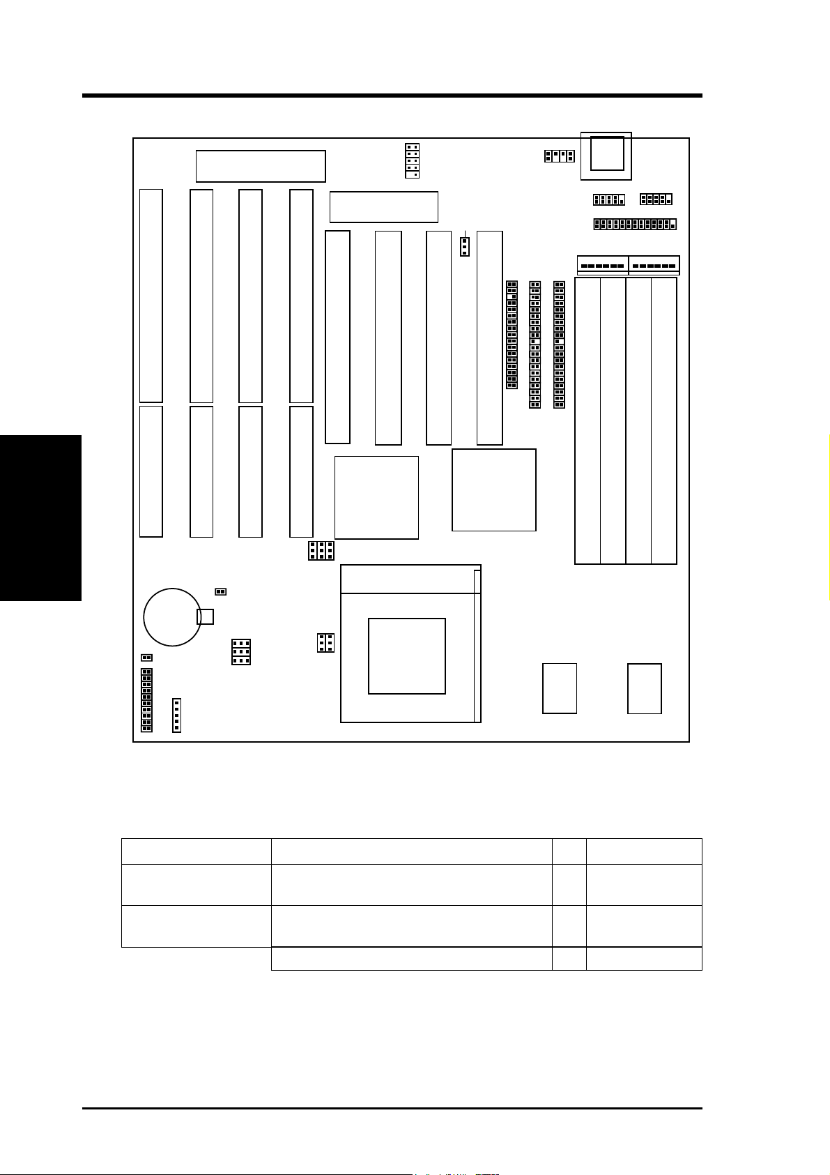
8 VX97 User’s Manual
III. INSTALLATION
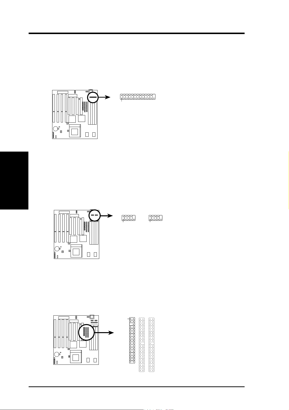
(Jumpers)
III. INSTALLATION
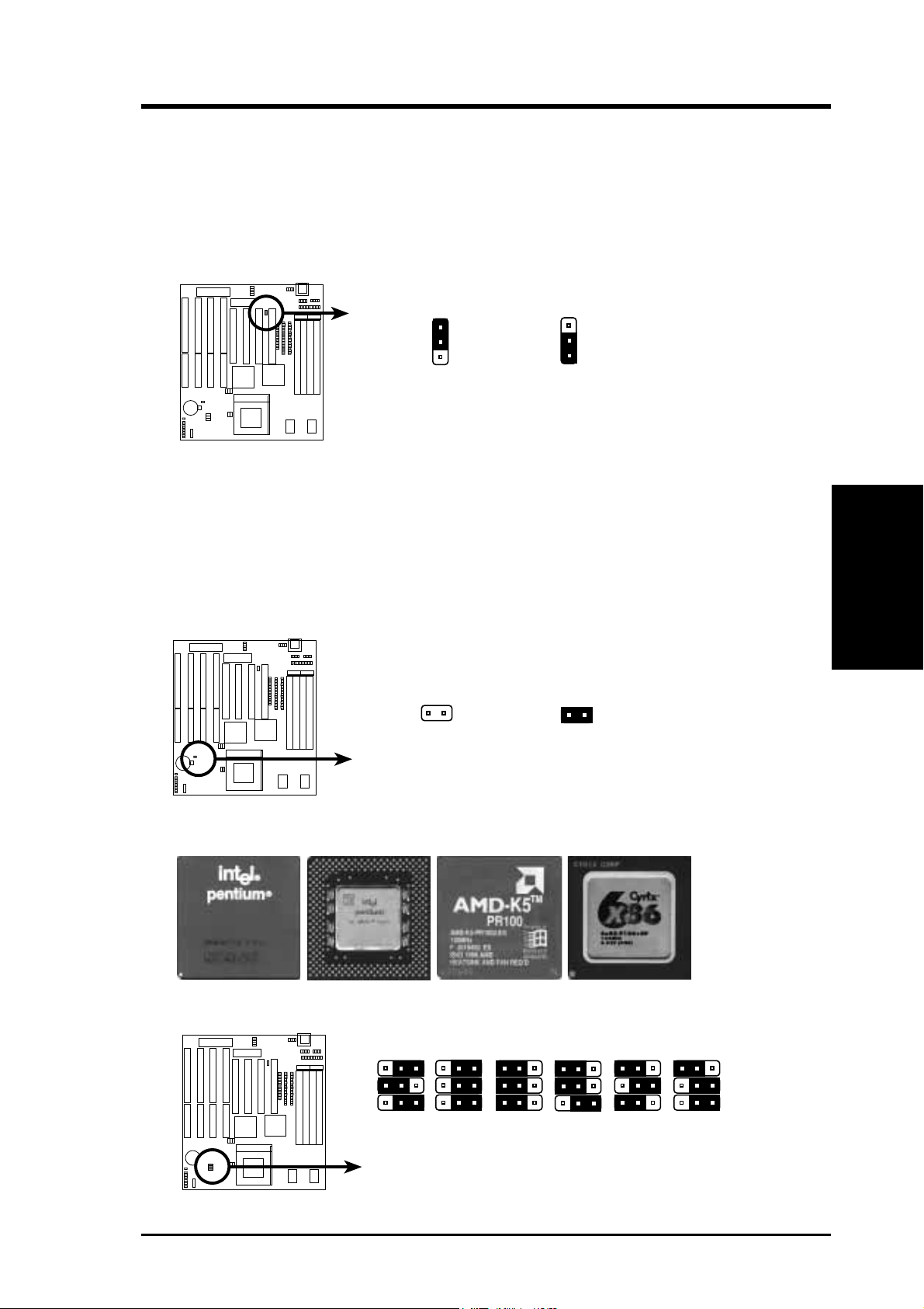
4. CPU External (BUS) Frequency Selection (FS0, FS1, FS2)
These jumpers tell the clock generator what frequency to send to the CPU. These
allow the selection of the CPU’s External frequency (orBUS Clock). The BUS Clock
timesthe BUSRatio equalsthe CPU'sInternal frequency(the advertisedCPU speed).
5. CPU to BUS Frequency Ratio (BF0, BF1)
These jumpers set the frequency ratio between the Internal frequency of the CPU
and the External frequency (called the BUS Clock) within the CPU. These must
be set together with the above jumpers CPU External (BUS) Frequency Selection.
50MHz 55MHz 60MHz 66MHz
CPU External Clock (BUS) Frequency Selection
FS1
1
2
3
FS0
FS2
FS1
1
2
3
FS0
FS2
FS1
1
2
3
FS0
FS2
FS1
1
2
3
FS0
FS2
CPU : BUS Frequency Ratio
1.5x (3/2)
BF1
BF0
2.0x(2/1)
BF1
BF0
2.5x (5/2)
BF1
BF0
3.0x (3/1)
BF1
BF0
3.0x (3/1) 2.0x(2/1) 1.0x (1/1) 4.0x (4/1)
Intel
Cyrix
Set the jumpers by the Internal speed of the Intel, AMD, or Cyrix CPU as follows:
(BUS Freq.) (Freq. Ratio)
CPU Model Freq. Ratio BUS Freq. FS2 FS1 FS0 BF1 BF0
Intel Pentium 200MHz 3.0x 66MHz [2-3] [1-2] [2-3] [2-3] [1-2]
Intel Pentium 166MHz 2.5x 66MHz [2-3] [1-2] [2-3] [2-3] [2-3]
Intel Pentium 150MHz 2.5x 60MHz [2-3] [2-3] [1-2] [2-3] [2-3]
Intel Pentium 133MHz 2.0x 66MHz [2-3] [1-2] [2-3] [1-2] [2-3]
Intel Pentium 120MHz 2.0x 60MHz [2-3] [2-3] [1-2] [1-2] [2-3]
Intel Pentium 100MHz 1.5x 66MHz [2-3] [1-2] [2-3] [1-2] [1-2]
Intel Pentium 90MHz 1.5x 60MHz [2-3] [2-3] [1-2] [1-2] [1-2]
Intel Pentium 75MHz 1.5x 50MHz [2-3] [2-3] [2-3] [1-2] [1-2]
AMD-K5-PR133 100MHz 1.5x 66MHz [2-3] [1-2] [2-3] [1-2] [1-2]
AMD-K5-PR120 90MHz 1.5x 60MHz [2-3] [2-3] [1-2] [1-2] [1-2]
AMD-K5-PR100 100MHz 1.5x 66MHz [2-3] [1-2] [2-3] [1-2] [1-2]
AMD-K5-PR90 90MHz 1.5x 60MHz [2-3] [2-3] [1-2] [1-2] [1-2]
AMD-K5-PR75 75MHz 1.5x 50MHz [2-3] [2-3] [2-3] [1-2] [1-2]
*Cyrix 166+ 133MHz 2.0x 66MHz [2-3] [1-2] [2-3] [1-2] [2-3]
*NOTE: Only Cyrix Revision 2.7 or later is supported on this motherboard. See previous page for
revision identification. Bootup screen will show 6x86-P166+ -S CPU at 133MHz with the
Cyrix 166+ installed on this motherboard.
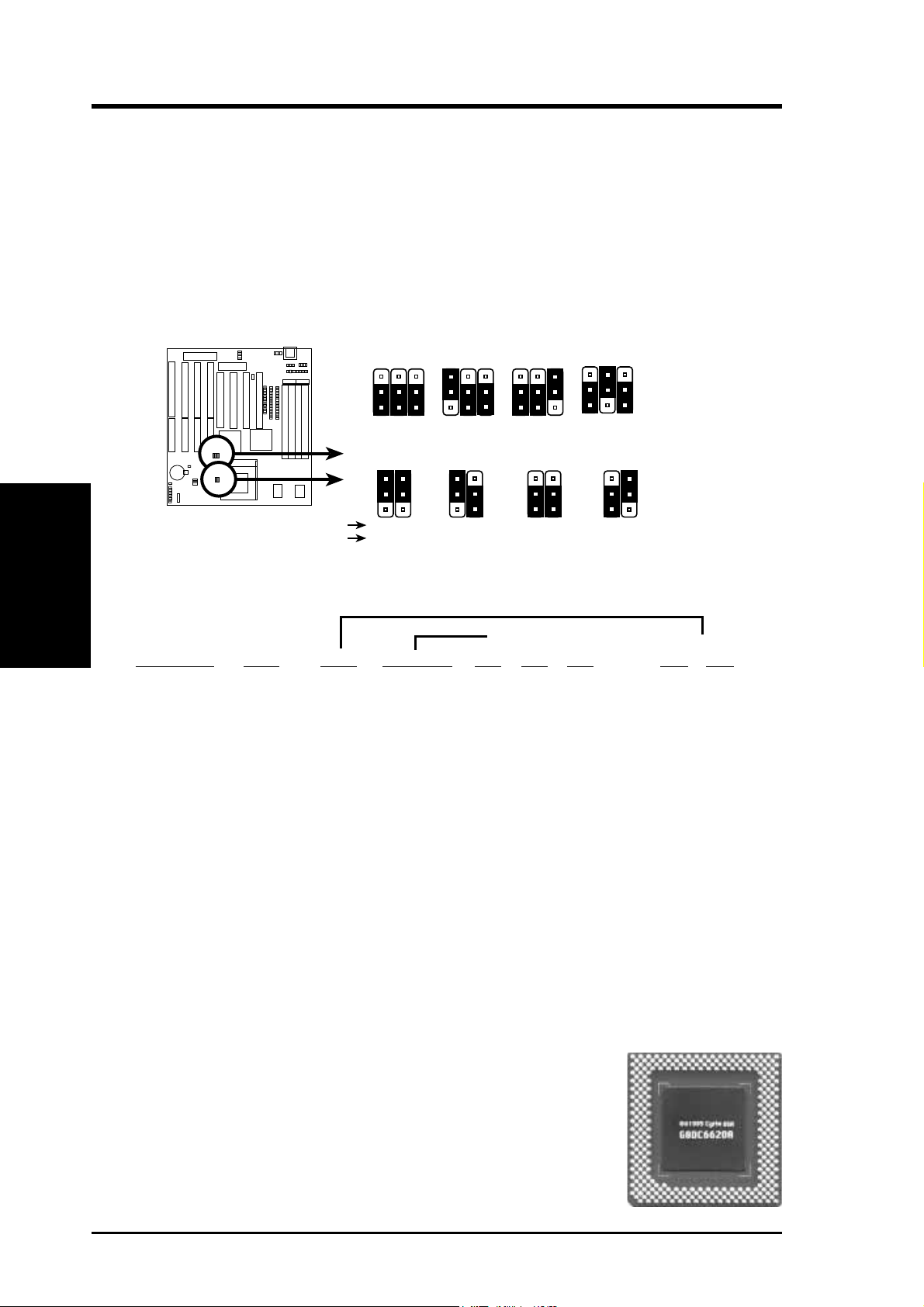
Compatible Cyrix CPU Identification
The only Cyrix CPU that is supported on this motherboard is
labeled Cyrix 6x86 P166+ but must be Revision 2.7 and later.
Look on the underside of the CPU for the serial number. The
number should read G8DC6620Aor larger.