7
ATA6612/ATA6613/ATA6614 [APPLICATION NOTE]
9127E–AUTO–03/15
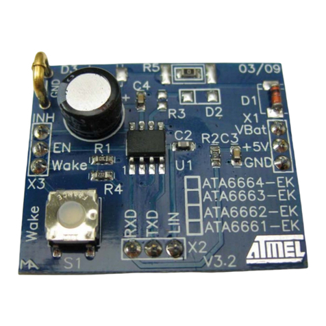
The microcontroller pin PD3 is used by default to trigger the watchdog. In order to lead the signals generated from pin PD3
to the watchdog trigger input NTRIG, the jumper TRIG has to be set. If it is not possible to use the pin PD3 to trigger the
watchdog as it is being used for another function, remove the TRIG jumper completely and connect the NTRIG pin directly to
another microcontroller pin using a 1-wire cable.
If the watchdog is not used, the trigger input can be left open on the development board, as it is equipped with an internal
pull-up resistor. For normal use of the Atmel®ATA6612, the Atmel ATA6613 and the Atmel ATA6614 with deactivated
watchdog, it is recommended that the trigger input pin NTRIG is tied directly to VCC for EMC reasons.
Replacing the resistor R8 results in a frequency change of the internal oscillator. This in turn results in different watchdog
timing. The following formula demonstrates how the frequency of the internal oscillator depends on the value of the resistor
R8. Refer also to the Atmel ATA6612/ATA6613/ATA6614 datasheet for further information:
tOSC [RWD_OSC] = 0.405 RWD_OSC – 0.0004 x (RWD_OSC)2
tOSC in µs, RWD_OSC in k
With the values given in the datasheet, you can calculate all relevant watchdog times (for example the open window and the
closed window) using tOSC.
In general, the Atmel ATA6612, ATA6613 and ATA6614 are shipped with an oscillator start-up time of 65ms. Due to the
extra-long lead time of 155ms it should be possible in almost all cases to meet the first open window of the watchdog. If more
time is needed, the default start-up time of the microcontroller 65ms can be reduced via the fuse bits to 4.1ms or even 0ms.
The IC mounted on the board is delivered with a start-up time of 65ms.
3.1.4 LIN Interface (LIN, TXD and RXD)
The LIN Transceiver is only active when the LIN SBC is in the normal mode. In all other modes the transceiver is switched
off and no signals from the microcontroller will be transmitted to the bus and no signals from the bus will be given to the
microcontroller.
As the two pins TXD and RXD on the LIN SBC are controlled by the microcontroller's UART, they are connected to the
corresponding TXD and RXD pins on the microcontroller via a zero ohm resistor. For monitoring the signals at these pins,
test points are provided on the development board.
3.1.4.1 LIN Pin
A low-side driver with internal current limitation and thermal shutdown and an internal pull-up resistor in compliance with LIN
spec 2.x are implemented. LIN receiver thresholds are compatible with the LIN protocol specification.
When using the development board for a LIN master application, it is possible to mount the two necessary extra components
diode D2 (e.g., LL4148) in series with resistor R1 (1k) on the board at their designated placeholders.
3.1.4.2 TXD Input/Output Pin (LIN SBC)
The signals given to the TXD input pin control the state of the LIN output. The TXD input pin must be pulled to Ground in
order to have the LIN bus low. If TXD is high, the LIN output transistor is turned off and the bus is in recessive state, pulled
up by the internal/external resistor. If TXD is low, the LIN output transistor is turned on and the bus is in dominant state. An
internal timer prevents the bus line from being driven permanently in the dominant state. If TXD is forced to low longer than
tDOM, the LIN SBC switches the TXD state internally to high and the LIN bus driver is switched to the recessive state.
This feature is used to avoid that either a single faulty slave node or a short to Ground at the TXD pin can paralyze the
communication on the complete LIN bus to which the faulty slave node is connected. Due to this behavior, the internal state
of the TXD pin can differ from the signal level visible at the pin itself. However, if TXD is short-circuited to GND, it is possible
to switch to sleep mode via pin EN after tDOM_max.
3.1.4.3 TXD Input/Output Pin (Microcontroller)
The TXD-pin from the microcontroller, belonging to the hardware UART, is hard-wired to the TXD input pin from the LIN SBC
via a 0resistor.
As the LIN SBC indicates the wake-up source (local wake-up or remote wake-up) with the help of the TXD pin it is
recommended that the TXD pin from the microcontroller will be reconfigured as an input when entering silent mode or sleep
mode. Please note that the Atmel ATA6624 inside the Atmel ATA6612 and the Atmel ATA6613 signals the wake-up
source in a different way as the Atmel ATA6630 inside the Atmel ATA6614. Additionally at the Atmel ATA6614 a VS
undervoltage is also signaled. As long as pin EN is still low after a wake-up the LIN SBC signals the wake-up source on
pin TXD.
