Ublox EVK-NORA-W10 User manual

UBX-22002764 - R01
C1-Public www.u-blox.com
EVK-NORA-W10
Evaluation kit for NORA-W10 series modules
User guide
Abstract
The document describes how to set up the EVK-NORA-W101 and EVK-NORA-W106 evaluation kits
to evaluate the NORA-W10 series modules. To obtain the different options for debugging and the
development capabilities included in the evaluation board see NORA-W10 system integration
manual [2].

EVK-NORA-W1 - User guide
UBX-22002764 - R01 Document information Page 2 of 22
C1-Public
Document information
Title
EVK-NORA-W1
Subtitle
Evaluation kit for NORA-W10 series modules
Document type
User guide
Document number
UBX-22002764
Revision and date
R01
3-May-2022
Disclosure restriction
C1-Public
Product status
Corresponding content status
In development /
Prototype
Objective specification
Target values. Revised and supplementary data will be published later.
Engineering sample
Advance information
Data based on early testing. Revised and supplementary data will be published later.
Initial production
Early production information
Data from product verification. Revised and supplementary data may be published later.
Mass production/
End of life
Production information
Document contains the final product specification.
This document applies to the following products:
Product name
Document status
EVK-NORA-W101
Objective specification
EVK-NORA-W106
Objective specification
☞For information about the hardware, software, and status of the available product types, see the
NORA-W10 data sheet [1].
u-blox or third parties may hold intellectual property rights in the products, names, logos and designs included in this
document. Copying, reproduction, modification or disclosure to third parties of this document or any part thereof is only
permitted with the express written permission of u-blox.
The information contained herein is provided “as is” and u-blox assumes no liability for its use. No warranty, either express or
implied, is given, including but not limited to, with respect to the accuracy, correctness, reliability and fitness for a particular
purpose of the information. This document may be revised by u-blox at any time without notice. For the most recent
documents, visit www.u-blox.com.
Copyright © u-blox AG.

EVK-NORA-W1 - User guide
UBX-22002764 - R01 Contents Page 3 of 22
C1-Public
Contents
Document information................................................................................................................................2
Contents ..........................................................................................................................................................3
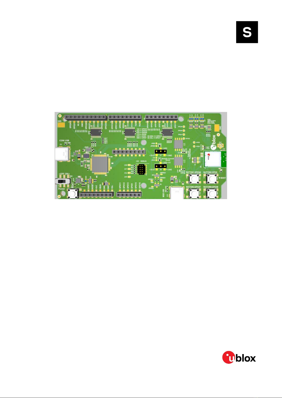
1Product description ..............................................................................................................................4
1.1 Key features .................................................................................................................................................4
1.2 Items included in kit.................................................................................................................................... 5
1.2.1 EVK-NORA-W101 kit contents........................................................................................................5
1.2.2 EVK-NORA-W106 kit contents........................................................................................................5
2Setting up the evaluation board.......................................................................................................6
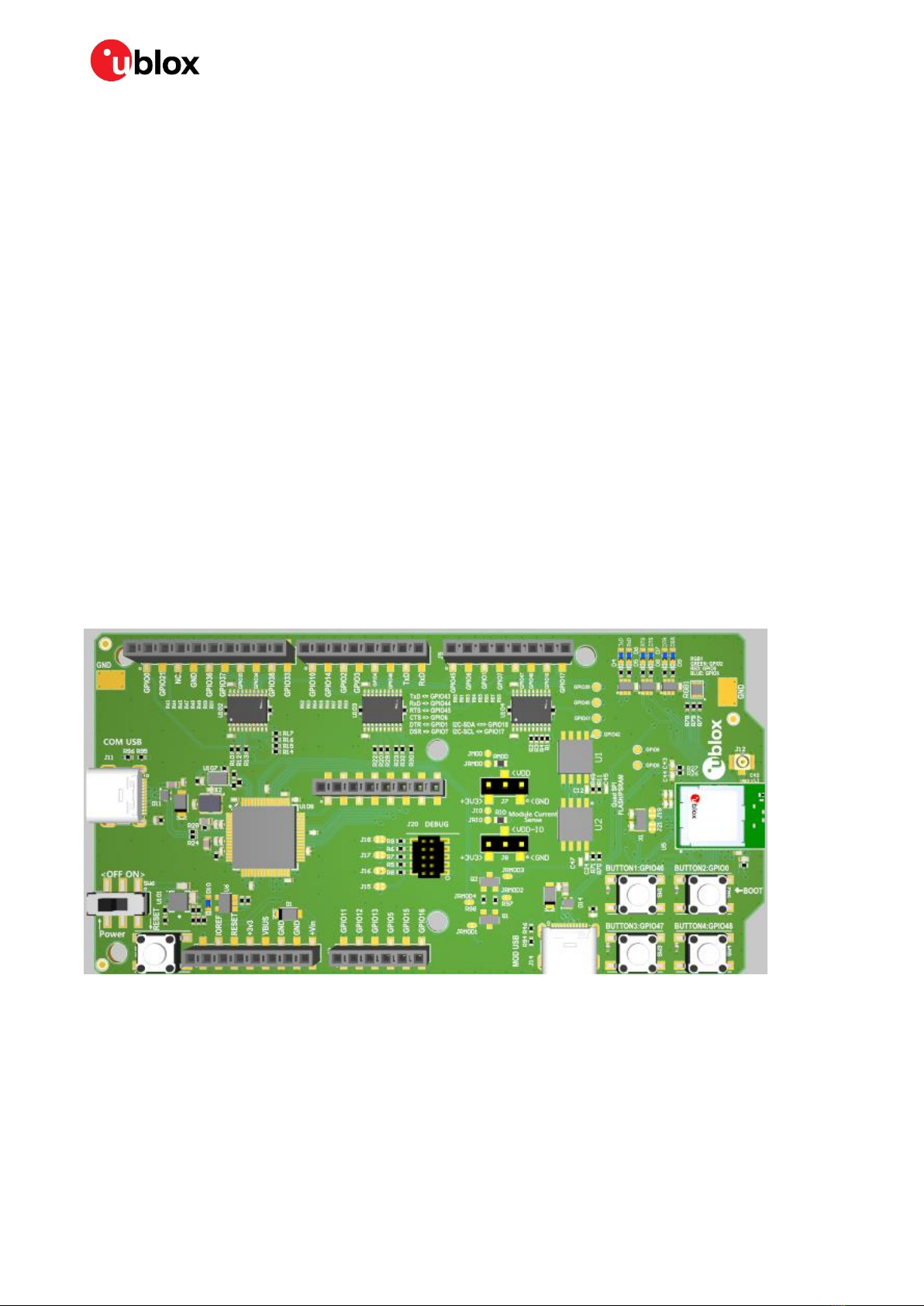
3Hardware description...........................................................................................................................7
3.1 Power .............................................................................................................................................................7
3.1.1 Powering the board ............................................................................................................................7
3.2 Reset..............................................................................................................................................................8
3.3 Buttons..........................................................................................................................................................9
3.4 LEDs.............................................................................................................................................................10
3.5 Serial communication ..............................................................................................................................11
3.6 32.768 kHz low frequency clock.............................................................................................................12
3.7 Current sensing headers .........................................................................................................................13
3.8 External JTAG debug interface..............................................................................................................14
3.9 QSPI .............................................................................................................................................................15
3.10 GPIO jumpers .............................................................................................................................................16
3.11 Header pin-out ...........................................................................................................................................17
Appendix ....................................................................................................................................................... 20
AGlossary ................................................................................................................................................. 20
Related documentation ........................................................................................................................... 21
Revision history.......................................................................................................................................... 21
Contact.......................................................................................................................................................... 22

EVK-NORA-W1 - User guide
UBX-22002764 - R01 Product description Page 4 of 22
C1-Public
1Product description
The EVK-NORA-W10 evaluation kit provides stand-alone use of the NORA-W10 series module.
All features of the NORA-W10 series modules are easily accessed from the evaluation board. A simple
USB connection provides power, programming, and COM ports. Four user buttons are available, as
well as a USB peripheral connector, user LEDs, and a reset button.
GPIO signals are available on headers that are compatible with the Arduino® form factor. This allows
easy use of existing Arduino shields. Current sense resistors allow for measuring current into the
module and into the shield.
This guide provides setup instructions for starting development and describes the hardware
functionality of the EVK-NORA-W10 board.
1.1 Key features
•Used for evaluation of NORA-W101 or NORA-W106 modules
•COM ports and debug ports over USB
•Full GPIO of the NORA-W1 series
•Buttons and LEDs for user interaction
•32.768 kHz Crystal
•USB peripheral connector
•Power input via USB-C or pin sockets
•Current measurements via pin headers and jumpers
Figure 1: EVK-NORA-W10 evaluation board (top view)

EVK-NORA-W1 - User guide
UBX-22002764 - R01 Product description Page 5 of 22
C1-Public
1.2 Items included in kit
1.2.1 EVK-NORA-W101 kit contents
•EVK-NORA-W10 evaluation board with NORA-W101 module
•USB-C to USB-A cable
•2.4 GHz U.FL antenna kit
1.2.2 EVK-NORA-W106 kit contents
•EVK-NORA-W10 evaluation board with NORA-W106 module
•USB-C to USB-A cable
•2.4 GHz antenna integrated onto NORA-W106 module (no external antenna)

EVK-NORA-W1 - User guide
UBX-22002764 - R01 Setting up the evaluation board Page 6 of 22
C1-Public
2Setting up the evaluation board
The EVK-NORA-W10 is delivered without any software (open CPU) and the software must be
developed by the user.
The following devices are applicable:
•EVK-NORA-W101
•EVK-NORA-W106
The module is designed to be used only with the applicable software and only compatible software
can be flashed on the module.
Connect external power supply to the EVK as described in Powering the board. The status light (D10)
(green) lights up, indicating that the internal EVK 3.3 V is on.
⚠When using the evaluation board with external antenna, before powering up the EVK, ensure that
you have connected the 2.4 GHz antenna with the U.FL antenna connector (J12). Failing to do so
may cause undesired operation.
⚠Observe that the inrush current when powering-up the EVK can be significantly higher than during
normal operation.
The operating system will install the correct COM port drivers automatically. The drivers will need to
be installed only when you connect the unit to a new computer for the first time. For more information
about the COM ports and their configuration, see the FTDI FT231XQ-R Datasheet [3].
One COM port will automatically be assigned to the unit by the Windows OS. To view the assigned
COM ports on Windows 10, follow the steps mentioned below:
•Open the Control Panel and click Hardware and Sound.
•Click Device Manager in Devices and Printers. This will open the Device Manager window where
you can view the assigned COM ports.
The NORA-W10 open CPU variants are to be used when developing custom software based on the
Espressif SDK ESP-IDF. Before compiling custom software, the ESP-IDF must be configured for the
NORA-W10 open CPU variant.
More information on this topic can be found in the NORA-W10 system integration manual [2].

EVK-NORA-W1 - User guide
UBX-22002764 - R01 Hardware description Page 7 of 22
C1-Public
3Hardware description
Design files for the EVK-NORA-W10 PCB may be requested from your local u-blox support team.
3.1 Power
The EVK-NORA-W1 has three possible power sources, as listed below:
•USB from the debug interface
•USB peripheral on the NORA-W1 itself
•2.54 mm pitch pin header (J1 pin-8) for supplying + 5 V [ 3.6 –5.5 V]
Each of the three power sources are separated via a Schottky diode (D1 –D3, MBR120VLSFT3G). This
prevents reverse voltage to any of the other supplies thus the power sources can be connected
simultaneously.
⚠Only if the power protection circuits are left intact can the USB be safely connected at the same
time as external power. This makes programming of the module easier.
⚠The EVK USB type C connectors are only capable of handling 5 V input, 12 V is not allowed.
3.1.1 Powering the board
By moving the power switch to “ON” VBUS is fed into the 3.3 V LDO regulator and the board is
powered-up. This is indicated by the power LED D10 (green) lights up. The LDO regulator powers the
+3V3, VDD, and VDD-IO power rails.
Figure 2: EVK schematic - power supply
Figure 3: EVK schematic - IOREF separation
+3V3 (J1 pin 4) can source max 50 mA to supply external parts.
IOREF (J1 pin 2) is the external supply input to the IO voltage level shifters (optional). It is separated
from +3V3 with a protection diode (Maxim MAX40203AUK) having voltage drop of 28 mV at 100 mA.

EVK-NORA-W1 - User guide
UBX-22002764 - R01 Hardware description Page 8 of 22
C1-Public
3.2 Reset
The EVK-NORA-W10 provides a hardware reset to the NORA-W10 module. The Reset button is
connected to the module RESETn signal.
If the BOOTn button is held down during the EVK power on, it causes the module to enter its
bootloader mode.
Figure 4: EVK schematic - reset and boot buttons
Figure 5: Alternative BOOTn and RESET via UART-DTR and RTS
Signal name
Description
GPIO0/BOOTn
GPIO0 input to module interface during normal operation.
Drive low during power-up to enter bootloader mode on NORA-W1 module.
RESETn
NORA-W1 reset signal.
Table 1: EVK reset signals

EVK-NORA-W1 - User guide
UBX-22002764 - R01 Hardware description Page 9 of 22
C1-Public
3.3 Buttons
The evaluation board has four user buttons that are active low and connect to ground when pressed.
Table 2 associates the button number and corresponding components.
The internal pull-up resistor of each NORA-W10 GPIO pin must be enabled for proper operation.
Button
Switch
GPIO
Protection diode
1
SW1
GPIO46
D21
2
SW2
GPIO0
D22
3
SW3
GPIO47
D23
4
SW4
GPIO48
D24
Table 2: User button components
Figure 6: EVK schematic - user buttons

EVK-NORA-W1 - User guide
UBX-22002764 - R01 Hardware description Page 10 of 22
C1-Public
3.4 LEDs
A RGB LED is provided on the evaluation board. It is powered by +3V3 and turned on by pulling the
associated GPIO low.
The RGB LED can be disconnected from the GPIO by removing the associated resistor R78 –R79.
The evaluation board is also equipped with LEDs that shows the signal status of UART0
RGB LED
Associated GPIO
Comments
Red (pin1)
GPIO5/ADC1-CH4
Remove R77 to disconnect R-LED
Green (pin2)
GPIO2/ADC-CH1
Remove R78 to disconnect G-LED
Blue (pin3)
GPIO8/ADC1-CH7
Remove R79 to disconnect B-LED
Table 3: RGB LED associated signals
Figure 7 Schematic –RGB and power LED
Figure 8 Schematic –UART0 status LEDs
Table 4: UART0 LEDs associated signals
LED
LED color
GPIO
Pin socket
Comments
D4
Green
GPIO43/UART0-TxD
J3-7
D5
Orange
GPIO44/UART0-RxD
J3-8
D6
Green
GPIO45/UART0-RTS
J5-1
D7
Orange
GPIO6/UART0-CTS
J5-2
D8
Green
GPIO1/UART0-DTR
J5-3
D9
Orange
GPIO7/UART0-DSR
J5-4
D10
Green
-
Power ON LED
RGB-LED
UART0 status LED

EVK-NORA-W1 - User guide
UBX-22002764 - R01 Hardware description Page 11 of 22
C1-Public
3.5 Serial communication
The evaluation board allows for easy serial communication with the NORA-W10 module and a
connected computer. The EVK is using a single FTDI interface IC providing one COM port.
•The single port is connected to module UART0 through 1K resistors. This allows for simultaneously
connecting UART0 signals to pin sockets J3 and J5. See also Table 5.
NORA-W1 pin name
NORA-W1 function
Resistor/Jumper enable
Interface IC function
G9
GPIO44/UART0-RxD
R20
FTDI-TxD
G8
GPIO43/UART0-TxD
R22
FTDI-RxD
F9
GPIO6/UART0-CTS
R23
FTDI-RTS
F8
GPIO45/UART0-RTS
R29
FTDI-CTS
E9
GPIO7/UART0-DSR
R30
FTDI-DTR
E8
GPIO1/UART0-DTR
R32
FTDI-DSR
Table 5: COM port connections
Figure 9: UART0 level shifters and pin socket

EVK-NORA-W1 - User guide
UBX-22002764 - R01 Hardware description Page 12 of 22
C1-Public
Figure 10: The FTDI drawing, 1 port default
3.6 32.768 kHz low frequency clock
The evaluation board has a 32.768 kHz crystal connected to the NORA-W10 module to allow use of
the external crystal oscillator option
If the signals GPIO15/ADC2-CH4 and GPIO16/ADC2-CH5 want to be used, the crystal can be removed
from the circuit by opening jumpers J19 and J21 and soldering across the normally open positions.
This connects XT-32k-p and XT-32k-n to the EVK pin socket J2 pin 5 and pin 6.
Figure 11: Schematic –32 kHz crystal

EVK-NORA-W1 - User guide
UBX-22002764 - R01 Hardware description Page 13 of 22
C1-Public
3.7 Current sensing headers
The evaluation board provides two current sensing headers:
•J7 allows for power consumption measurement of the NORA-W10 module VDD supply.
•J8 allows for power consumption measurement of the NORA-W10 module VDD-IO supply.
Each of the 2.54 mm pitch 3-pin header have two pins connected across a 1 Ωcurrent-sense resistor
and the third pin connected to GND. Module VDD supply and module VDD-IO supply is sourced via
these resistors. To measure current consumption, use a multimeter or other precision voltage
measurement device to measure voltage drop across pins 2 and 3. Current can also be measured
directly by opening JRMOD, or JRIO to remove the current-sense resistor from the circuit. Use an amp
meter in series with the two voltage pins.
⚠Pin 1 of J7, J8 is connected to GND.
Any current sense resistor can be bypassed by soldering the respective jumper: JMOD, or JIO.
The default hardware configuration does not require any modification of the current sense headers
for the EVK-NORA-W10 to perform properly.
Figure 12: Current sensing header layout

EVK-NORA-W1 - User guide
UBX-22002764 - R01 Hardware description Page 14 of 22
C1-Public
3.8 External JTAG debug interface
External target hardware can be connected to J20 for firmware programming and debug. The JTAG
debug interface is implemented, as shown in Figure 13.
J20 is implemented with a 2x5, header with 1.27 mm pitch.
Figure 13: External J-Link debug interface

EVK-NORA-W1 - User guide
UBX-22002764 - R01 Hardware description Page 15 of 22
C1-Public
3.9 QSPI
EVK-NORA-W10 can be populated with a Quad SPI FLASH and a Quad SPI PSRAM. These can be
supplied via +3V3 or NORA-W10 module internal VDD-SPI supply. The selection between the two are
made by populating either R11 or R69 (U1) and R70 or R71 (U2).
Figure 14: Quad SPI FLASH and PSRAM EVK - schematic and EVK board view
Table 6: Quad SPI interface signal overview
Interface function
ESP32-S3 pin
NORA-W10 pin
Interface IC function
QSPI-CS0
28
E1
QSPI-CS1
32
C4
QSPI-CLK
33
F1
QSPI-IO3 HD
30
F2
QSPI-IO2 WP
31
D1
QSPI-IO1 Q
34
E2
QSPI-IO0 D
35
D2

EVK-NORA-W1 - User guide
UBX-22002764 - R01 Hardware description Page 16 of 22
C1-Public
3.10 GPIO jumpers
Several solder bridge jumpers on the board are available to configure the GPIO functions. Most solder
jumpers disconnect on-board components from the GPIO nets thus eliminate interference with
external circuitry added on the I/O sockets (female).
The GPIO jumpers and associated functions are shown on the bottom of the EVK-NORA-W10 PCB.
Figure 15: Legend for GPIO jumpers

EVK-NORA-W1 - User guide
UBX-22002764 - R01 Hardware description Page 17 of 22
C1-Public
3.11 Header pin-out
Figure 14 shows the 2.54 mm pitch sockets exposing the IO signals in the NORA-W10 module.
Figure 16: EVK-NORA-W10 IO connectors pin-out, buttons and LEDs
⚠To enable the EVK-NORA-W10 I/O pins to handle 5 V signals the level shifters (U102 –U104, TI
TXS0108EPWR) must be populated and IOREF must be supplied with +5 V. If using 3.3 V on the
EVK-NORA-W1 I/O pins, the Arduino Uno® style shields must be configured to use +3.3 V I/O
voltage reference.
GPIO8
GPIO9
NC.
IOREF
RESET
+3V3
VBUS
GND
GND
+Vin
GPIO11
GPIO12
GPIO13
GPIO5
GPIO15
GPIO16
GPIO0
GPIO21
NC.
GND
GPIO36
GPIO37
GPIO35
GPIO34
GPIO38
GPIO33
GPIO10
GPIO14
GPIO2
GPIO3
GPIO4
GPIO46
TxD
RxD
GPIO45
GPIO6
GPIO1
GPIO7
GPI047
GPIO48
GPIO18
GPIO17
LED4:TxD
LED6:RTS
LED5:RxD
LED7:CTS
LED8:DTR
LED9:DSR
BTN1:GPIO46
BTN2:GPIO0
BTN3:GPIO47
BTN4:GPIO48
RGB LED
RF-port
POWER LED D10
POWER SW6
RESET BTN
J1
J2
J3
J4
J9
J5
Buttons and switches
Not connected
IO-signals
Color code
LEDs
Supply voltage
Ground connection
Pin-1 indicator
GPIO42
GPIO41
GPIO40
GPIO39

EVK-NORA-W1 - User guide
UBX-22002764 - R01 Hardware description Page 18 of 22
C1-Public
Table 7: Header J1Table 7 - Table 12 show the pin assignments of each header.
Pin
Pin name
NORA-W1 pin
Function
1
NC.
-
No connection
2
IOREF
-
Level shifter supply voltage
3
RESET
J3
ESP-GPIO/AIN6
4
+3V3
–
Supply
5
VBUS
Supply
6
GND
Ground
7
GND
Ground
8
+Vin
Supply
Table 7: Header J1
Pin
Pin name
NORA-W1 pin PT1/PT2
Function
1
GPIO11
G3
GPIO ADC2-CH0
2
GPIO12
G2
GPIO ADC2-CH1
3
GPIO13
A6
GPIO ADC2-CH2
4
GPIO5
J8
GPIO ADC1-CH4
5
GPIO15
C6
GPIO ADC2-CH4, XTAL-32K-P
6
GPIO16
B6
GPIO ADC2-CH5, XTAL-32K-N
Table 8: Header J2
Pin
Pin name
NORA-W1 pin
Function
1
GPIO10
H3
FSPI-IO4
2
GPIO14
A5
FSPI-DQS
3
GPIO2
H8
ADC1-CH1
4
GPIO3
J9
ADC-CH2
5
GPIO4
D8
ADC1-CH3
6
GPIO46
H7
GPIO46
7
TxD
G8
GPIO43
8
RxD
G9
GPIO44
Table 9: Header J3

EVK-NORA-W1 - User guide
UBX-22002764 - R01 Hardware description Page 19 of 22
C1-Public
Pin
Pin name
NORA-W1 pin
Function
1
GPIO0
F7
BOOTn
2
GPIO21
C8
GPIO21
3
NC.
–
4
GND
–
5
GPIO36
B1
FSPI-CLK
6
GPIO37
C1
FSPI-Q
7
GPIO35
C2
FSPI-D
8
GPIO34
B3
FSPI-CS0
9
GPIO38
A2
FSPI-WP
10
GPIO33
D3
FSPIHD
Table 10: Header J4
Pin
Pin name
NORA-W1 pin
Function
1
GPIO45
F8
RTS
2
GPIO6
F9
CTS
3
GPIO1
E8
DTR
4
GPIO7
E9
DSR
5
GPIO47
F3
SPICLK_P
6
GPIO48
E3
SPICLK_N
7
GPIO18
B4
SDA
8
GPIO17
A3
SCL
Table 11: Header J5
Pin
Pin name
NORA-W1 pin
Function
1
+3V3
-
Supply
2
JTAG-TMS
H2
GPIO42 if J15 is changed
3
GND
-
Ground
4
JTAG-TCK
J2
GPIO-39 if J16 is changed
5
GND
-
Ground
6
JTAG-TDO
G1
GPIO40 if J17 is changed
7
NC.
-
No connection
8
JTAG-TDI
H1
GPIO41 if J18 is changed
9
GND
-
Ground
10
RESET
J3
Module reset
Table 12: Header J20

EVK-NORA-W1 - User guide
UBX-22002764 - R01 Appendix Page 20 of 22
C1-Public
Appendix
AGlossary
Abbreviation
Definition
ARM
Arm (Advanced RISC Machines) Holdings
CPU
Central Processing Unit
CTS
Clear To Send
DC
Direct Current
DC-DC
DC to DC converter
DFU
Device Firmware Update
EVK
Evaluation Kit
FICR
Factory Information Configuration Register
GPIO
General Purpose Input / Output
LDO
Low Drop-Out voltage regulator
LE
Low Energy
LED
Light Emitting Diode
LF
Low Frequency
LiPo
Lithium-Polymer battery
NCS
nRF Connect SDK
NFC
Near-Field Communications
QSPI
Quad Serial Peripheral Interface
RC
Resistor-Capacitor network
RTS
Request To Send
RXD
Receive data signal
SES
SEGGER Embedded Studio
SIG
Special Interest Group
SoC
System on Chip
SPI
Serial Peripheral Interface
TXD
Transmit data signal
UICR
User Information Configuration Register
USB
Universal Serial Bus
Table 13: Explanation of the abbreviations and terms used
Table of contents
Other Ublox Motherboard manuals

Ublox
Ublox EVK-N2 Series User manual

Ublox
Ublox EVK-U20 User manual

Ublox
Ublox EVK-8 User manual

Ublox
Ublox EVK-JODY-W2 User manual

Ublox
Ublox C102-F9R User manual

Ublox
Ublox EVK-M8U User manual

Ublox
Ublox C93-M8E User manual

Ublox
Ublox EVK-M8F-0-01 User manual

Ublox
Ublox EVK-M8 User manual

Ublox
Ublox EVK-NINA-B3 Series User manual

Ublox
Ublox EVK-F9DR User manual

Ublox
Ublox BMD-3 Series User manual

Ublox
Ublox C94-M8P User manual

Ublox
Ublox EVK-M101 User manual

Ublox
Ublox EVK-G31 User manual

Ublox
Ublox EVK-M8T User manual

Ublox
Ublox EVK-L4 User manual

Ublox
Ublox XPLR-AOA-3 User manual

Ublox
Ublox C099-F9P User manual

Ublox
Ublox XPLR-AOA User manual