Asahi KASEI AKD4709-A User manual

ASAHI KASEI [AKD4709-A]
<KM103002> 2011/06
GENERAL DESCRIPTION
AKD4709 is an evaluation board for quickly evaluating the AK4709, AV SCART switch. Evaluation
requires audio/video analog analyzers/generators and a power supply.
Ordering guide
AKD4709-A --- AK4709 Evaluation Board
(Cable for connecting with printer port of IBM-AT,
compatible PC and control software are packed with this.)
FUNCTION
•RCA connectors for analog audio input/output
•XLR connectors for analog audio input
•RCA connectors for analog video input/output
•10pin header for serial control interface
AK4709
AINL+
AINL
AINR
(AINR+-)
VD1 VD2 AGND
TVINL
TVINR
VCRINL
VCRINR
TVOUTL
TVOUTR
VCROUTL
VCROUTR
VCRFB
TVFB
TVSB
VCRSB
ENCB
ENCC
ENCG
ENCV
ENCY
ENCRC
TVVOUT
TVB
TVG
TVRC
VCRVOUT
TVVIN
VCRVIN
VCRB
VCRG
VCRRC
VCRC
VVD2
Buffer
10pin header
VVD1
Regulator
VVD
VP
+12V →+3.3V
VSS2
(AINL+-)
AINR+
Figure 1. AKD4709 Block Diagram
* Circuit diagram and PCB layout are attached at the end of this manual.
AK4709 Evaluation Board Rev.2
AK
D470
9
-
A
- 1 -

ASAHI KASEI [AKD4709-A]
<KM103002> 2011/06
EVALUATION BOARD MANUAL
Operation sequence
1) Set up the power supply lines.
Name of
Jack
Color of
Jack Voltage Used for Comment and attention Default of
Jack
VP Orange
+10.8∼+13.2V VP of AK4709 Should be always connected +12V
VD1 Red
+3.13∼+3.47 VD1 of AK4709
Should be connected when jp5 (VD1_SEL) is
set to REG side.
Should be open when JP5 (VD1_SEL) is set to
VD1 side.
open
VD2 Red
+3.13∼+3.47V VD2 of AK4709
Should be connected when R 56(VD2_SEL) is
set to REG side.
Should be open when R56 (VD2_SEL) is set to
VD2 side.
open
VVD Red
+3.13∼+3.47V VVD1 of AK4709
VVD2 of AK4709
Should be connected when JP8 (VVD_SEL) is
set to REG side.
Should be open when JP8 (VVD_SEL) is set to
VVD side.
open
VCC Red +3.13 ∼
VVD1+0.3V
Power supply of
logic
Should be connected when JP7 (VCC_SEL) is
set to REG side.
Should be open when JP7 (VCC_SEL) is set to
VCC side.
open
AGND Black 0V Analog Ground Should be always connected 0V
VSS2 Black 0V Analog Ground Should be always connected 0V
DGND Black 0V Digital Ground
Should be connected when JP4 (GND_SEL) is
set to AGND side.
Should be open when JP4 (GND_SEL) is set to
DGND side.
open
Table 1. Power supply lines
Each supply line should be distributed from the power supply unit.
2) Set-up jumper pins. (See the followings.)
3) Power on.
The AK4709 should be reset once bringing SW1 “L” upon power-up.
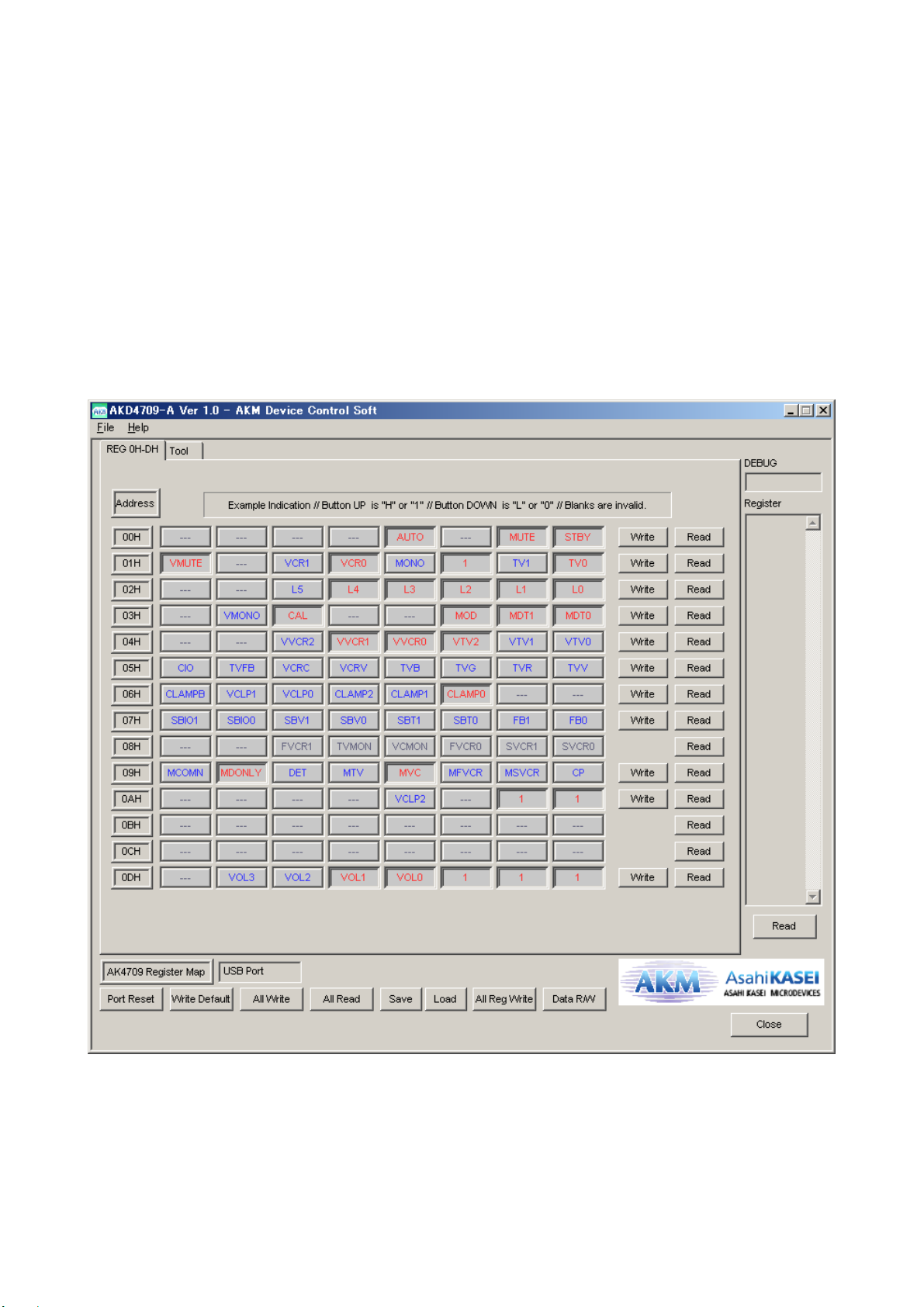
Jumper pins set up
[JP1] (GND): AINL- pin input select
OPEN: J20 (AINL): 3pin <Default>
SHORT: GND (Not use)
[JP2] (GND): AINR- pin input select
OPEN: J29 (AINR): 3pin <Default>
SHORT: GND (Not use)
[JP3] (VCRRC): VCRRC pin input select
I: J30 (VCRRC) <Default>
I/O: J23 (VCRCOUT)
[JP4] (GND): Analog ground and Digital ground
OPEN: Separated
SHORT: Common. (The connector “DGND” can be open.) <Default>
[JP5] (VD1): Regulator +3.3V or VD1 connector
- 2 -

ASAHI KASEI [AKD4709-A]
<KM103002> 2011/06
OPEN: VD1 pin is supplied from VD1 connector.
SHORT: VD1 pin is supplied to regulator +3.3V. (The connector “VD1” can be open.) <Default>
[JP7] (VCC): VVD connector or VCC connector
OPEN: Logic voltage is supplied from VCC connector.
SHORT: Logic voltage is supplied form VVD connector. (The connector “VCC” can be open.) <Default>
[JP8] (VVD): VD1 connector or VVD connector
OPEN: VVD1 and VVD2 pins are supplied from VVD connector.
SHORT: VVD1 and VVD2 pins are supplied from VD connector.
(The connector “VVD” can be open.) <Default>
The regulator can be supplied 3.3V to all circuits by shorting JP5, JP7 and JP8 and supplying 12V to VP connector.
The function of the toggle SW
[SW1] (PDN): Resets the AK4709. Keep “H” during normal operation.
The indication content for INT pin
Changes of the 08H status can be monitored via the TEST1 (INT). The INT pin is the open drain output and goes “L” for
2μs (typ.) when the status of 08H is changed.
Serial Control
The AK4709 can be controlled via the printer port (parallel port) of IBM-AT compatible PC. Connect PORT1 (CTRL)
with PC by 10-line flat cable packed with the AKD4709-A. The control software packed with this evaluation board
supports I2C control only.
Connect
ACK
SCL
SDA
10pin Header
10pin
Connector
10 wire
flat cable
PC AKD4708-A
Figure 2. Connect of 10-line flat cable
AKD4709-A
- 3 -

ASAHI KASEI [AKD4709-A]
<KM103002> 2011/06
Analog Input/Output List
Signal Name Note
J3 (VCRINL), J7 (VCRINR), J11 (TVINL), J15 (TVINR) Max. 2Vrms
Input J19 (AINL+), J27 (AINR+)
J20 (AINL+, AINL-), J27 (AINR+, AINR-), Max. 2Vrms
Audio
Output J4 (TVOUTL), J8 (TVOUTR), J12 (VCROUTL),
J12 (VCROUTR) Max. 2.15Vrms
Input
J1 (ENCV), J5 (ENCY), J9 (ENCRC), J13 (ENCC), J17 (ENCG)
J22 (ENCB), J25 (TVVIN), J28 (VCRVIN), J30 (VCRRC)
J31 (VCRG), J33 (VCRB)
Max. 1.25Vpp
Video
Output J2 (TVVOUT), J6 (TVRC), J10 (TVG), J14 (TVB)
J18 (VCRVOUT), J23 (VCRCOUT) Max. 2.5Vpp
Input J26 (VCRSB) Max. VP+0.3VSlow
Blanking Output J24 (TVSB), J26 (VCRSB) Max. VP
Input J32 (VCRFB) Max. VVD1+0.3VFast
Blanking Output J21 (TVFB) Max. VVD2
Table 1. Analog Input/Output List
- 4 -

ASAHI KASEI [AKD4709-A]
<KM103002> 2011/06
Control Soft Manual
■Evaluation Board and Control Soft Settings
1. Set an evaluation board properly.
2. Connect the evaluation board to an IBM PC/AT compatible PC by a 10wire flat cable. Be aware of the direction of
the 10pin header. When running this control soft on the Windows 2000/XP, the driver which is included in the CD
must be installed. Refer to the “Driver Control Install Manual for AKM Device Control Software” for installing the
driver. When running this control soft on the windows 95/98/ME, driver installing is not necessary. This control soft
does not support the Windows NT.
3. Proceed evaluation by following the process below.
■Operation Screen
1. Start up the control program following the process above.
The operation screen is shown below.
- 5 -

ASAHI KASEI [AKD4709-A]
<KM103002> 2011/06
■Operation Overview
Function, register map and testing tool can be controlled by this control soft. These controls are selected by upper tabs.
Buttons which are frequently used such as register initializing button “Write Default”, are located outside of the switching
tab window. Refer to the “■Dialog Boxes” for details of each dialog box setting.
1. [Port Reset]: For when connecting to USB I/F board (AKDUSBIF-A)
Click this button after the control soft starts up when connecting USB I/F board (AKDUSBIF-A).
2. [Write Default]: Register Initializing
When the device is reset by a hardware reset, use this button to initialize the registers.
3. [All Write]: Executing write commands for all registers displayed.
4. [All Read]: Executing read commands for all registers displayed.
5. [Save]: Saving current register settings to a file.
6. [Load]: Executing data write from a saved file.
7. [All Reg Write]: [All Reg Write] dialog box is popped up.
8. [Data R/W]: [Data R/W] dialog box is popped up.
9. [Read]: Reading current register settings and display on to the Register area (on the right of the main window).
This is different from [All Read] button, it does not reflect to a register map, only displaying
hexadecimal.
- 6 -

ASAHI KASEI [AKD4709-A]
<KM103002> 2011/06
■Tab Functions
[REG 0H~DH]: Register Map
This tab is for a register writing and reading.
Each bit on the register map is a push-button switch.
Button Down indicates “H” or “1” and the bit name is in red (when read only it is in deep red).
Button Up indicates “L” or “0” and the bit name is in blue (when read only it is in gray)
Grayout registers are [Read Only] registers. They can not be controlled.
The registers which is not defined in the datasheet are indicated as “---”.
- 7 -

ASAHI KASEI [AKD4709-A]
<KM103002> 2011/06
[Write]: Data Writing Dialog
It is for when changing two or more bits on the same address at the same time.
Click [Write] button located on the right of the each corresponded address for a pop-up dialog box.
When checking the checkbox, the register will be “H” or “1”, when not checking the register will be “L” or ”0”.
Click [OK] to write setting value to the registers, or click [Cancel] to cancel this setting.
[Read]: Data Read
Click [Read] button located on the right of the each corresponded address to execute register reading.
After register reading, the display will be updated regarding to the register status.
Button Down indicates “H” or “1” and the bit name is in red (when read only it is in deep red).
Button Up indicates “L” or “0” and the bit name is in blue (when read only it is in gray)
Please be aware that button statuses will be changed by Read command.
- 8 -

ASAHI KASEI [AKD4709-A]
<KM103002> 2011/06
[Tool]: Testing Tools
This tab screen is for evaluation testing tool.
Click buttons for each testing tool.
- 9 -

ASAHI KASEI [AKD4709-A]
<KM103002> 2011/06
■Dialog Boxes
1. [All Req Write]: All Req Write dialog box
Click [All Reg Write] button in the main window to open register setting files.
Register setting files saved by [SAVE] button can be applied.
[Open (left)]: Selecting a register setting file (*.akr).
[Write]: Executing register writing.
[Write All]: Executing all register writings.
Writings are executed in descending order.
[Help]: Help window is popped up.
[Save]: Saving the register setting file assignment. The file name is “*.mar”.
[Open (right)]: Opening a saved register setting file assignment “*. mar”.
[Close]: Closing the dialog box and finish the process.
*Operating Suggestions
(1) Those files saved by [Save] button and opened by [Open] button on the right of the dialog “*.mar” should be
stored in the same folder.
(2) When register settings are changed by [Save] button in the main window, re-read the file to reflect new register
settings.
- 10 -

ASAHI KASEI [AKD4709-A]
<KM103002> 2011/06
2. [Data R/W]: Data R/W Dialog Box
Click the [Data R/W] button in the main window for data read/write dialog box.
Data write is available to specified address.
Address Box: Input data address in hexadecimal numbers for data writing.
Data Box: Input data in hexadecimal numbers.
Mask Box: Input mask data in hexadecimal numbers.
This is “AND” processed input data.
[Write]: Writing to the address specified by “Address” box.
[Read]: Reading from the address specified by “Address” box.
The result will be shown in the Read Data Box in hexadecimal numbers.
[Close]: Closing the dialog box and finish the process.
Data writing can be cancelled by this button instead of [Write] button.
*The register map will be updated after executing [Write] or [Read] commands.
- 11 -

ASAHI KASEI [AKD4709-A]
<KM103002> 2011/06
MEASUREMENT RESULTS
Audio
[Measurement condition]
•Measurement unit : Audio Precision SYS-2722
•BW :20Hz∼20kHz
•Power Supply : VP=12V, VD1=3.3V, VD2=3.3V, VDD1=3.3V, VDD2=3.3V
•Interface : Input: Cannon, Output: BNC
•Temperature : Room
•Volume#0 Gain : 0dB
•Measurement signal line path: AINL/AINR →Volume#0 →Volume#1 →TVOUTL/TVOUTR
Parameter Input signal Measurement filter Results
Lch [dB]
Results
Rch [dB]
S/(N+D)
(At 2Vrms Output)
1kHz, 0dBFS 20kLPF 95.0 94.9
DR 1kHz, -60dBFS 22kLPF, A-weighted 99.0 99.2
S/N “no-input 22kLPF, A-weighted 99.0 99.2
Plots
Figure 1-1. FFT (1kHz, 0dBFS input) at 2Vrms output
Figure 1-2. FFT (1kHz, -60dBFS input)
Figure 1-3. FFT (Noise floor)
Figure 1-4. THD+N vs. Input Level (fin=1kHz)
Figure 1-5. THD+N vs. fin (Input Level=0dBFS)
Figure 1-6. Linearity (fin=1kHz)
Figure 1-7. Frequency Response (Input Level=0dBFS)
Figure 1-8. Crosstalk (Input Level=0dBFS)
- 12 -

ASAHI KASEI [AKD4709-A]
<KM103002> 2011/06
Video
[Measurement condition]
•Signal Generator : Sony Tectronix TG2000
•Measurement unit : Sony Tectronix VM700T
•Power Supply : VP=12V, VD1=3.3V, VD2=3.3V, VDD1=3.3V, VDD2=3.3V
•Interface : Input: BNC, Output: BNC
•Temperature : Room
•Measurement signal line path: S/N: ENCV →TVVOUT
Y/C Crosstalk: ENCV →TVVOUT, ENCRC →TVRC
DG, DP: ENCV →TVVOUT
Parameter Input Signal Measurement Filter Results Unit
S/N 0% Flat Field BW=15kHz to 5MHz
Filter=Uni-Weighted
76.2 dB
Y/C Crosstalk
(Measured at TVVOUT)
100% Red Field
(YÆENCV, CÆENCRC)
BW=15kHz to Full -59.5
(Note1)
dB
DG Modulated 5 step Min: -0.36
Max: 0.00
%
DP Modulated 5 step Min: -0.95
Max: 0.28
deg.
Plots
Figure 2-1. Noise spectrum (Input=0% Flat Field, BW=15kHz to 5MHz, Filter=Uni-Weighted)
Figure 2-2. Y/C Crosstalk (Measured at TVVOUT, Input= 100% Red, ENCV=Y, ENCRC=C), BW=15kHz to Full)
Figure 2-3. DG, DP (Input= Modulated 5 step)
(Note1) Y/C Crosstalk: Reference Measurement: Results: 1.7dB (p-p)
Composite signalÆENCV, no inputÆENCRC, TVRC is terminated by 75Ohm.
Y/C Crosstalk: Measurement: Results: -57.8dB (p-p)
YÆENCV, CÆENCRC, TVRC is terminated by 75Ohm.
Y/C Crosstalk calculation: -57.8dB (p-p) – 1.7dB (p-p) = -59.5dB (p-p)
- 13 -

ASAHI KASEI [AKD4709-A]
<KM103002> 2011/06
Plots (Audio)
AK4709 AINL/AINR ÆTVOUTL/TVOUTR: FFT: fin=1KHz, Input Level=0dB
-180
+0
-170
-160
-150
-140
-130
-120
-110
-100
-90
-80
-70
-60
-50
-40
-30
-20
-10
d
B
r
A
20 20k50 100 200 500 1k 2k 5k 10k
Hz
Figure1-1. FFT (fin=1kHz, Input Level=0dB)
AK4709 AINL/AINR ÆTVOUTL/TVOUTR: FFT: fin=1KHz, Input Level=-60dB
-180
+0
-170
-160
-150
-140
-130
-120
-110
-100
-90
-80
-70
-60
-50
-40
-30
-20
-10
d
B
r
A
20 20k50 100 200 500 1k 2k 5k 10k
Hz
Figure-1-2. FFT (fin=1kHz Input Level=-60dB)
- 14 -

ASAHI KASEI [AKD4709-A]
<KM103002> 2011/06
AK4709 AINL/AINR ÆTVOUTL/TVOUTR: FFT: No-input
-180
+0
-170
-160
-150
-140
-130
-120
-110
-100
-90
-80
-70
-60
-50
-40
-30
-20
-10
d
B
r
A
20 20k50 100 200 500 1k 2k 5k 10k
Hz
Figure1-3. FFT (Noise Floor)
AK4709 AINL/AINR ÆTVOUTL/TVOUTR: THD+N Amplitude vs Input Amplitude: fin=1KHz
-110
-80
-108
-106
-104
-102
-100
-98
-96
-94
-92
-90
-88
-86
-84
-82
d
B
r
A
-140 +0-130 -120 -110 -100 -90 -80 -70 -60 -50 -40 -30 -20 -10
dBr
Figure1-4. THD+N vs. Input level (fin=1kHz)
- 15 -

ASAHI KASEI [AKD4709-A]
<KM103002> 2011/06
AK4709 AINL/AINR ÆTVOUTL/TVOUTR: THD+N Amplitude vs Input Frequency: Input Level=0dB
-110
-80
-108
-106
-104
-102
-100
-98
-96
-94
-92
-90
-88
-86
-84
-82
d
B
r
A
20 20k50 100 200 500 1k 2k 5k 10k
Hz
Figure1-5. THD+N vs. Input Frequency (Input level=0dB)
AK4709 AINL/AINR ÆTVOUTL/TVOUTR: Linearity: fin=1KHz
-140
+0
-130
-120
-110
-100
-90
-80
-70
-60
-50
-40
-30
-20
-10
d
B
r
A
-140 +0-130 -120 -110 -100 -90 -80 -70 -60 -50 -40 -30 -20 -10
dBr
Figure1-6.Linearity (fin=1kHz)
- 16 -

ASAHI KASEI [AKD4709-A]
<KM103002> 2011/06
AK4709 AINL/AINR ÆTVOUTL/TVOUTR: Frequency Response: Input Level=0dBr
-3
+1
-2.8
-2.6
-2.4
-2.2
-2
-1.8
-1.6
-1.4
-1.2
-1
-0.8
-0.6
-0.4
-0.2
+0
+0.2
+0.4
+0.6
+0.8
d
B
r
A
20 20k50 100 200 500 1k 2k 5k 10k
Hz
Figure1-7. Frequency Response (Input level=0dB)
AK4709 AINL/AINR ÆTVOUTL/TVOUTR: Crosstalk: fin=1KHz, Input Level=0dBr / No-input
-140
-70
-135
-130
-125
-120
-115
-110
-105
-100
-95
-90
-85
-80
-75
d
B
20 20k50 100 200 500 1k 2k 5k 10k
Hz
TTTTTT
Figure1-8. Crosstalk (Input level=0dB)
- 17 -

ASAHI KASEI [AKD4709-A]
<KM103002> 2011/06
Plots(Video)
AK4709 ENCV ÆTVVOUT: S/N: Input Signal=0% Flat Field, BW=15kHz to 5MHz, Filter=Uni-Weighted
Figure 2-1. Noise spectrum (Input=0% Flat Field, BW=15kHz to 5MHz, Filter=Uni-Weighted)
- 18 -

ASAHI KASEI [AKD4709-A]
<KM103002> 2011/06
AK4709 ENCV ÆTVVOUT / ENCRCÆTVRC: Y/C Crosstalk: Input Signal=100% Red Field,
YÆENCV, CÆENCRC, BW=15kHz to Full
Figure 2-2 Crosstalk (Measured at TVVOUT, Input= 100% Red Field, YÆENCV, CÆENCRC, BW=15kHz to Full)
- 19 -

ASAHI KASEI [AKD4709-A]
<KM103002> 2011/06
AK4709 ENCV ÆTVVOUT: DG, DP: Input Signal=Modulated 5 step
Figure 2-3 DG, DP (Input Signal= Modulated 5 step)
- 20 -
Table of contents
Other Asahi KASEI Motherboard manuals

Asahi KASEI
Asahi KASEI AKD5538-B User manual

Asahi KASEI
Asahi KASEI AKD2300 User manual

Asahi KASEI
Asahi KASEI AKM AKD5538-B User manual

Asahi KASEI
Asahi KASEI AK5704 User manual

Asahi KASEI
Asahi KASEI AKD4220-A User manual

Asahi KASEI
Asahi KASEI AKD4382A-SB User manual

Asahi KASEI
Asahi KASEI AK9720 Installation instructions

Asahi KASEI
Asahi KASEI AKD4140-B User manual