Avago ADNK-3043-ND24 Guide

ADNK-3043-ND24
2.4GHz RF Wireless USB Optical Mouse Designer’s Kit
Design Guide
Introduction
This design guide describes the design of a low power
consumption optical mouse using the Texas Instrument
MSP430F1222 microcontroller, the Avago ADNS-3040
optical sensor and a Nordic nRF2402 2.4 GHz transmit-
ter. The receiver dongle is implemented with a Nordic
nRF2401 in conjunction with a Cypress CY7C63231 USB
controller. The document discusses the reference design
hardware and the rmware implementation. Included
in Appendix A is the schematic for this reference design
mouse. The software section of this document describes
the architecture of the rmware required to implement
the mouse functions. The MSP430F1222 data sheet is
available on the TI web site at www.ti.com. The ADNS-
3040 data sheet is available from the Avago web site at
www.avagotech.com. USB controller data sheet can be
found on the Cypress web site: www.cypress.com. The
Nordic transmitter and receiver data sheets are available
on www.nordicsemi.no
Key reference design objectives:
1. Highlight the low-power benet of the ADNS-3040
2. Demonstrate a design with a RF daughter board to
facilitate experimentation with dierent RF technolo-
gies
3. Feature a Flash-based development environment to
facilitate rapid rmware changes
Features
•Complete LED mouse reference design kit
•Windows® 98SE, Windows 2000 and Windows XP
compatibility
•USB 1.0 low-speed compliance
•User identity code to avoid conict with other de-
vices
•High reliability
•Smooth surface navigation
•Enhanced SmartSpeed self-adjusting frame rate for
optimum performance
•High speed motion detection up to 20 ips and 8 G
•800 cpi resolution
•No mechanical moving parts
•A high data rate 2.4GHz RF link
•Transmission data rate up to 1Mbps
•15 meters communication distance
•Self-adjusting power-saving modes for longest bat-
tery life
•Minimal number of passive components

2
RF Board
Left Button
Avago
ADNS-3040
Optical Mouse
Sensor
Wheel Button
Right Button
Z Optics
TI
MSP430F1222
Microcontroller
MISO
MOSI
SCLK
NCS
Control
and Data
MAX1722
Boost Regulator
Quadrature
Signals
Lens
Image
Array
LED
Lens
Surface
Shadow pattern
Figure 2. Illustration of Optical Navigation technology
Reference Design Overview
The image-based optical mouse sensor takes snap shots
of the surface it is navigating on. It measures changes in
position by comparing the sequential images (frames) and
mathematically determines the direction and magnitude
of movement. The traditional duel-channel optical
encoder generates the quadrature Z-wheel movement
signals. This design guide illustrates the hardware con-
nection of a LED-based optical mouse with standard con-
guration; as well as the rmware management and the
handling of the USB protocols. USB protocol provides a
standard way of reporting mouse movement and button
presses to the PC. The Windows HID driver interprets the
USB data and performs the cursor movements and mouse
clicks.
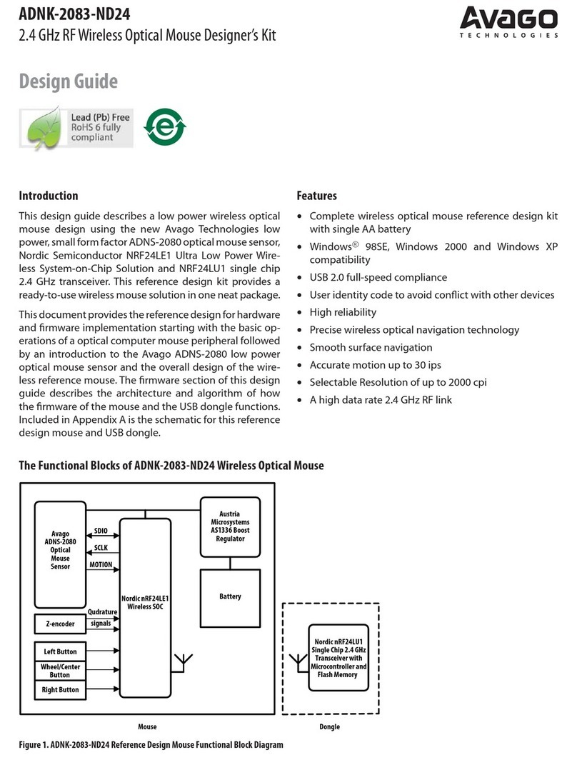
The functional block diagram of the reference design
mouse is shown in Figure 1. The optical sensor detects
the X and Y movements. An optical quadrature encoder
provides the Z-wheel movement. Each of the button
switches is pulled up normally and provides a Ground
when pressed. The MAX1722 boost regulator maintains
the 2.7 V operating voltage for the reference design
mouse from two regular AA Alkaline batteries in parallel.
Theory of Operation
Navigation Technology
The heart of the ADNS-3040 navigation sensor is a CMOS
image array. An LED and an optical system illuminate
the surface that the ADNS-3040 is navigating on. The
texture of the surface casts bright and dark spots forming
distinct images as the sensor is moved across the surface.
A Digital Signal Processing (DSP) engine and its built-in
algorithm evaluate these images and determine the
magnitude and direction of the movement. The motion
data is made available in the delta_X and delta_Y registers
for the system controller to retrieve. An extensive power
saving topology is implemented within the ADNS-3040
navigation engine. A Motion pin (output) is available to
act as the system interrupt. As long as there is no motion
the system can remain in Sleep mode allowing maximum
battery power saving. Based on the last detected motion
the ADNS-3040 navigation engine enters various power
saving modes when no new motion occurs. These power
saving features make the ADNS-3040 ideally for wireless
applications.
Figure 1. ADNK-3043-ND24 Reference Design Mouse functional Block Diagram

3
Z-Wheel
The motion of Z-wheel is detected using the quadrature
signal generated by optical sensors. Two phototransistors
are connected in a source-follower conguration forming
Channel A and Channel B. An infrared LED shines,
causing the phototransistors to turn on. In between the
phototransistors and LED is a pinwheel that turns on the
mouse ball rollers. The fan of this pinwheel is mechanical-
ly designed to block the infrared light such that the pho-
totransistors are turned on and o in a quadrature output
pattern. Every change in the phototransistor outputs rep-
resents a count of mouse movement. Comparing the last
state of the optics to the current state derives directional
information. As shown in Figure 3. below, rotating the
wheel forward produces a unique set of state transitions,
and rotating the wheel backward produces another set of
unique state transitions.
Figure 3. Optics Quadrature Signal Generation
Mouse Buttons
Mouse buttons are connected as standard switches. These
switches are pulled up by the pull up resistors inside the
microcontroller. When the user presses a button, the
switch will be closed and the pin will be pulled LOW to
GND. A LOW state at the pin is interpreted as the button
being pressed. A HIGH state is interpreted as the button
has been released or the button is not being pressed.
Normally the switches are debounced in rmware for 15-
20ms. In this reference design there are three switches:
left, Z-wheel, and right.
Hardware Implementation
Optical Mouse Sensor
This reference design features the ADNS-3040 optical
navigation engine. It contains an Image Acquisition System
(IAS), a Digital Signal Processor (DSP), and a three-wire
Serial Peripheral Interface consists of the serial clock (SCLK),
the master-in/slave-out (MISO) and the master-out/slave-
in (MOSI). In addition a fourth signal, Motion, is an output
intended to act as an interrupt to the microcontroller
whenever the ADNS-3040 senses motion. When the mouse
is moved the ADNS-3040 alerts the system controller by
activating the Motion signal triggering an interrupt service
routine. At the same time the ADNS-3040 accumulates
the horizontal and vertical displacements (count per inch,
or cpi) in its Delta_X and Delta_Y registers respectively.
The ADNS-3040 deactivates the Motion signal as soon as
movement stops. The SmartSpeed technology automati-
cally optimizes the frame rate by examining the acquired
images of the surface. It also manages the integrated LED
driver to coordinate with the shutter.
The system controller reads the motion information and
reports it to the PC to update the cursor position.
The advantages of using ADNS-3040 optical sensor are the
ecient power management, high tracking accuracy, and
ecient communications with the optical sensor via the
full duplex SPI port.
To learn more about sensor’s technical information, please
visit the Avago web site at http://www.avagotech.com
Microcontroller
The Texas Instruments MSP430 family of ultra-low power
microcontrollers consists of several devices featuring
dierent sets of peripherals targeted for various applica-
tions. The architecture, combined with ve low-power
modes, is optimized to achieve extended battery life in
portable measurement applications. The device features
a powerful 16-bit RISC CPU, 16-bit registers, and constant
generators that attribute to maximum code eciency. The
Digitally Controlled Oscillator (DCO) allows wake-up from
low-power modes to active mode in less than 6 µsec.
The specic device used in this reference design is the
MSP430F1222 with 28 pin to accommodate ample amount
of I/O. It is an ultra-low power mixed-signal microcontrol-
lers with a built-in 16-bit timer, 10-bit A/D converter with
integrated reference and Data Transfer Controller (DTC),
and 14 (20 pin package) or 22 (28 pin package) general
purpose I/O pins. The MSP430x12x2 series microcontrol-
lers have built-in communication capability using asyn-
chronous (UART) and synchronous (SPI) protocols.
4
frequency synthesizer, a power amplier, a crystal oscilla-
tor and a modulator. The output power and channel are
programmed through the SPI. Chip Select (CS) is used to
enable the nRF2402 when the microcontroller is ready
to pass it the motion or button switch data. Once the
data has been loaded into its input buer the nRF2402
manages the transmission and returns to power down
mode to conserve battery power. Typical power consump-
tion is 10 mA at -5 dBm of output power.
The nRF2402 has two transmit modes:
•ShockBurstTM
•Direct Mode
In this reference design ShockBurstTM is used to capital-
ize on its benet. It utilizes the on-chip FIFO to accept SPI
data at the microcontroller operating rate but transmit at
very high rate (up to 1 Mbps). The short transmission time
enables extreme power saving. For detailed description
of the ShockBurstTM technology please refer to: www.
nordicsemi.no/
High-frequency PCB layout:
A well-designed PCB is necessary to achieve good RF
performance. A fully qualied RF layout for the nRF2402
and it’s surrounding components, including matching
networks for the antenna can be downloaded from:
www.nordicsemi.no
A PCB with a minimum of two layers including a ground
plane is recommended for optimum performance.
The nRF2402 dc supply should be well filtered and
decoupled as close as possible to the Vdd pins with high
performance RF capacitors. Specically a high-grade
SMD tantalum capacitor (e.g. 4.7 µF) should be used in
parallel with the smaller-value high-frequency bypassing
capacitors. The nRF2402 should have its own branch of
well-ltered supply voltage, routed separately from the
supply voltage for the digital circuitry.
Full swing digital signals should not be routed close to the
crystal or the power supply lines.
Serial Peripheral Interface (SPI)
The MSP430F1222 provides a dedicated hardware-based
Serial Peripheral Interface (SPI). The three-wire interface
supports byte serial communication in either Master or
Slave mode. In this reference design the MSP430F1222
always acts as the master and initiates all SPI communi-
cations with external SPI device(s), in this case the ADNS-
3040 and the nRF2401.
Z-Wheel Quadrature Encoder
A standard two-channel, incremental optical quadrature
encoder and an IR LED provide the scroll wheel function.
The MSP430F1222 manages the IR LED directly. Since
achieving low-power consumption is one of the main ob-
jectives, the optical LED is only enabled when the MSP430
needs to read the output states of the optical quadrature
encoder to the MSP430 port pins while in ACTIVE mode.
The optical LED is pulsed on for approximately 40 µsec
every 2 msec while in ACTIVE mode to read the current
position of the scroll wheel, thus saving power since the
optical LED is only on for a duty cycle of 2%. The outputs
of the two-channel quadrature encoder are squarewaves
that are 90° out of phase. The phase relationship of these
signals encodes the directions of scroll wheel rotations.
Within the MSP430, an internal Quadrature Encoder Pulse
(QEP) state machine interprets these signals and incre-
ments or decrements a counter based on the direction
and movement of the scroll wheel.
Wireless RF Technology
In order to provide the maximum exibility the reference
design mouse utilizes two circuit boards. The main board
consists of the ADNS-3040 navigation sensor/LED, the
MSP430F1222 microcontroller, the scroll wheel and
button switches. A 10-pin header connects the main
board to the RF daughter card. The Nordic nRF2401 2.4
GHz transmitter and its associated circuit including the
antenna resides on the daughter card. The 10-pin header
provides the SPI, regulated Vdd and unregulated battery
voltage (for possible future applications). The nRF2402 is
a single-chip transmitter for the world wide 2.4-2.5 GHz
ISM band. The transmitter consists of a fully integrated

5
HLMP-ED80-PS000 (LED)
ADNS-2220-001
ADNS-3040
Customer supplied
ADNS-3120-001
Customer supplied base
plate with recommended
alignment features per
IGES drawing
Caution: The lens is not permanently attached to the sensor and will drop out of the assembly.
Some details on ADNK-3043-ND24
The ADNK-3034-ND24 reference design kit allows users
to evaluate the performance of the Optical Tracking
Engine (sensor, lens, LED assembly clip, LED) over a RF
connection. This kit also enables users to understand the
recommended mechanical assembly. (See Appendix C,
D, and E)
System Requirements
PCs using Windows95/ Windows98/ WindowsNT/
Windows2000 with standard 3-button USB mouse
driver loaded.
Functionality
This reference design is an optical mouse with three
buttons and a scroll wheel.
USB Operating Mode
The receiver dongle is hot pluggable into the USB port.
The PC does not need to be powered o when plugging
or unplugging the receiver dongle for the evaluation
mouse.
Figure 4. Exploded view of the ADNS-3040 optical tracking engine
Sensor
Object Surface
Lens
2.55
0.10
Figure 5. Distance from lens reference plane to surface
To Disassemble the ADNK-3043-ND24 Unit
The ADNK-3034-ND24 comprises of the plastic mouse
casing, a main printed circuit board (PCB), lens, buttons,
and a 2.4 GHz RF daughter card, and a 2.4 GHz USB
receiver dongle. (See Figure 4.) Removing the screws
located at the base of the unit separate the top and the
bottom of the mouse casing. Removing the PCB assembly
from the base plate further disassembles the mouse unit.
Be careful with the battery terminals while separating the
PCB assembly with the bottom casing.
While reassembling the components, please make sure
that the Z height (Distance from lens reference plane to
surface) is maintain. Refer to Figure 5.

6
Regulatory Requirements
•Passes FCC B and worldwide analogous emission
limits when assembled into a mouse with unshielded
cable and following Avago recommendations.
•Passes EN61000-4-4/IEC801-4 EFT tests when as-
sembled into a mouse with unshielded cable and fol-
lowing Avago recommendations.
•UL ammability level UL94 V-0.
•Provides sucient ESD creepage/clearance distance
to avoid discharge up to 15kV when assembled into a
mouse according to usage instructions above.
•For eye safety consideration, please refer to the docu-
ment, Eye Safety Calculation AN1228 available on the
web site, http://www.avagotech.com/opticalnaviga-
tion
Below is the summary of the components contained in
the ADNK-3034-ND24 Designer’s Kit.
Sensor
The sensor technical information is contained in the
ADNS-3040 Data Sheet.
Other system components
Technical information on the TI MSP430F1222 microcon-
troller is contained in the TI Data Sheet. Please contact
your local TI oce for theMSP430 development tools.
These tools will allow the designer to make changes and
recompile the source code; perform In-Circuit Emulation
and debug new code for added features.
Programming support and programmer adaptors for the
MSP430 can be found through TI or through other 3rd
party programming tool companies. For further informa-
tion on this product, please contact Texas Instrument.
Cypress Semiconductor provides extensive develop-
ment tools for the CY7C63231 USB controller used in the
receiver dongle.
Lens
The lens technical information is contained in the ADNS-
3120-001 Data Sheet.
LED Assembly Clip
The information on the assembly clip is contained in the
ADNS-2200 Data Sheet.
LED
The LED technical information is contained in the HLMP-
ED80-PS000 Data Sheet and Application Note AN-1228.
Additional application notes regarding Eye Safety Re-
quirements are also available at Avago’s website.
Base Plate Feature – IGES File
The IGES le on the CD-ROM provides recommended
base plate molding features to ensure optical alignment.
This includes PCB assembly diagrams like solder xture in
assembly and exploded view, as well as solder plate. See
Appendix D for details.
Reference Design Documentation – Gerber File
The Gerber File presents detailed schematics used in
ADNK-3034-ND24 in PCB layout form. See Appendix C
for more details.
Overall circuit
A schematic of the overall circuit is shown in Appendix A
of this document. Appendix B lists the bill of materials.

7
Figure 6. Reference Design Mouse Software Architecture
CPU Main Processing Loop
(1) Process MOTION data
(2) Process BINDING packet
(3) Process BUTTON data
(4) Update SCROLL WHEEL
QEP state machine
(5) Send out WHEEL position
(if changed since last check)
(6) If 10 mins inactivity, go into
DEEP SLEEP mode, else
repeat loop
Sensor
MOTION
Port 2
Interrupt
Transmitter Module
(1) Build raw data packet
(2) Submit packet to Tx queue
(3) Turn RF transmitter ON
(3) Shift data out serially according to Miller
encoding scheme
(4) Turn RF transmitter OFF
LEFT Button
Port 1 Interrupt
PORT 1 Interrupt
Service Routine
WHEEL Button
Port 1 Interrupt
RIGHT Button
Port 1 Interrupt
Scroll Wheel Module
(1) Turn Wheel LED ON
(2) Read scroll wheel position
(3) Turn Wheel LED OFF
(4) Update QEP state machine
CONNECT Button
Port 2 Interrupt
PORT 2 Interrupt
Service Routine
Periodic
TIMER_A1
Interrupt
(every 2 msec)
TIMER_A0 Interval Interrupt
WatchDog Interval Interrupt
(every 250 milliseconds)
WDT Interrupt Service Routine
(1) Trigger WHEEL position check
(2) Decrement Timeout counter
Firmware Implementation
The rmware for this reference design is written in the C language.
The following les are required to compile the mouse rmware.
•MSP430_AVAGO_ADNS-3040.c – main mouse rmware
•CRC-8.c – Routines for CRC-8 generation
•wm430_buttons.c – used to store button state data for tx message
•wm430_system.c
•wm430_transmitter.c – mplements the RF transmitter protocol
•wm430_wheel.c – Implements the logic to detect scroll wheel movement
•_FSKDATAPLUSENCODING – used to enable MSP430 to shift data out via FSK scheme by toggling the
RF_DATA line at specic bit periods
The user should insert the receiver dongle into an available USB port at the computer. Install two AA alkaline batteries
into the battery compartment. Pay special attention to the polarities of the two batteries. The reference design mouse
is designed to work with two AA batteries in parallel or just one AA battery. Press the connect button on the receiver
dongle and while the LEDs are ashing press the connect button at the underside of the mouse. When the mouse is
properly “connected” to the dongle every time it receives a transmission from the mouse the green LED lights up.

8
Appendix A: Schematic Diagram of the Main Board
Figure A1. Schematic Diagram of Sensor and Microcontroller main Board
Vdd
Binding
Left_SW
Z_SW
Right_SW
13
11
9
7
5
3
12
4
6
8
10
12
14
Vdd
GND
GND
2
4
7
25
26
27
28
1
5
6
18
16
15
3
Control 3
Binding
Vdd
11
10
24
23
22
21
20
19
9
8
14
12
13
17
Vdd
Vdd
Z_SW
Right_SW
Left_SW
Z_En
Vdd
Z_En
Vdd
J105
JTAG
MMBT3906LT1
Q101R124
10k
R125
240
D103
MIE-114A1
E
BC
2
1
3
C112
Vdd
U104
QA
QB
MID-95A3LH
0.1uF
R108 R107
27k 27k
R105
105k
MPS430F1222IPW
32.768kHz
XTAL101
Vdd
Vss
RST/NMI
P1.4
P1.5
P1.6
P1.7
TST
XOUT
XIN
P3.7
P3.5
P3.4
P2.5
U102
P3.0
P2.2
P1.3
P1.2
P1.1
P1.0
P2.4
P2.3
P2.1
P2.0
P3.3
P3.1
P3.2
P3.6
R104
100k
C101
0.01uF
0.1uF
C102
GND
VBATT
Vdd
T101
Battery spring
Battery spring+ Battery spring-
T102 T103
JP1
C103
10uF
1
2
3 4
5
BATT
GND
FB
U103
LX
OUT
JP2
10uH
L101
R109
1.1M
R110
1.0M
C104
10uF
HLMP-ED80
D102
R111
10
C107
1uF
C108
0.01uF
MISO
MOSI
SCLK
Vdd
C105 1uF
C106 0.01uF
MAX1722
R122
Open
10
5
1
3
4
2
11
19
14
9
SHTDWN
MOTION
NCS
SCLK
MOSI
MISO
AVDD
AGND
AGND
AGND
XY_LED
LED_GND
NC
NC
NC
NC
VDD
GND
GND
GND
ADNS-3040
6
7
20
18
17
8
15
16
13
12
C109
1uF
C110
0.01uF
Control 1
Control 2
Vdd
GND
Control 3
SCLK
MOSI
MISO
NC
VBatt
1 2
3 4
5 6
7 8
910
Header
J101
SW101
SW102
SW103
SW104
Connect
Left
Scroll
Right
R101
100k
R102 R103
100k 100k

9
Figure A2. Schematic Diagram of RF Transmitter Daughter Board
Vdd Vdd/
Vdd/
Control1
Control2
MOSI
SCLK
NCS/
Vdd/
VBatt
NC
MISO
MOSI
SCLK
NCS/
GND
Vdd
16
15
14
13
12
11
10
9
8
7
6
5
4
3
2
1
Vss_PA
ANT1
ANT2
Vdd_PA
Vdd
IREF
Vss
PWR_UP
CE
CS
CLK
DIN
Vdd
XC1
XC2
Vss
R202
22K
C211
2.2nF
C212
22pF
22nH
L203
3.6nHL201
1pF
C202
1pF
C201
C213
1.5pF
Antenna
R203
5C210
10uF
C205 C206
1nF 10nF
22pF C208 C207
22pF
X20116MHz
R201
1M
U201
nRF2402
1 2
34
5 6
78
910

10
Figure A3. Schematic Diagram of USB Dongle
C10
4.7uF
VDD3V3
1
2
3
4
J101
CON4
C302
100nF
C301
100nF
VDD3V3
IN 1
ON/OFF 3
OUT
5
NC
4
GND
2
U300
LP2980IM5-3,3 USB5V
C2
15pF
0603
C5
1nF
0603
C6
10nF
0603
R2
22K
0603
C4
2.2nF
0603
VDD3V3
xxx
xxx
xxx
C1
15pF
0603
R1
1M
X1
16 MHz
XC1
XC2
C3
22pF
PWR_UP-3V
CE-3V
DR2-3V
CLK2-3V
DOUT2-3V
CS-3V
DR1-3V
CLK1-3V
DATA-3V
C7
33nF
PWR_UP-5V
USBDP
USBDN
P0.0
1
P0.1
2
P0.2
3
P0.3
4
P1.0
5
Vss
6
Vpp
7
Vreg/P2.0
8
P2.1
9P2.2 10
Vcc 11
D- 12
D+ 13
P1.1 14
P0.7 15
P0.6 16
P0.5 17
P0.4 18
U100
CY7C63231A
USB5V
D101
Green
DOUT2-5V
CLK2-5V
DR2-5V
CE-5V
CS-5V
DR1-5V
CLK1-5V
DATA-5V
LED
C110
10nF
+ C109
4,7uF
R110
1.3k
Vreg
R21033k
R21133k
R21233k
R21333k
R21433k
R21533k
R21633k
R21733k
R21833k
R20922k
R20822k
R20722k
R20622k
R20522k
R20422k
R20322k
R20222k
R20122k
R111
150ohm
L1
3.3nH
L2
10nH
C8
1.0pF
C9
1.0pF C12
2.2pF
L3
5.6nH
L4
5.6nH
C11
4.7pF
CE
1
VDD 24
VSS 18
VDD 17
VSS_PA 16
DR2
2
CLK2
3
DOUT2
4
CS
5
DR1
6
CLK1
7
DATA
8
DVDD
9
VSS
10
XC2
11
XC1
12
ANT2 15
ANT1 14
VDD_PA 13
IREF 19
VSS 20
VDD 21
VSS 22
PWR_UP 23
nRF2401A
U1
NRF2401A

11
Appendix B: Bill of Materials (BOM)
Table B1. BOM for Components Shown on Schematic: Sensor and Microcontroller Main Board
Part Type Value Quantity Designators
Optical Sensor Device 1 U101
Optical Sensor LED 1 D102
Optical Sensor Lens 1 Not shown on schematic
Optical Sensor Clip 1 Not shown on schematic
Microcontroller 1 U102
DC/DC Converter 1 U103
Z LED 1 D103
Z Encoder 3 PIN 1 U104
Resistor (0805) 100 k 5 R101, R102, R103, R104, R105
Resistor (0805) 3.3M 1 R124
Resistor (0805) 240 1 R125
Resistor (0805) 27K 2 R107, R108
Resistor (0805) 1.1 M 1 R109
Resistor (0805) 1.0 M 1 R110
Resistor (0805) 10 1 R111
Resistor (0805) 0 1 R106
Resistor (0805) No Load 1 R122
Ceremic capacitor (0603) .01UF 50V 4 C101, C106, C108, C110
Ceremic capacitor (0603) .1UF 25V 2 C102, C112
Tantalum capacitor 1 uF 50V 3 C105, C107, C109
Tantalum capacitor 10uF 25V 2 C103, C104
NPN T RANSISTOR MMBT3906LT1 1 Q101
Switch SPDT 3 SW101, SW102, SW103
Switch, light touch 1 SW104
Inductor 10 uH 1 L101
Crystal 32.768 kHz 1 XTAL101
Header, pins 2mm 2x5 2 J101
Header, socket, 2mm 2 x 7 2 J105
Battery Spring, common 2X7 1 T101
Battery spring + 1 T102
Battery spring - 1 T103

12
Part Description Value Quantity Reference
Resistor (0402) 22k 1 R202
Resistor (0402) 5.1 1 R203
Resistor (0402) 1 M 1 R201
Ceramic Capacitor, 50v X7R (0402) 1nF 1 C205
Ceramic Capacitor, 50v X7R (0402) 10nF 1 C206
Ceramic Capacitor, 50v NPO (0402) 1.5pF 1 C213
Ceramic Capacitor, 50V. NPO (0402) 1pF 2 C201, C202
Ceramic Capacitor, 50v NPO (0402) 22pF 3 C208, C207,C212
Ceramic Capacitor, 50v X7R (0402) 2.2 nF 1 C211
Ceramic Capacitor, 50V. X7R (0402) 10uF 1 C210
Inductor 3.6 nH 1 L201
Inductor 22 nH 1 L203
nRF2402 nRF2402 U201
10-PIN Header 2x5 pin, 1mm pitch (M) 1 P201
Crystal, Ceramic, Model 405 16 MHz (M1) 1 X201
BOM for nRF2402 Reference Design: RF Board
Table B2. BOM for Components Shown on Schematic: RF Transmitter Daughter Board
*Note: Must be programmed before assembly

13
Part Description Value Quantity Designator
Capacitor (C0G (NP0), 50 V, ±5 %, 0603) 15pF 2 C1,C2
Capacitor (C0G (NP0), 50 V, ±5 %, 0603) 22pF 1 C3
Capacitor (X7R, 16 V, ±10 %, 0603) 2.2nF 1 C4
Capacitor (X7R, 16 V, ±10 %, 0603) 1nF 1 C5
Capacitor (X7R, 16 V, ±10 %, 0603) 10nF 1 C6
Capacitor (X7R, 16 V, ±10 %, 0603) 33nF 1 C7
Capacitor (±0.1pF, 50 V, NPO, 0603) 1.0pF 1 C8, C9
Tantal Capacitor (10uF ±20%, 3216) 4.7uF 2 C10, C109
Capacitor (C0G (NP0), 50 V, ±5 %, 0603) 4.7pF 1 C11
Capacitor (±0.1pF, 50 V, NPO, 0603) 2.2pF 1 C12
Capacitor (X7R, 16 V, ±10 %, 0603) 10nF 1 C110
Capacitor (X7R, 16 V, ±10 %, 0603) 100nF 2 C301,C302
LED (1206) Green 1 D101
ACON USB Plug (Freber: FCMP04208) CON4 1 J101
Panasonic ELJRE3N3ZF2 3.3nH 1 L1
Panasonic ELJRE10NJF2 10nH 1 L2
Panasonic ELJRE5N6JF2 5.6nH 1 L3
Panasonic ELJRE5N6JF2 5.6nH 1 L4
Resistor (0.1W, 1%, 0603) 1M 1 R1
Resistor (0.1W, 1%, 0603) 22K 1 R2
Resistor (0.1W, 1%, 0603) 1.3k 1 R110
Resistor (0.1W, 1%, 0603) 150 1 R111
Resistor (0.1W, 1%, 0603) 22k 9 R201, R202, R203,
R204, R205, R206,
R207, R208, R209
Resistor (0.1W, 1%, 0603) 33k 8 R210, R211, R212,
R213, R214, R215,
R216, R21, R218
Nordic Semiconductor Transceiver nRF2401A 1 U1
Cypress USB Controller* CY7C63231A 1 U100
3.3V Regulator LP2980IM5-3,3 1 U300
Crsytal (LxWxH = 4.0x2.5x0.8, Cl=9pF, tol + drift =30 ppm) 16 MHz 1 X1
Table B3. BOM for Components Shown on Schematic: USB Dongle

14
Appendix C: Base Plate Feature
Figure C1. Illustration of base plate mounting features
ADNS
DIMENSIONS:
31.5 x 17.0 mm
ADNS-3120-001 LEN RECESS
DIMENSIONS:
31.5 x 17.0 mm
KEY PYRAMID
FEATURE:
2.50mm HEIGHT MAX.
KEY PYRAMID
FEATURE:
2.50mm HEIGHT MAX.

Appendix D: Sectional view of PCB assembly
PCB
Sensor
LED
Base Plate
Lens/Light Pipe
Clip
Surface
Appendix E: Receiver dongle Implementation
The USB receiver dongle for this reference design is supplied by Nordic Semiconductor. The following Nordic applica-
tion note details the hardware design and rmware implementation. The application note can be downloaded from:
www.nordicsemi.no
Universal low cost USB DuoCeiverTM nAN24-04 using nRF2401TM
Figure E1. low cost USB DuoCeiverTM
Figure E1: Sectional view of PCB assembly highlighting all optical mouse components
(optical mouse sensor, clip, lens, LED, PCB, and base plate).

16
Ordering Information
For ordering information, please contact your local Avago sales representative.
Part Number Description Name Quantity
ADNK-3043-ND24
Mouse Set
a. Wireless LED Mouseb. USB
Dongle
Reference Design Mouse Set 1
ADNS-3040 LED Mouse Sensor Sensor 5
ADNS-3120-001 LED Mouse Trim Lens Plate Lens 5
ADNS-2220 LED Clip LED Clip 5
HLMP-ED80-PS000 Light Emitting diode LED 5
ADNK-3043-ND24
CD
Includes Documentation and Support Files for ADNK-3043-ND24
Documentation
a. ADNS-3040 Ultra Low Power Optical Mouse Data Sheet
b. ADNK-3043-ND24 Optical Mouse Designer’s Kit Product Overview
c. ADNK-3043-ND24 Optical Mouse Designer’s Kit Design Guide
d. Avago ADNS-3120-001 Solid State Optical Mouse Lens datasheet
e. Battery Life Calculation for an Ultra Low Power Wireless Optical
Mouse Application Note 5243
f. Texas Instrument MSP430F1222 Microcontroller Datasheet
g. Nordic Semiconductor nRF2401A RF Transceiver Datasheet
h. Nordic Semiconductor nRF2402 RF Transmitter Datasheet
Hardware Support Files
a. ADNK-3043-ND24 BOM List
b. ADNK-3043-ND24 Schematic
c. ADNK-3043-ND24 Gerber File
d. IGES Base Plate Feature File
Software Support Files
a. Microcontroller Firmware
1
For product information and a complete list of distributors, please go to our web site: www.avagotech.com
Avago, AvagoTechnologies, and the A logo are trademarks of Avago Technologies, Limited in the United States and other countries.
Data subject to change. Copyright © 2007 Avago Technologies Limited. All rights reserved.
AV02-0193EN - March 15, 2007
Appendix F: Kit Components
The designer’s kit contains components as follows:
www.nordicsemi.com
Nordic Semiconductor Support
Tel: +47 72 89 89 00
www.nordicsemi.no/sup_com/pro.php
www.ti.com
TI Semiconductor Product Information Center
support.ti.com
www.morrihan.com.cn
Morrihan International
Trading (Shanghai) Co., Ltd
Tel : +86 21 58369345
Avago Technologies’ Partners
For partner product information and list of distributors, please go to their respective website.
Table of contents
Other Avago Mouse manuals

Avago
Avago ADNK-5703 Guide

Avago
Avago LaserStream ADNK-6093-SP11 Guide

Avago
Avago ADNK-6003-SP01 Guide

Avago
Avago ADNK-2703 Guide

Avago
Avago ADNK-3083 Guide

Avago
Avago ADNK-6013-SP01 Guide

Avago
Avago ADNK-5023-HTP2 Guide

Avago
Avago ADNK-5033-CSBT Guide

Avago
Avago ADNK-2083-ND24 User manual

Avago
Avago ADNK-5003 Guide