Barton Musical Circuits BMC58 User manual
BMC58. Yes No Maybe Sequencer
last updated August 28th, 2019
I. Using The Module
A. Wha does his do?
B. Con rols
C. Changing Modes
II. Schema ic
A. Mas er Schema ic
B. Swi ches
C.Inpu s
D.Ou pu s
III. Cons ruc ion
A.Par s Lis
B.PCB Informa ion
C.Wiring
I.Using The Module
A. Wha does i do?
This sequencer outputs an 8 or 16 step pattern. Each step has a toggle that can set the output
definitely on ( ES), definitely off (NO) or maybe on or off (MA BE). The probability of an
output being on can be controlled with the MA BE knob and MA BE CV input.
It has three modes: 1 channel 16 steps long with gate and trigger outputs, 2 channels 8 steps
long with trigger outputs or 2 channels 8 steps long with gate outputs.
B. Con rols/IO
1.Toggles – There are 16 toggles, each corresponding to a single step of the sequence. When
a toggle is pushed to the left (NO), there is no output on that step. When pushed to the right ( ES)
an output will always fire on that step. When the toggle is centered (MA BE), the output will
sometimes fire with the probability controleld by the MA BE knob.
2.MA BE knob – This knob controls the probability of the MA BE steps firing. When fully
counterclockwise no MA BE steps will fire and when fully clockwise all MA BE steps will fire.
3.MA BE CV knob/input – The Maybe CV is attenuated by the CV knob and then mixed
with the voltage from the MA BE knob. A negative voltage inputted will act like turning the
MA BE knob counterclockwise and a positive will act like turning the knob clockwise.
4.Reset Button/input – The Reset button returns the sequence to step one on the next clock
input. It is also used for selecting modes at power up, so it's a good idea to not leave something
patched to the Reset input when first powering up as it could accidentally cause an accidental mode
change.
5.Clock input – This is a clock for the sequencer.
6.Outputs – The two outputs will output a trigger or gate signal with a range of 0 to +5V.
The type of output is controlled by what mode the sequencer is in.
C.Changing Modes
1. With the module powered down, set the knob's position to the selected mode.
2. Hold down the reset button.
3. Power up the module without releasing the reset button.
MODE # of channels Outputs Knob position
16 Step 1 1x Gate, 1x Trigger Fully Clockwise
8 Step G 2 2x Gate Centered (up)
8 Step T 2 2x Trigger Fully
Counterclockwise

II. Schema ic
A. Mas er Schema ic
Above is the master schematic. It comprises both PCBs. The components on the Top PCB
have a blue background and the components on the bottom PCB have a yellow background.
On the next pages, I'll show different sections of the project in easier to follow bits. ou may
notice that the master schematic shows a 10K
resistor bus, in the following schematics, these
will be shown as 10K resistors.
On the right is an image of the pinout of
the PIC.
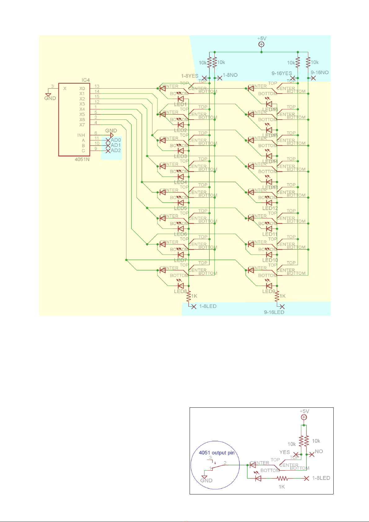
B. Swi ches
Above are the toggles, LEDs and the circuitry that controls it. On the far left of the image is
the CD4051 CMOS switch. Pins 9, 10 and 11 of this are connected to the PIC, which controls
which of the output pins connects to ground.
Each output pin is connected to two LEDs and two switching diodes connected to the center
of an ON/OFF/ON SPDT toggle. Steps 1 and 9 are both connected to the same output pin of the
4051 as are 2 and 10, etc.
The two outside lugs of each toggle are connected to the PIC with a 10K pull-up resistor set
to +5V. When the CD4051 connects to ground for that switch, if the toggle connects the PIC to
ground through the switch and diode, it tells the
PIC whether or not to fire the output for that step.
The anodes of the LEDs are connected to a
pin on the PIC through a 1K current limiting
resistor. When the LED controlling pin goes to
+5V, the LED will light up for the current step.
To the right is a simplified version of a
single toggle/LED set for clarity. The 4051 output
pin is represented as a switch.

C.Inpu s
To the right are the
inputs for the module. On
the top left, we see the
Maybe and Maybe CV
pots. The voltage on the
wipers of these pots is
mixed together by the
TL072 op amps and 100K
resistor network. Before
connecting to the CV input
pin of the PIC, a 1K
resistor and a pair of
schottky diodes form a
voltage limiting circuit,
and a .01uf capacitor
filters noise.
Under the CV
inputs are the clock and
reset inputs. Each of these
is connected to an opamp on the TL074. The opamps are wired as comparators with their thresholds
set at .5V by the 10K/1K voltage divider. Each comparator has a 100K resistor to ground on it's
input, and it's output goes through a switching diode to prevent negative voltage passing from the
comparator's output to the PIC's inputs. A 100K/100K voltage divider and a schottky diode
connected to +5V prevent overvoltage from damaging the PIC's input pins.
D.Ou pu s
Above are the outputs. The opamps are wired as non-inverting buffers. They connect to
LEDs through a 1K current limiting resistor, to the output wirepads through a 1K output impedance
setting resistor.

III. Cons ruc ion
A.Par s Lis
Semiconductors
Value Qty Notes
PIC16f685 1 Came with your PCB
TL072 1 8 pin DIP package
TL074 1 14 pin DIP package
CD4051 1 16 pin DIP package
78L05 1 +5V voltage regulator, TO92 package
Schottky Diode 4 Any schottky diode should work, 1N5819, 1N60, BAT46, etc
Switching Diode 19 1N4148, 1N914 or any small signal switching diode
LED 18 3mm package
Resistors
Value Qty Notes
10 ohm 2 7.5mm lead spacing. 1/4w Metal Film unless otherwise noted on all
resistors
1K ohm 8
100K ohm 11
10K 6 pin bussed
array
1 SIP package, or make your own.
B100K Pot 2 PC mounted 9mm, parallel mount. Like this.
Capacitors
Value Qty Notes
.01uf 6 Ceramic type. Value not critical.
10uf 2 2.5mm lead spacing Electrolytic 16V or higher
Other
Value Qty Notes
8 pin DIP socket 1
14 pin Dip socket 1
16 pin DIP socket 1
20 pin DIP socket 1
Power Connecter 1 either Eurorack or MOTM style, depending on your synth format
SPDT ON-OFF-
ON
16 I use these. They will fit the PCB
Jack 5 Whatever type your synth format uses
Pushbutton 1 I use these. They will fit the PCB
2x8 Female Pin 1 I uses these.

Header
2x8 Male Pin
Header
1 I buy 40 pin two row male header like this, and then cut it down.
B. PCB Informa ion
To the right are images of the
bottom and top of the bottom PCB
and the top of the top PCB.
C.Wiring
Wiring is very simple. The CLOCK,
TRIG, RES, GATE and CVIN
wirepads all connect to the tip of the
appropriate jack. GND connects to
the sleeve of a single jack if using a
metal panel. If using a
nonconductive panel, connect it to
the sleeve of each jack.
On the next pages are photos of a
completed build.

Here is a complete build using a home made resistor array.

Above is a close up of jack wiring. I used clipped resistor leads instead of wires to save on wire.
Above is a close up of the connection between the two PCBs. Make sure you clip leads on the
bottom side of the top PCB so they don't short against the 4051 that sits below the PCB. There are
holes in the PCB to use an optional spacer to keep PCBs seperated.
Table of contents
Other Barton Musical Circuits Recording Equipment manuals


