Barton Musical Circuits Chordizer User manual

BMC052. Chordizer
Last updated 8-27-2017
If you have any questions, or need help trouble shooting, please e-mail
Mi hael@Bartonmusi al ir uits. om
I Overview/Controls/Inputs/Outputs
II Schematic
III Construction
A. arts List
B.The CB
C.Wiring
D.Callibration

I. Overview/Controls/Inputs/Outputs
A. Overview – The goal of the Chordizer was to use a single voltage input and output a quantized
hord of voltages when used with 1v/o tave VCOs. A voltage is inputted through the IN ja k and
an be modulated by the AUX ja k and it's asso iated attenuator. The voltage range for the input is
0 to 5V.
Offsets to the input voltage are then applied, these offsets are ontrolled by three pots and
an be negative or positive offsets. When the offset voltage is outside of the voltage range of the
module, it will be transposed down or up an o tave automati ally to put it ba k into the voltage
range.
The input voltage and the offset voltages are then quantized. The QUANT knob sele ts what
musi al s ale is used to quantize. Before the voltage is finally output, a slew or portamento is
applied, ontrolled by the SLEW knob.
The module is ompatible with 12V or 15V systems without making any modifi ations. It
also has apabilities to have voltage ontrollable hord sele tion.
B.Controls -
1.OFFSET knobs – These knobs ontrol the offset of the voltages. They are numbered OFF1,
OFF2 and OFF3. When the knob is pointed straight up, no offset is applied. When turned lo kwise
the offset be omes more positive and when turned ounter lo kwise, the offset be omes more
negative. OFF1 ontrols the voltage outputted at the OUT2 ja k, OFF2 the OUT3 ja k and OFF3
the OUT4 ja k.
2.AUX knob – This attenuates the voltage inputted at the CV ja k whi h is then mixed with the
voltage from the IN ja k.
3.CHORD knob – This knob sele ts the memory bank to use in SAVE or LOAD operations. There
are 8 memory banks total. The knob attenuates the input of the CHORD ja k, whi h is normalized
to +5V when nothing is plugged into it. When using a 0 to 5V range sequen er to sele t hords,
leave this knob fully lo kwise.
4.QUANT knob – This sele ts what s ale is used in quantization. The table below outlines the
s ales. They are presented in order of least lo kwise to most lo kwise when rotating the knob.
SCALE root b2nd 2nd b3rd 3rd 4th b5th 5th b6th 6th b7th 7th
Chromati ON ON ON ON ON ON ON ON ON ON ON ON
Major ON off ON off ON ON off ON off ON off ON
Minor ON off ON ON off ON off ON ON off ON off
Harmoni Minor ON off ON ON off ON off ON ON off off ON
Major Pentatoni ON off ON off ON off off ON off ON off off
Minor Pentatoni ON off off ON off ON off ON off off ON off
O tave and 5ths ON off off off off off off ON off off off off
O tave ON off off off off off off off off off off off
5.SLEW knob – This knob ontrols how mu h the notes slew from one to another.
6.TUNE toggle – When a tivated this sets all outputs to 1V so os illators an be tuned together.
7.5ths toggle – When a tive OUT2 will always be a 5th above the input voltage.
8.Quantize-Then-Offset toggle – When a tive, the input voltage will be quantized before offsets
are applied. This makes so that smaller hanges in input voltage do not hange the output.
9.SELECT toggle – This toggle ontrols how the SELECT button and input work. When in the
enter position it will sele t a hord at random. When in the up position it will rotate through the
saved hords in as ending order and in the down position will rotate in des ending order.

10.SAVE button – When pressed this will save the urrent offsets to the memory bank sele ted by
the CHORD knob.
11.LOAD button – When pressed or when the LOAD input goes high, this will load offsets from
the sele ted memory bank. Adjusting an OFFSET knob will override the loaded offset for that
output.
12.SELECT button – When pressed or when the SELECT input goes high, this will load a saved
hord using the logi determined by the SELECT toggle.
IN UTS
1. MAIN Input – This is the main input, it is mixed with the AUX input and it's quantized output
appears at the OUT1 ja k.
2. AUX input – This is an auxiliary input ja k. The voltage is attenuated by the AUX ja k and then
mixed with the MAIN input.
3.TRACK input – This input is normalized to +5V when nothing is plugged in. When this input
goes low (voltage is less than 0V) the module will ignore hanges from the MAIN and AUX
voltages.
4.LOAD input – This initiates a load like hitting the LOAD button.
5.SELECT input – This initiates a sele t like hitting the SELECT button.
OUT UTS
1-4. VOLTAGE OU UTS – The only outputs are the 4 quantized voltage outputs. OUT1
orresponds to the input, OUT2 orresponds to the input offset by OFF1, OUT3 orresponds to the
input offset by OFF2 and OUT4 orresponds to the input offset by OFF3.
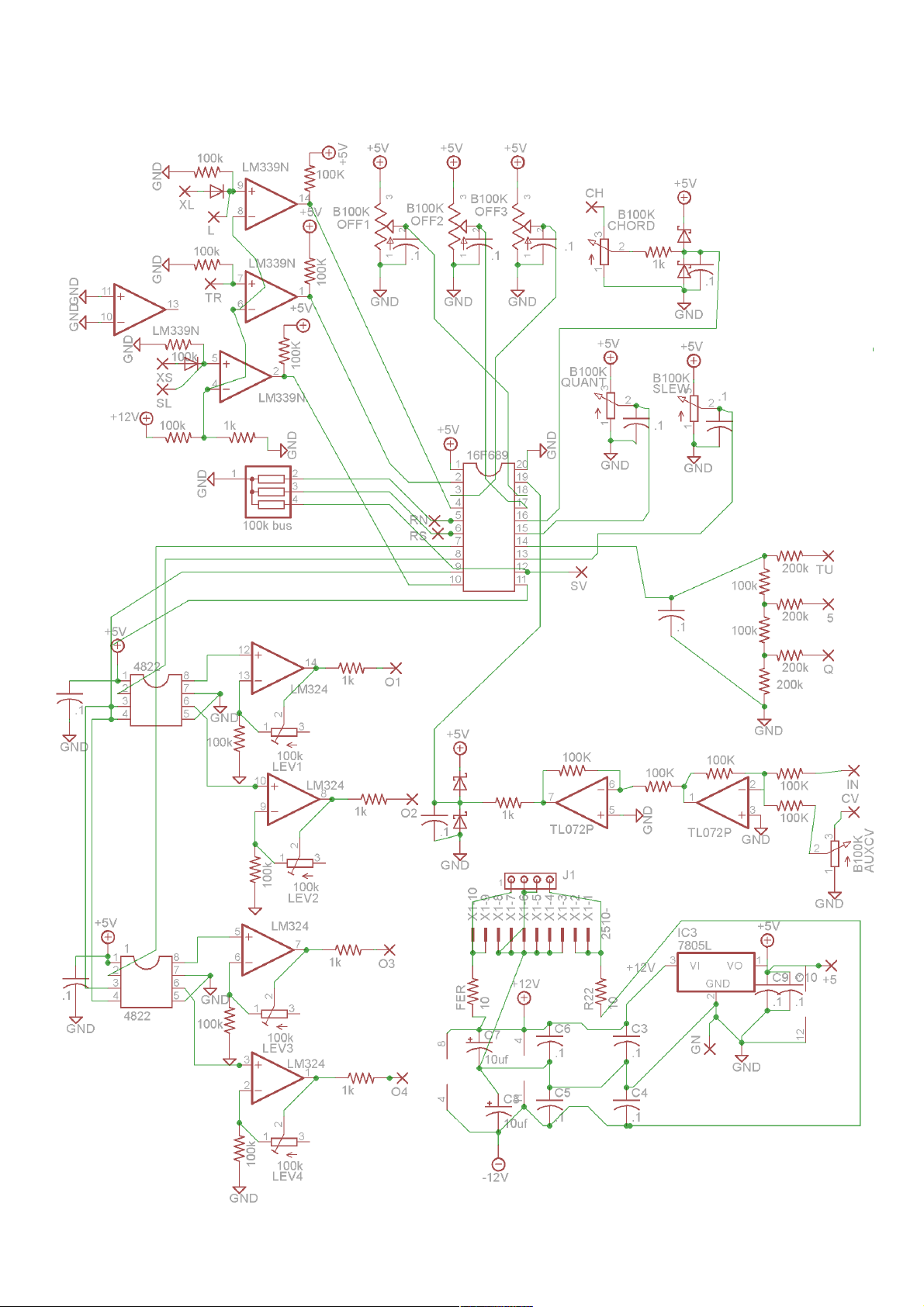
II. Schematic.

On the previous page is the s hemati for this
module's printed ir uit board. At the enter is the 16F689
PIC mi ro ontroller. The pinout for the hip is presented to
the right. The Sele t toggle and Save button wirepads are
onne ted dire tly to the pins of the PIC and pull down
resistors from a 100K resistor bus.
At the top left of the s hemati we see the gates of
an LM339 omparator hip. The omparators threshold are
set by the 100K/1K voltage divider whi h is onne ted to
the negative input of ea h omparator. This sets the threshold at .012V when using a 12V power
supply. The positive inputs of the omparators are ea h onne ted to a 100K pull down resistor
whi h brings the input to 0V when nothing is input and then the wirepads for the buttons and
swit hing diodes onne ting to the external inputs for the Load, Tra k and Sele t ja ks. The outputs
of the omparators are onne ted to 100K pull up resistors to +5V and then to the pins of the PIC.
To the right of the omparators are the potentiometers for the various ontrol knobs other
than the AUX knob. All of these are set up identi ally as variable voltage dividers between 0V and
5V. The wiper of ea h pot is onne ted to a apa itor to filter high frequen y noise out and then to
the pin of the PIC, other than the CHORD knob. The CHORD knob's wiper is onne ted to a 1K
resistor and a pair of S hottky diodes whi h form a voltage limiting ir uit that limit the voltage to
between 0V and 5V.
To the right of the PIC in the s hemati we see the wirepads of the toggle swit hes and some
resistors. Ea h toggle wirepad will be at either 0V or +5V, and this resistor network (known as a
R/2R ladder) onverts the toggle positions to a single voltage. This allows us to read several toggles
with a single pin of the PIC.
Below the toggle inputs are the main CV input and AUX input ir uit. The voltages from the
input and Aux CV are mixed together by an inverting op-amp and then inverted ba k to their
original voltage by a se ond inverting op-amp. The output of the se ond op-amp goes through the
same voltage limiting network as the CHORD knob and is then sent to the PIC.
In the bottom left are the output ir uitry. Two MCP4822 Digital-To-Analog onverter ICs
are used. Ea h hip is onne ted to the serial digital output (SDO) and serial lo k (SCK) pins of
the PIC, and then to a hip sele t pin. Ea h hip has two analog outputs. These outputs are sent to a
non-inverting op-amp gain stage with a trimpot in it's feedba k path. The trimpots are adjusted
during alibration to ensure a urate tuning.
In the bottom right is the power onne tions/filtering. Footprints for a Eurora k and MOTM
style power onne ter are in parallel with ea h other. The voltage rails are filtered by a 10ohm
resistor and 10uf passive low pass filter. The LM324 quad op amp and the TL072 Dual op amp are
onne ted to the power rails and have small apa itors next to their power pins to filter out high
frequen y digital noise. A 7805L voltage regulator provides the 5V power supply for the
MCP4822s, the LM339 omparators and the 16F689 PIC.
III. Construction
A. arts List
Semiconductors
Name Quantity Notes
16F689 1 Should be provided with your PCB
LM324 1 14 pin DIP pa kage
TL072 1 8 pin DIP pa kage
LM339 1 14 pin DIP pa kage
4822 DAC 2 8 pin DIP pa kage
Swit hing diode 2 1N4148 or other small signal swit hing diode
S hottky diode 4 BAT46 or other s hottky
78L05 Regulator 1 TO 92 pa kage
Resistors
Name/Value Quantity Notes
10 ohm 2 1/4w metal Film for all resistors unless otherwise noted
1K ohm 7
100K ohm 19
200K ohm 4
100K ohm buss 1 4pin SIP pa kage. Or an be made with 3 resistors*
B100K Pots PC Mounted 4 16 mm Alpha linear taper, PC Mounted. Like this.
B100K Pots Solder Lug 3
100K Cermet trimmer 4 3296 pa kage
* http://www.bartonmusicalcircuits.com/makearray.html
Capacitors
Name/Value Quantity Notes
.01uf 16 Cerami dis . Value not riti al
10uf 2 Ele trolyti , at least 16V rating.
Other
Name/Value Quantity Notes
Power onne ter 1 Eurora k or MOTM
Pushbutton 3 OFF-(ON). Like this.
ON-ON Toggle swit h 3 SPDT. Like this.
On-Off-On Toggle swit h 1 SPDT. Like this.
Swit hing Ja k 2
Mono Ja k 8 Swit hing ja k will work as mono ja k

Knobs 7
20 pin DIP so ket 1
14 pin DIP so ket 2
8 pin DIP so ket 3
B. The CB
The PCB is 93x60mm. The mounting holes are spa ed 51.1mm apart and pots are spa ed 25.4mm
apart. Below is an image of the PCB
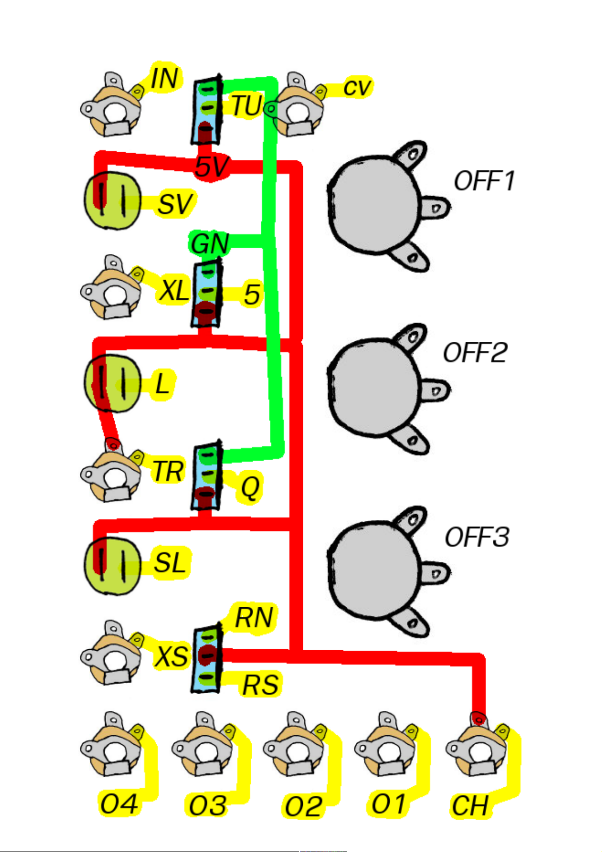
C.Wiring
On the next page is a wiring diagram. I suggest wiring the 5V bus (in red on the diagram)
between the swit hes and ja ks first, then the ground bus (in green). If you are using a ondu tive
front panel and ja ks with ondu tive sleeves, you only need to wire ground to the sleeve of one
ja k as shown. If using a non- ondu tive panel or non- ondu tive ja k sleeves, you should ground
all ja ks.
Next, I would wire the offset pots, and then wire the rest going from one end of the PCB to
the other.

D. Calibration
1.A tivate the Tune knob.
2.Adjust the trimpot for ea h hannel until the output voltage of that hannel is exa tly 1V.
3.If your meter has low resolution, turn the SCALE knob fully lo kwise to OCTAVES mode.
4.Input a 5V signal and turn the offset knobs to 12 O Clo k.
5.Adjust the trimpots so that ea h hannel is at 5V.
This manual suits for next models
1
Other Barton Musical Circuits Recording Equipment manuals


