BBK DV985S User manual

SERVICE MANUAL
DV985S

CONTENTS
SAFETY PRECAUTIONS 1
PREVENTION OF ELECTRO STATIC DISCHARGE(ESD)TO ELECTROSTATICALLY
SENSITIVE(ES)DEVICES 1
PREVERTION OF STATIC ELECTRICITY DISCHARGE 3
ASSEMBLING AND DISASSEMBLING THE MECHANISM UNIT 4
OPTICAL PICKUP UNIT EXPLOSED VIEW AND PART LIST 4
BRACKET EXPLOSED VIEW AND PART LIST 6
ELECTRICAL CONFIRMATION 8
VI DEO OUTPUT (LUMINANCE SIGNAL) CONFIRMATION 8
VI DEO OUTPUT(CHROMINANCE SIGNAL) CONFIRMATION 9
MPEG BOARD CHECK WAVEFORM 10
AM29LV160D 19
SCHEMATIC & PCB WIRING DIAGRAM 44
SPARE PARTS LIST
HY57V641620HG 24
CONTROL BUTTON LOCATIONS AND EXPLANATIONS 2
MISCELLANEOUS 7
MT1389
60
41
FLI2300 DIGITAL VIDEO CONVERTER DATE SHEET 11
SiI 164 PANELLINK TRANSMITTER
27

1.1 GENERAL GUIDELINES
1. When servicing, observe the original lead dress. if a short circuit is found, replace all parts which have
been overheated or damaged by the short circuit.
2. After servicing, see to it that all the protective devices such as insulation barrier, insulation papers
shields are properly installed.
3. After servicing, make the following leakage current checks to prevent the customer from being exposed
to shock hazards.
Some semiconductor(solid state)devices can be damaged easily by static electricity. Such components
commonly are called Electrostatically Sensitive(ES)Devices. Examples of typical ES devices are integrated
circuits and some field-effect transistors and semiconductor chip components. The following techniques
should be used to help reduce the incidence of component damage caused by electro static discharge(ESD).
1. Immediately before handling any semiconductor component or semiconductor-equipped assembly, drain
off any ESD on your body by touching a known earth ground. Alternatively, obtain and wear a commercially
availabel discharging ESD wrist strap, which should be removed for potential shock reasons prior to
applying power to the unit under test.
2. After removing an electrical assembly equipped with ES devices,place the assembly on a conductive
surface such as alminum foil, to prevent electrostatic charge buildup or exposure of the assembly.
3. Use only a grounded-tip soldering iron to solder or unsolder ES devices.
4. Use only an anti-static solder removal device. Some solder removal devices not classified as anti-static
(ESD protected)can generate electrical charge sufficient to damage ES devices.
5. Do not use freon-propelled chemicals. These can generate electrical charges sufficient to damage ES
devices.
6. Do not remove a replacement ES device from its protective package until immediately before you are
ready to install it.(Most replacement ES devices are packaged with leads electrically shorted together by
conductive foam, alminum foil or comparable conductive material).
7. Immediately before removing the protective material from the leads of a replacement ES device, touch
the protective material to the chassis or circuit assembly into which the device will be installed.
Caution
Be sure no power is applied to the chassis or circuit, and observe all other safety precautions.
8. Minimize bodily motions when handling unpackaged replacement ES devices. (Otherwise harmless motion
such as the brushing together of your clothes fabric or the lifting of your foot from a carpeted floor can
generate static electricity(ESD).
notice (1885x323x2 tiff)

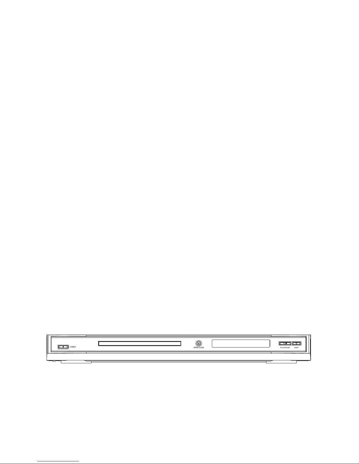
Front Panel Illustration
POWER switch
Disc tray
STOP button
IR SENSOR
Display window
OPEN/CLOSE button
6
5
4
2
3
7
2
7
6
PLAY/PAUSE button
345

The laser diode in the traverse unit (optical pickup)may brake down due to static electricity of clothes or human
body.Use due caution to electrostatic breakdown when servicing and handling the laser diode.
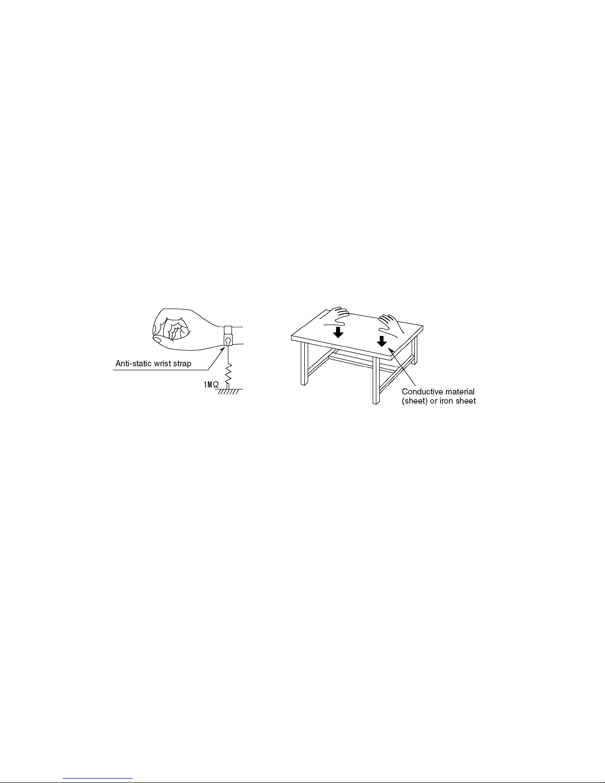
4.1.Grounding for electrostatic breakdown prevention
Some devices such as the DVD player use the optical pickup(laser diode)and the optical pickup will be damaged
by static electricity in the working environment.Proceed servicing works under the working environment where
grounding works is completed.
4.1.1. Worktable grounding
1. Put a conductive material(sheet)or iron sheet on the area where the optical pickup is placed,and ground the
4.1.2.Human body grounding
1 Use the anti-static wrist strap to discharge the static electricity from your body.
4.1.3.Handling of optical pickup
1. To keep the good quality of the optical pickup maintenance parts during transportation and before
installation, the both ends of the laser diode are short-circuited.After replacing the parts with new ones,
remove the short circuit according to the correct procedure. (See this Technical Guide).
2. Do not use a tester to check the laser diode for the optical pickup .Failure to do so willdamage the laser
diode due to the power supply in the tester.
4.2. Handling precautions for Traverse Unit (Optical Pickup)
1. Do not give a considerable shock to the traverse unit(optical pickup)as it has an extremely high-precise
structure.
2. When replacing the optical pickup, install the flexible cable and cut is short land with a nipper. See the
optical pickup replacement procedure in this Technical Guide. Before replacing the traverse unit, remove
the short pin for preventingstatic electricity and install a new unit.Connect the connector as short times as
possible.
3. The flexible cable may be cut off if an excessive force is applied to it.Use caution when handling the cable.
4. The half-fixed resistor for laser power adjustment cannot be adjusted. Do not turn the resistor.
safety_3 (1577x409x2 tiff)
sheet.

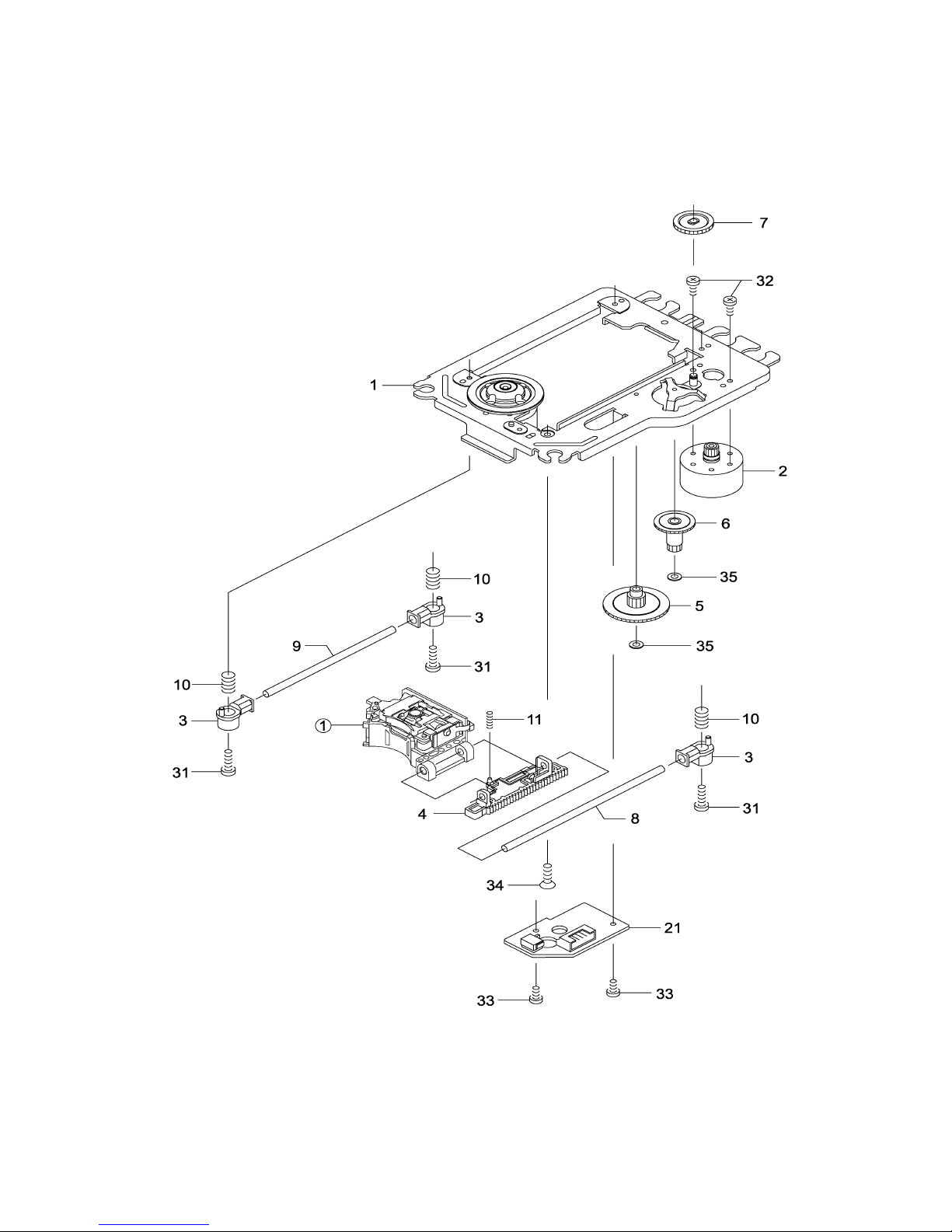
5.1 Optical pickup Unit Explosed View and Part List
Pic (1)

Materials to Pic (1)
No. PARTS CODE PARTS NAME Q ty
14692200 SF-HD60 1
1 1EA0311A06300 ASSY, CHASSIS, COMPLETE 1
2 1EA0M10A15500 ASSY, MOTOR, SLED 1
Or 1EA0M10A15501 ASSY, MOTOR, SLED 1
3 1EA2451A24700 HOLDER, SHAFT 3
4 1EA2511A29100 GEAR, RACK 1
5 1EA2511A29200 GEAR, DRIVE 1
6 1EA2511A29300 GEAR, MIDDLE, A 1
7 1EA2511A29400 GEAR, MIDDLE, B 1
8 1EA2744A03000 SHAFT, SLIDE 1
9 1EA2744A03100 SHAFT, SLIDE, SUB 1
10 1EA2812A15300 SPRING, COMP, TYOUSEI 3
11 1EA2812A15400 SPRING, COMP, RACK 1
21 1EA0B10B20100 ASSY, PWB 1
Or 1EA0B10B20200 ASSY, PWB 1
31 SEXEA25700--- SPECIAL SCREW BIN+-M2X11 3
32 SEXEA25900--- SPECIAL SCREW M1.7X2.2 2
33 SFBPN204R0SE- SCR S-TPG PAN 2X4 2
34 SFSFN266R0SE- SCR S-TPG FLT 2.6X6 1
35 SWXEA15400--- SPECIAL WASHER 1.8X4 X0.25 2
Note : This parts list is not for service parts supply.

5.2 Bracket Explosed View and Part List
Pic (2)
Materials to Pic(2)
1.bracket 14.frontsiliconrubber
2.belt15.Backsiliconrubber
3.screw 16.Pick-up
4.beltwheel 17.Pick-up
5.gearwheel 18.switch
6.ironchip 19.Five-pinflatplug
7. Immobility mechanism equipment 20. screw
8.Magnet 21.PCB
9.Platen 22.motor
10.Bridgebracket 23.Motorwheel
11.screw 24.screw
12.screw 25.tray
13. Big bracket
Before going process with disassembly and installation, please carefully both
peruse the chart and confirm the materials.

5.3 MISCELLANEOUS
5.3.1 Protection of the LD(Laser diode)
Short the parts of LD circuit pattern by soldering.
5.3.2 Cautions on assembly and adjustment
Make sure that the workbenches,jigs,tips,tips of soldering irons and measuring instruments are
grounded,and that personnel wear wrist straps for ground.
Open the LD short lands quickly with a soldering iron after a circuit is connected.
Keep the power source of the pick-up protected from internal and external sources of electrical
noise.
Refrain from operation and storage in atmospheres containing corrosive gases (such as H2S,SO2,
NO2 and Cl2)or toxic gases or in locations containing substances(especially from the organic silicon,cyan,
formalin and phenol groups)which emit toxic gases.It is particularly important to ensure that none of the
above substances are present inside the unit.Otherwise,the motor may no longer run.

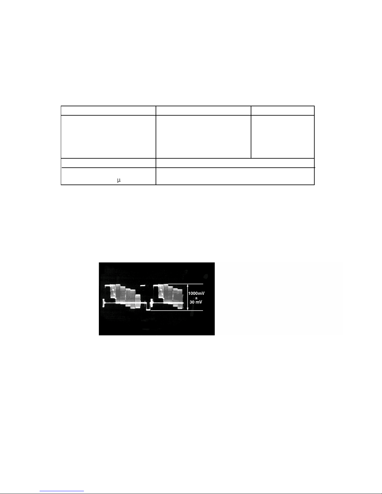
6.1. Video Output (Luminance Signal) Confirmation
DO this confirmation after replacing a P.C.B.
Purpose:To maintain video signal output compatibility.
1.Connect the oscilloscope to the video output terminal and terminate at 75 ohms.
2.Confirm that luminance signal(Y+S)level is 1000mVp-p±30mV
Measurement point
Video output terminal
Color bar 75%
PLAY(Title 46):DVDT-S15
PLAY(Title 12):DVDT-S01
DVDT-S15
or
DVDT-S01
Mode Disc
Measuring equipment,tools
200mV/dir,10 sec/dir 1000mVp-p±30mV
Confirmation value

Do the confirmation after replacing P.C.B.
Purpose:To maintain video signal output compatibility.
1.Connect the oscilloscope to the video output terminal and terminate at 75 ohme.
2.Confirm that the chrominance signal(C)level is 621 mVp-p±30mV
Measurement point
Video output terminal
Color bar 75%
PLAY(Title 46):DVDT-S15
PLAY(Title 12):DVDT-S01
DVDT-S15
or
DVDT-S01
Mode Disc
Measuring equipment,tools Confirmation value
Screwdriver,Oscilloscope
200mV/dir,10 sec/dir 621mVp-p±30mV


FLI2300 Digital Video Converter Data Sheet
*** Genesis Microchip Confidential ***
PRELIMINARY INFORMATION -- SUBJECT TO CHANGE
1 DESCRIPTION
The FLI2300 is a highly integrated digital video
format converter for CRT-TV applications using
patented deinterlacing and post processing algorithms
from Faroudja Laboratories, coupled with highly
flexible scaling, a wide variety of aspect ratio
conversions, and other special video enhancing
features to produce the highest quality image.
1.1 Inputs
• Input all industry standard and non-standard
video resolutions, including 480i (NTSC), 576i
(PAL/SECAM), 480p, 720p, 1080i, and VGA to
XGA
• Digital input, 8-bit Y/Cr/Cb (ITU-R BT656), 8-
bit Y/Pr/Pb, 16-bit Y Cr/Cb (ITU-R BT601), 24-
bit RGB, YCrCb, YPrPb
• Input pixel rate up to 75MHz maximum
1.2 Outputs
• Output resolutions include 480p, 576p, 720p,
1080i, 1080p, and VGA to SXGA
• Interlaced or Progressive output
• The output can be either analog YUV/RGB
through the integrated 10-bit Digital-To-Analog
Converter (DAC), or digital 24-bit RGB, YCrCb,
YPrPb (4:4:4), or digital 16/20-bit Y Cr/Cb
(4:2:2) Output pixel rate up to 150 MHz
maximum
1.3 Formats
• Input color manipulation matrix supports all
color spaces: RGB, YPrPb, 4:4:4 YCrCb, 4:2:2
YCr/Cb, ITU-R BT656, ITU-R BT601
• Output supports analog RGB, YPrPb, and
YCrCb;
• Output supports digital RGB, YPrPb, 4:4:4
YCrCb and 4:2:2 YCr/Cb
1.4 Frame Rate Conversion
• Tearless Frame Rate Conversion
50/60/72/75/100/120 Hz
1.5 Front End Processing
• Motion Adaptive Noise Reduction - Improves
picture quality for off-air material.
• Cross Color Suppressor (CCS) - Removes cross
color artifacts in composite video signals due to
poor Y/C separation in standard 2-D video
decoders, eliminating the need for expensive 3-D
video decoders.
1.6 Deinterlacing
• Per-pixel Motion Adaptive Deinterlacing
• Patented FilmMode Processing - Used for proper
de-interlacing of 3:2 and 2:2 pulldown material.
• Edit Correction - Film content is continuously
monitored for any break in sequence caused by
“bad edits” and quickly compensates for the
most effective reduction in artifacts.
• DCDi™ by Faroudja - Video is analyzed on a
single pixel granularity to detect presence or
absence of angled lines and edges, which are
then processed to produce a smooth and natural
looking image without visible artifacts or
“jaggies”.
1.7 Scaling
• High Quality Fully Programmable Two
Dimensional Scaler
• Aspect Ratio Conversion for “Anamorphic” or
“Panoramic” (non-linear)
• Display 4:3 images on 16:9 displays and vice
versa, including Letterbox to Fullscreen,
Pillarbox, and Subtitle Display Modes
• Pixel and line dropper to generate PIP windows
1.8 TrueLife™ Enhancer
• Two dimensional, non-linear, luma and chroma
video enhancer brings out details in the picture,
producing a more life-like image.
1.9 Memory
• 32-bit wide SDRAM (i.e. one 2M x 32-bit)
controller, up to 166 MHz operation, for external
SDRAM

FLI2300 Digital Video Converter Data Sheet
*** Genesis Microchip Confidential ***
PRELIMINARY INFORMATION -- SUBJECT TO CHANGE
2 BLOCK DIAGRAMS
Figure 2.1: FLI2300– Simplified Internal Block Diagram
Input Processor
with Auto Sync
and auto Adjust
Noise Reducer,
Deinterlacer, Frame
Rate Converter and
SDRAM interface
Port 2
8-bit
656 Input
Port 1
8/16/24-bit
RGB/YCrCb
Input
Clock
Generation
PLLs
2Mx32
SDRAM
(external)
Vertical and
Horizontal
Scalers
Vertical and
Horizontal
Enhancers
Output
Processor with
Sync Generation
and DACs
16/20/24-
b
i
t
RBG/YCrCb
Digital Outputs
RBG/YCrCb
Analog Outputs

FLI2300 Digital Video Converter Data Sheet
*** Genesis Microchip Confidential ***
PRELIMINARY INFORMATION -- SUBJECT TO CHANGE
3 PIN INFORMATION
3.1 Pin Diagram
Figure 3.1: Pinout Information
1 5 5
1 5 0
1 4 5
1 4 0
1 3 5
1 3 0
1 2 5
1 2 0
1 1 5
1 1 0
1 0 5
1
5
1 0
1 5
2 0
2 5
3 0
3 5
4 0
4 5
5 0
5 5
6 5
6 0
1 0 0
9 5
9 0
8 5
8 0
7 5
7 0
2 0 5
1 9 5
2 0 0
1 6 0
1 6 5
1 7 0
1 7 5
1 8 0
1 8 5
1 9 0
HSYNC1_PORT1
VDD1
B/Cb/D1_0
VSS
IN_CLK1_PORT1
FIELD ID1_PORT1
VSYNC1_PORT1
HSYNC2_PORT1
IN_CLK2_PORT1
FIELD ID2_PORT1
VSYNC2_PORT1
B/Cb/D1_6
B/Cb/D1_5
B/Cb/D1_4
B/Cb/D1_3
B/Cb/D1_2
B/Cb/D1_1
B/Cb/D1_7
VDDcore1
VSScore
R/Cr/Cb Cr_0
R/Cr/Cb Cr_6
R/Cr/Cb Cr_5
R/Cr/Cb Cr_4
R/Cr/Cb Cr_3
R/Cr/Cb Cr_2
R/Cr/Cb Cr_1
R/Cr/Cb Cr_7
VDD2
VSS
G/Y/Y_0
G/Y/Y_1
G/Y/Y_6
G/Y/Y_5
G/Y/Y_4
G/Y/Y_3
G/Y/Y_2
G/Y/Y_7
VDDcore2
VSScore
IN_SEL
TEST
DEV_ADDR1
DEV_ADDR0
SCLK
SDATA
RESET_N
VDD3
VSS
SDRAM DATA(0)
SDRAM DATA(2)
SDRAM DATA(1)
SDRAM DATA(3)
SDRAM DATA(10)
SDRAM DATA(9)
SDRAM DATA(8)
SDRAM DATA(7)
SDRAM DATA(6)
SDRAM DATA(5)
SDRAM DATA(4)
SDRAM DATA(17)
SDRAM DATA(16)
SDRAM DATA(15)
SDRAM DATA(14)
SDRAM DATA(12)
SDRAM DATA(13)
SDRAM DATA(11)
VDD4
VSS
VDDcore3
VSScore
SDRAM DATA(20)
SDRAM DATA(19)
SDRAM DATA(18)
SDRAM DATA(31)
SDRAM DATA(30)
SDRAM DATA(29)
SDRAM DATA(28)
SDRAM DATA(26)
SDRAM DATA(27)
SDRAM DATA(25)
SDRAM DATA(24)
SDRAM DATA(23)
SDRAM DATA(21)
SDRAM DATA(22)
VDDcore4
VSScore
VSS
VDD5
TEST IN
SDRAM ADDR(10)
SDRAM ADDR(5)
SDRAM ADDR(4)
SDRAM ADDR(3)
SDRAM ADDR(6)
SDRAM ADDR(7)
SDRAM ADDR(8)
SDRAM ADDR(9)
VDDcore5
VSScore
SDRAM ADDR(0)
SDRAM ADDR(1)
SDRAM ADDR(2)
SDRAM WEN
B/U/Pb_OUT_7
VDDcore7
VSScore
R/V/Pr_OUT_7
VDD8
VSS
G/Y/Y_OUT_7
G/Y/Y_OUT_1
G/Y/Y_OUT_2
G/Y/Y_OUT_3
G/Y/Y_OUT_4
G/Y/Y_OUT_5
G/Y/Y_OUT_6
G/Y/Y_OUT_0
R/V/Pr_OUT_0
R/V/Pr_OUT_1
R/V/Pr_OUT_2
R/V/Pr_OUT_3
R/V/Pr_OUT_4
R/V/Pr_OUT_5
R/V/Pr_OUT_6
B/U/Pb_OUT_0
B/U/Pb_OUT_1
B/U/Pb_OUT_2
B/U/Pb_OUT_3
B/U/Pb_OUT_4
B/U/Pb_OUT_5
B/U/Pb_OUT_6
VSS
VDD7
CLKOUT
VSScore
VDDcore6
TEST OUT1
CTLOUT4
CTLOUT0
CTLOUT1
CTLOUT2
CTLOUT3
TEST OUT0
TEST3
SDRAM CLKIN
SDRAM CLKOUT
VSS
VDD6
SDRAM DQM
SDRAM CASN
SDRAM BA1
SDRAM BA0
SDRAM CSN
SDRAM RASN
OE
PLL_PVDD
PLL_PVSS
AVSS_PLL_BE1
AVDD_PLL_BE1
AVSS_PLL_SDI
AVSS_PLL_FE
AVSS_PLL_BE2
AVDD_PLL_FE
AVDD_PLL_SDI
AVDD_PLL_BE2
DAC_PVSS
DAC_VDD
DAC_VSS
DAC_B_OUT
DAC_G_OUT
DAC_R_OUT
DAC_AVDDB
DAC_AVDDR
DAC_AVDDG
DAC_AVSSB
DAC_AVSSR
DAC_AVSSG
DAC_COMP
DAC_RSET
DAC_VREFOUT
DAC_VREFIN
DAC_AVDD
DAC_AVSS
DAC_GR_AVSS
DAC_GR_AVDD
DAC_PVDD
TEST0
TEST1
TEST2
XTAL IN
XTAL OUT
VDD9
VSS
HSYNC_PORT2
IN_CLK_PORT2
FIELD ID_PORT2
VSYNC_PORT2
VSScore
VDDcore8
D1_IN_0
D1_IN_7
D1_IN_6
D1_IN_5
D1_IN_4
D1_IN_3
D1_IN_2
D1_IN_1
Package: 208-pin PQFP

FLI2300 Digital Video Converter Data Sheet
*** Genesis Microchip Confidential ***
PRELIMINARY INFORMATION -- SUBJECT TO CHANGE
3.2 Pin details
Table 3.1: FLI2300 pin details
Pin
No Pin Name I/O Type Voltage
Tolerance Drive
Internal
Pull up/
Pulldown
Description
1 HSYNC1_PORT1 Input 5v
Horizontal sync or reference -CTL1 of Port 1
2 VSYNC1_PORT1 Input 5v
Vertical sync or reference -CTL1 of Port 1
3 FIELD ID1_PORT1 Input 5v
Odd/Even Field identification -CTL1 of Port 1
4 IN_CLK1_PORT1 Input 5v
Data Clock input -CTL1 of Port 1
5 HSYNC2_PORT1 Input 5v
Horizontal sync or reference –CTL2 of Port 1
6 VSYNC2_PORT1 Input 5v
Vertical sync or reference –CTL2 of Port 1
7 FIELD ID2_PORT1 Input 5v
Odd/Even Field identification –CTL2 of Port 1
8 VDD1 Power 3.3 V - Power pin for IO
9 VSS Ground Ground
10 IN_CLK2_PORT1 Input 5v
Data Clock input –CTL2 of Port 1
11 B/Cb/D1_0 Input 5v
Port 1 – Digital video input (Blue/Cb/D1)
12 B/Cb/D1_1 Input 5v
Port 1 – Digital video input (Blue/Cb/D1)
13 B/Cb/D1_2 Input 5v
Port 1 – Digital video input (Blue/Cb/D1)
14 B/Cb/D1_3 Input 5v
Port 1 – Digital video input (Blue/Cb/D1)
15 B/Cb/D1_4 Input 5v
Port 1 – Digital video input (Blue/Cb/D1)
16 VDDcore1 Power 1.8 V - Power pin for core
17 VSScore Ground Ground
18 B/Cb/D1_5 Input 5v
Port 1 – Digital video input (Blue/Cb/D1)
19 B/Cb/D1_6 Input 5v
Port 1 – Digital video input (Blue/Cb/D1)
20 B/Cb/D1_7 Input 5v
Port 1 – Digital video input (Blue/Cb/D1)
21 R/Cr/Cb Cr_0 Input 5v
Port 1 – Digital video input (Red/Cr/CrCb)
22 R/Cr/Cb Cr_1 Input 5v
Port 1 – Digital video input (Red/Cr/CrCb)
23 R/Cr/Cb Cr_2 Input 5v Port 1 – Digital video input (Red/Cr/CrCb)
24 R/Cr/Cb Cr_3 Input 5v
Port 1 – Digital video input (Red/Cr/CrCb)
25 R/Cr/Cb Cr_4 Input 5v
Port 1 – Digital video input (Red/Cr/CrCb)
26 R/Cr/Cb Cr_5 Input 5v
Port 1 – Digital video input (Red/Cr/CrCb)
27 R/Cr/Cb Cr_6 Input 5v
Port 1 – Digital video input (Red/Cr/CrCb)
28 R/Cr/Cb Cr_7 Input 5v
Port 1 – Digital video input (Red/Cr/CrCb)
29 G/Y/Y_0 Input 5v
Port 1 – Digital video input (Green/Y)
30 VDD2 Power 3.3 V - Power pin for IO
31 VSS Ground Ground
32 G/Y/Y_1 Input 5v
Port 1 – Digital video input (Green/Y)
33 G/Y/Y_2 Input 5v
Port 1 – Digital video input (Green/Y)
34 G/Y/Y_3 Input 5v
Port 1 – Digital video input (Green/Y)
35 G/Y/Y_4 Input 5v
Port 1 – Digital video input (Green/Y)
36 VDDcore2 Power 1.8 V - Power pin for core
37 VSScore Ground Ground
38 G/Y/Y_5 Input 5v
Port 1 – Digital video input (Green/Y)
39 G/Y/Y_6 Input 5v
Port 1 – Digital video input (Green/Y)
40 G/Y/Y_7 Input 5v
Port 1 – Digital video input (Green/Y)
41 IN_SEL Output 5v 8 mA Output to select external video mux
42 TEST Input 5v Connect to Ground
43 DEV_ADDR1 Input 5v
Device address setting 1

FLI2300 Digital Video Converter Data Sheet
*** Genesis Microchip Confidential ***
PRELIMINARY INFORMATION -- SUBJECT TO CHANGE
Pin
No Pin Name I/O Type Voltage
Tolerance Drive
Internal
Pull up/
Pulldown
Description
44 DEV_ADDR0 Input 5v
Device address setting 0
45 SCLK I/O 5v 8 mA 2-wire serial control bus clock
46 SDATA I/O 5v 8 mA 2-wire serial control bus data
47 RESET_N Input 5v PU Reset
48 VDD3 Power 3.3 V – Power pin for IO
49 VSS Ground Ground
50 SDRAM DATA(0) Tristate I/O 5v 4 mA PD
SDRAM data bus *
51 SDRAM DATA(1) Tristate I/O 5v 4 mA PD
SDRAM data bus *
52 SDRAM DATA(2) Tristate I/O 5v 4 mA PD
SDRAM data bus *
53 SDRAM DATA(3) Tristate I/O 5v 4 mA PD
SDRAM data bus *
54 SDRAM DATA(4) Tristate I/O 5v 4 mA PD
SDRAM data bus *
55 SDRAM DATA(5) Tristate I/O 5v 4 mA PD
SDRAM data bus *
56 SDRAM DATA(6) Tristate I/O 5v 4 mA PD
SDRAM data bus *
57 SDRAM DATA(7) Tristate I/O 5v 4 mA PD
SDRAM data bus *
58 SDRAM DATA(8) Tristate I/O 5v 4 mA PD
SDRAM data bus *
59 SDRAM DATA(9) Tristate I/O 5v 4 mA PD
SDRAM data bus *
60 SDRAM DATA(10) Tristate I/O 5v 4 mA PD
SDRAM data bus *
61 SDRAM DATA(11) Tristate I/O 5v 4 mA PD
SDRAM data bus *
62 VDD4 Power 3.3 V – Power pin for IO
63 VSS Ground Ground
64 SDRAM DATA(12) Tristate I/O 5v 4 mA PD
SDRAM data bus *
65 SDRAM DATA(13) Tristate I/O 5v 4 mA PD
SDRAM data bus *
66 SDRAM DATA(14) Tristate I/O 5v 4 mA PD
SDRAM data bus *
67 SDRAM DATA(15) Tristate I/O 5v 4 mA PD
SDRAM data bus *
68 VDDcore3 Power 1.8 V - Power pin for core
69 VSScore Ground Ground
70 SDRAM DATA(16) Tristate I/O 5v 4 mA PD
SDRAM data bus *
71 SDRAM DATA(17) Tristate I/O 5v 4 mA PD
SDRAM data bus *
72 SDRAM DATA(18) Tristate I/O 5v 4 mA PD
SDRAM data bus *
73 SDRAM DATA(19) Tristate I/O 5v 4 mA PD
SDRAM data bus *
74 SDRAM DATA(20) Tristate I/O 5v 4 mA PD
SDRAM data bus *
75 SDRAM DATA(21) Tristate I/O 5v 4 mA PD
SDRAM data bus *
76 SDRAM DATA(22) Tristate I/O 5v 4 mA PD
SDRAM data bus *
77 SDRAM DATA(23) Tristate I/O 5v 4 mA PD
SDRAM data bus *
78 SDRAM DATA(24) Tristate I/O 5v 4 mA PD
SDRAM data bus *
79 SDRAM DATA(25) Tristate I/O 5v 4 mA PD
SDRAM data bus *
80 VDDcore4 Power 1.8 V – Power pin for core
81 VSScore Ground Ground
82 SDRAM DATA(26) Tristate I/O 5v 4 mA PD SDRAM data bus *
83 SDRAM DATA(27) Tristate I/O 5v 4 mA PD
SDRAM data bus *
84 SDRAM DATA(28) Tristate I/O 5v 4 mA PD
SDRAM data bus *
85 SDRAM DATA(29) Tristate I/O 5v 4 mA PD
SDRAM data bus *
86 SDRAM DATA(30) Tristate I/O 5v 4 mA PD
SDRAM data bus *
87 SDRAM DATA(31) Tristate I/O 5v 4 mA PD
SDRAM data bus *
88 VDD5 Power 3.3 V – Power pin for IO

FLI2300 Digital Video Converter Data Sheet
*** Genesis Microchip Confidential ***
PRELIMINARY INFORMATION -- SUBJECT TO CHANGE
Pin
No Pin Name I/O Type Voltage
Tolerance Drive
Internal
Pull up/
Pulldown
Description
89 VSS Ground Ground
90 TEST IN Input 5V Test input-Connect to ground
91 SDRAM ADDR(10) Tristate O/P 5v 8 mA SDRAM address bus *
92 SDRAM ADDR(9) Tristate O/P 5v 8 mA SDRAM address bus *
93 SDRAM ADDR(8) Tristate O/P 5v 8 mA SDRAM address bus *
94 SDRAM ADDR(7) Tristate O/P 5v 8 mA SDRAM address bus *
95 SDRAM ADDR(6) Tristate O/P 5v 8 mA SDRAM address bus *
96 VDDcore5 Power 1.8 V – Power pin for core
97 VSScore Ground Ground
98 SDRAM ADDR(5) Tristate O/P 5v 8 mA SDRAM address bus *
99 SDRAM ADDR(4) Tristate O/P 5v 8 mA SDRAM address bus *
100 SDRAM ADDR(3) Tristate O/P 5v 8 mA SDRAM address bus *
101 SDRAM ADDR(2) Tristate O/P 5v 8 mA SDRAM address bus *
102 SDRAM ADDR(1) Tristate O/P 5v 8 mA SDRAM address bus *
103 SDRAM ADDR(0) Tristate O/P 5v 8 mA SDRAM address bus *
104 SDRAM WEN Tristate O/P 5v 8 mA SDRAM write enable *
105 SDRAM RASN Tristate O/P 5v 8 mA SDRAM row address select *
106 SDRAM CASN Tristate O/P 5v 8 mA SDRAM column address select *
107 SDRAM BA1 Tristate O/P 5v 8 mA SDRAM bank select 1*
108 SDRAM BA0 Tristate O/P 5v 8 mA SDRAM bank select 0*
109 SDRAM CSN Tristate O/P 5v 4 mA SDRAM CS *
110 SDRAM DQM Tristate O/P 5v 8 mA SDRAM DQM *
111 SDRAM CLKOUT Output 5v 12 mA Clock out to SDRAM *
112 VDD6 Power 3.3 V - Power pin for IO
113 VSS Ground Ground
114 SDRAM CLKIN Input 5v Trace delayed SDRAM Clock in
115 TEST3 Input Test input – Connect to ground
116 TEST OUT0 Output 12 mA Test output – leave open
117 TEST OUT1 Output 8 mA Test output – leave open
118 CTLOUT0 Tristate O/P 5v 8 mA
Control signal output selectable as HSync1/
CSync/HRef/Monitor coast
119 CTLOUT1 Tristate O/P 5v 8 mA
Control signal output selectable as
VSync1/CRef/VRef/Film Indicator
120 CTLOUT2 Tristate O/P 5v 8 mA
Control signal output selectable as Monitor
coast/HRef/VDD_en / HSync2
121 CTLOUT3 Tristate O/P 5v 8 mA
Control signal output selectable as Film
Indicator/VRef/backlight_en/VSync2
122 CTLOUT4 Tristate O/P 5v 8 mA
Control signal output selectable as CRef/Field
ID/CSync/Monitor coast
123 VDDcore6 Power 1.8 V - Power pin for core
124 VSScore Ground Ground
125 CLKOUT Tristate O/P 5v 12 mA Output data rate clock
126 B/U/Pb_OUT_0 Tristate O/P 5v 8 mA
Digital video output – Blue/U/Pb
127 B/U/Pb_OUT_1 Tristate O/P 5v 8 mA
Digital video output – Blue/U/Pb
128 VDD7 Power 3.3 V – Power pin for IO
129 VSS Ground Ground

FLI2300 Digital Video Converter Data Sheet
*** Genesis Microchip Confidential ***
PRELIMINARY INFORMATION -- SUBJECT TO CHANGE
Pin
No Pin Name I/O Type Voltage
Tolerance Drive
Internal
Pull up/
Pulldown
Description
130 B/U/Pb_OUT_2 Tristate O/P 5v 8 mA Digital video output – Blue/U/Pb
131 B/U/Pb_OUT_3 Tristate O/P 5v 8 mA
Digital video output – Blue/U/Pb
132 B/U/Pb_OUT_4 Tristate O/P 5v 8 mA
Digital video output – Blue/U/Pb
133 B/U/Pb_OUT_5 Tristate O/P 5v 8 mA
Digital video output – Blue/U/Pb
134 B/U/Pb_OUT_6 Tristate O/P 5v 8 mA
Digital video output – Blue/U/Pb
135 B/U/Pb_OUT_7 Tristate O/P 5v 8 mA
Digital video output – Blue/U/Pb
136 R/V/Pr_OUT_0 Tristate O/P 5v 8 mA Digital video output – Red/V/Pr
137 R/V/Pr_OUT_1 Tristate O/P 5v 8 mA Digital video output – Red/V/Pr
138 VDDcore7 Power 1.8 V – Power pin for core
139 VSScore Ground Ground
140 R/V/Pr_OUT_2 Tristate O/P 5v 8 mA
Digital video output – Red/V/Pr
141 R/V/Pr_OUT_3 Tristate O/P 5v 8 mA
Digital video output – Red/V/Pr
142 R/V/Pr_OUT_4 Tristate O/P 5v 8 mA
Digital video output – Red/V/Pr
143 R/V/Pr_OUT_5 Tristate O/P 5v 8 mA
Digital video output – Red/V/Pr
144 R/V/Pr_OUT_6 Tristate O/P 5v 8 mA
Digital video output – Red/V/Pr
145 R/V/Pr_OUT_7 Tristate O/P 5v 8 mA
Digital video output – Red/V/Pr
146 VDD8 Power 3.3 V – Power pin for IO
147 VSS Ground Ground
148 G/Y/Y_OUT_0 Tristate O/P 5v 8 mA Digital video output – Green/Y
149 G/Y/Y_OUT_1 Tristate O/P 5v 8 mA
Digital video output – Green/Y
150 G/Y/Y_OUT_2 Tristate O/P 5v 8 mA
Digital video output – Green/Y
151 G/Y/Y_OUT_3 Tristate O/P 5v 8 mA
Digital video output – Green/Y
152 G/Y/Y_OUT_4 Tristate O/P 5v 8 mA
Digital video output – Green/Y
153 G/Y/Y_OUT_5 Tristate O/P 5v 8 mA
Digital video output – Green/Y
154 G/Y/Y_OUT_6 Tristate O/P 5v 8 mA
Digital video output – Green/Y
155 G/Y/Y_OUT_7 Tristate O/P 5v 8 mA
Digital video output – Green/Y
156 OE Input 5v Output data enable for Digital video output
157 PLL_PVDD Power 1.8 V – Power pin for PLL pads
158 PLL_PVSS Ground Ground for PLL pads
159 AVSS_PLL_BE1 Ground PLL Ground
160 AVDD_PLL_BE1 Power 1.8 V – Power pin for PLL
161 AVDD_PLL_BE2 Power 1.8 V – Power pin for PLL
162 AVSS_PLL_BE2 Ground PLL Ground
163 AVSS_PLL_SDI Ground PLL Ground
164 AVDD_PLL_SDI Power 1.8 V – Power pin for PLL
165 AVDD_PLL_FE Power 1.8 V – Power pin for PLL
166 AVSS_PLL_FE Ground PLL Ground
167 DAC_PVSS Ground Ground for DAC pads
168 DAC_VDD Power 1.8 V – Digital power pin for DAC
169 DAC_VSS Ground DAC digital Ground
170 DAC_BOUT Output 34 mA Analog B/U output
171 DAC_AVDDB Power 3.3 V – Analog power pin for B channel
172 DAC_AVSSB Ground Analog Ground for B channel
173 DAC_GOUT Output 34 mA Analog G/Y output
174 DAC_AVDDG Power 3.3 V – Analog power pin for G channel

FLI2300 Digital Video Converter Data Sheet
*** Genesis Microchip Confidential ***
PRELIMINARY INFORMATION -- SUBJECT TO CHANGE
Pin
No Pin Name I/O Type Voltage
Tolerance Drive
Internal
Pull up/
Pulldown
Description
175 DAC_AVSSG Ground Analog Ground for G channel
176 DAC_ROUT Output 34 mA Analog R/V output
177 DAC_AVDDR Power 3.3 V – Analog power pin for R channel
178 DAC_AVSSR Ground Analog Ground for R channel
179 DAC_COMP Output Compensation for video DACs
180 DAC_RSET Output Current setting resistor for video DACs
181 DAC_VREFOUT Output
1.28 V Internally generated voltage reference for
video DACs
182 DAC_VREFIN Input External Voltage reference for video DACs
183 DAC_AVDD Power 3.3 V – Analog power pin for DAC
184 DAC_AVSS Ground Analog Ground for DAC
185 DAC_GR_AVSS Ground Ground for DAC Guard ring
186 DAC_GR_AVDD Power 3.3 V – Power pin for DAC Guard ring
187 DAC_PVDD Power 3.3 V –Power pin for DAC pads
188 TEST0 Input 5v Test pin – connect to ground
189 TEST1 Input 5v Test pin – connect to ground
190 TEST2 Input 5v Test pin – connect to ground
191 XTAL IN Input External parallel crystal oscillator
192 XTAL OUT Output External parallel crystal oscillator
193 VDD9 Power 3.3 V - Power pin for IO
194 VSS Ground Ground
195 IN_CLK_PORT 2 Input 5v 4 mA Port 2 - Data Clock input
196 D1_IN_0 Input 5v 4 mA Port 2 - ITU-R BT656 digital data input
197 VDDcore8 Power 1.8 V – Power pin for core
198 VSScore Ground Ground
199 D1_IN_1 Input 5v 4 mA Port 2 - ITU-R BT656 digital data input
200 D1_IN_2 Input 5v 4 mA Port 2 - ITU-R BT656 digital data input
201 D1_IN_3 Input 5v 4 mA Port 2 - ITU-R BT656 digital data input
202 D1_IN_4 Input 5v 4 mA Port 2 - ITU-R BT656 digital data input
203 D1_IN_5 Input 5v 4 mA Port 2 - ITU-R BT656 digital data input
204 D1_IN_6 Input 5v 4 mA Port 2 - ITU-R BT656 digital data input
205 D1_IN_7 Input 5v 4 mA Port 2 - ITU-R BT656 digital data input
206 FIELD ID_PORT 2 Input 5v 4 mA Port 2 - Odd/Even Field identification
207 VSYNC_ PORT 2 Input 5v 4 mA Port 2 - Vertical sync or reference
208 HSYNC_PORT 2 Input 5v 4 mA Port 2 - Horizontal sync or reference
Note: 1) * - The connection of these pins depends on the type of external SDRAM used. See Appendix 3
2) For 16/20 bit Y and muxed C output modes see Appendix 2 for pin configuration
Table of contents
Other BBK Media Player manuals