beneq Lumineq EL640.480-AM LVDS User manual
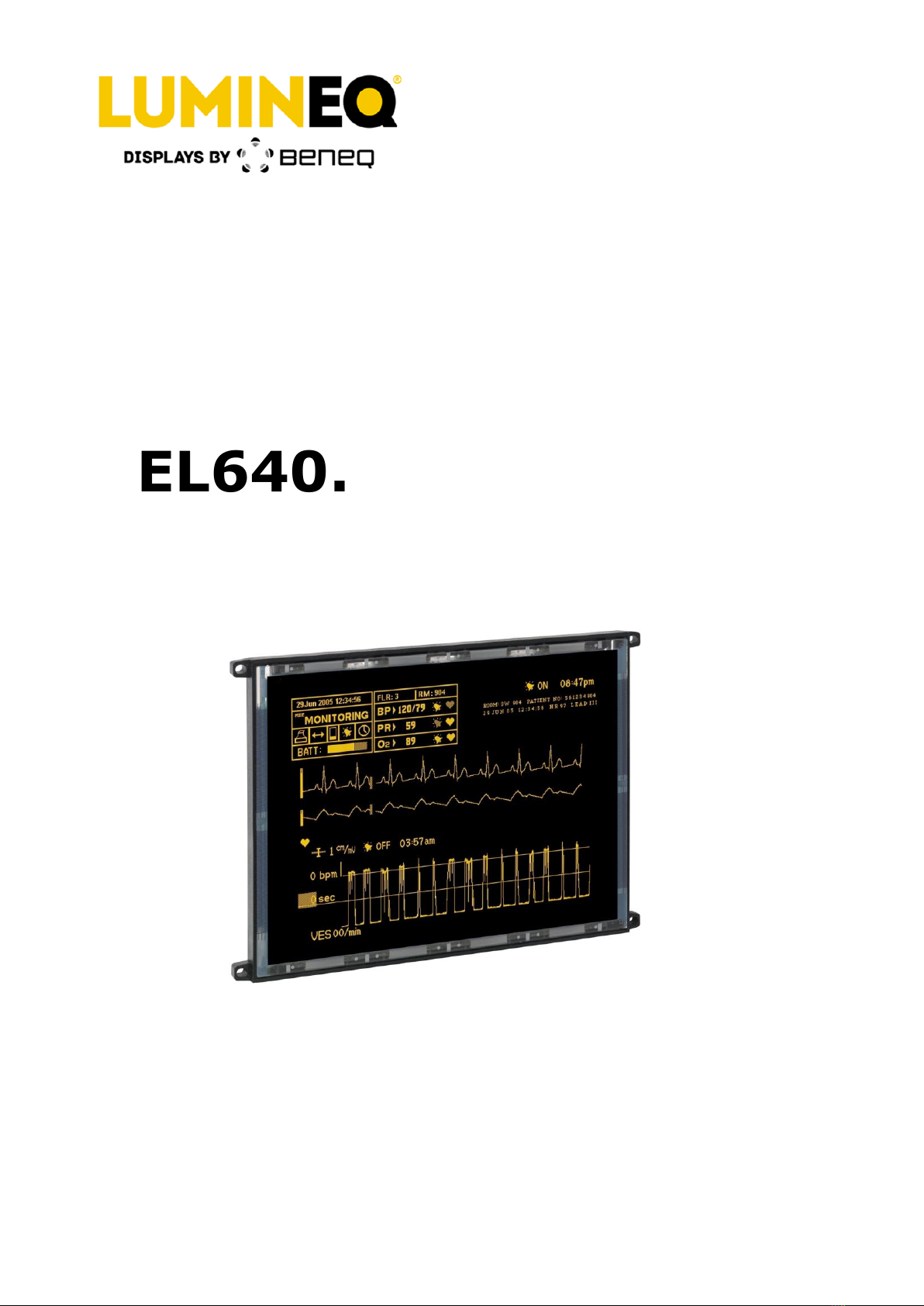
EL640.480-AM LVDS
10.1” Thin Film
Electroluminescent
VGA Flat Panel Display
Operation
Manual
Beneq Oy
Olarinluoma 9
Tel. +358 9 7599 530
VAT ID FI19563372
FI-02200 Espoo
Fax +358 9 7599 5310
www.beneq.com
Finland
lumineq@beneq.com
www.lumineq.com
Date: February 7, 2017
Document number: ED001137 Rev. A
Page | 1
EL640.480-AM LVDS
Operation Manual

Operation Manual
EL640.480-AM LVDS
Beneq Oy
Olarinluoma 9
Tel. +358 9 7599 530
VAT ID FI19563372
FI-02200 Espoo
Fax +358 9 7599 5310
www.beneq.com
Finland
lumineq@beneq.com
www.lumineq.com
Date: February 7, 2017
Document number: ED001137 Rev. A
Page | 2
Table of contents:
1EL640.480-AM LVDS display .................................................................................................................. 3
1.1 Features and benefits .................................................................................................................... 3
1.2 Options ........................................................................................................................................ 3
2Installation and handling....................................................................................................................... 4
2.1 Mounting...................................................................................................................................... 4
2.2 Cleaning....................................................................................................................................... 4
2.3 Cable length ................................................................................................................................. 5
2.4 Avoiding burn-in ........................................................................................................................... 5
3Specifications ...................................................................................................................................... 5
3.1 Control basics ............................................................................................................................... 5
3.2 Power .......................................................................................................................................... 5
3.3 Connectors ................................................................................................................................... 6
3.3.1 Video/power connector........................................................................................................... 6
3.3.2 Dimming connector................................................................................................................ 7
3.4 Interfacing ................................................................................................................................... 7
3.4.1 Data packing......................................................................................................................... 8
3.4.2 Video input data timing diagrams ............................................................................................ 9
3.4.3 Timing chart and specifications.............................................................................................. 10
3.4.4 Dip switch settings............................................................................................................... 12
3.5Self-test..................................................................................................................................... 13
3.6 Optical ....................................................................................................................................... 14
3.7 Dimming .................................................................................................................................... 14
3.8 Reliability ................................................................................................................................... 17
3.9 Safety and EMI ........................................................................................................................... 17
3.10 Environmental ............................................................................................................................ 17
3.11 Mechanical characteristics ............................................................................................................ 18
3.12 Component envelope ................................................................................................................... 19
4Description of warranty....................................................................................................................... 20
5Ordering information .......................................................................................................................... 21
6Support and service............................................................................................................................ 21
7RoHS II............................................................................................................................................. 21

Operation Manual
EL640.480-AM LVDS
Beneq Oy
Olarinluoma 9
Tel. +358 9 7599 530
VAT ID FI19563372
FI-02200 Espoo
Fax +358 9 7599 5310
www.beneq.com
Finland
lumineq@beneq.com
www.lumineq.com
Date: February 7, 2017
Document number: ED001137 Rev. A
Page | 3
1EL640.480-AM LVDS display
This manual describes the Beneq ICEBrite™EL640.480-AM LVDS (Low Voltage Differential
Signaling) display. This 6.4" diagonal VGA resolution display offers exceptional performance
for demanding conditions. Utilizing Beneq’s proprietary ICEBrite (Integrated Contrast
Enhancement) technology, this display excels in ambient light environments ranging from
dark to nearly sunlight-bright. This technology achieves very high contrast and exceptionally
clear images.
The EL640.480-AM LVDS display is capable of instant-on performance from -60 °C to +105
°C with instant pixel response over the entire temperature range, and no motion blur.
Lumineq® TFEL displays, ideal for embedded applications, represent the best viewing
experience available for extreme conditions. TFEL displays are reliable, robust and proven in
use in the harshest places on earth and in space. Excellent vibration and shock resistance,
together with a compact and lightweight build, make these displays better than the rest.
1.1 Features and benefits
Very wide operating temperature from -60 C to +85 C
Operating survival from -60 C to +105 C
Excellent visual performance
Good contrast
Wide viewing angle
Reliable, long operating life
Extremely rugged and durable
Low EMI emissions
Rapid display response
LVDS interface, supports JEIDA and VESA data packing
Locking connector
Analog dimming
1.2 Options
Conformal coating and anti-glare filter options are available for this display.
The conformal coating option adds a protective layer to the display for applications in which
the display may be subjected to high humidity, dust, or salt mist.
The anti-glare filter diffuses light and improved viewing in challenging indoor light conditions.

Operation Manual
EL640.480-AM LVDS
Beneq Oy
Olarinluoma 9
Tel. +358 9 7599 530
VAT ID FI19563372
FI-02200 Espoo
Fax +358 9 7599 5310
www.beneq.com
Finland
lumineq@beneq.com
www.lumineq.com
Date: February 7, 2017
Document number: ED001137 Rev. A
Page | 4
2Installation and handling
The mechanical package consists of the display panel and electronic circuit board adhesively
bonded together and mounted in a plastic bezel. The bezel supplies the mounting ears and
protects otherwise exposed leads. The display is made of glass material and must be handled
with care.
CAUTION: The display uses CMOS and power MOSFET devices. These components are
electrostatic-sensitive. Unpack, assemble, and examine this assembly in a static-controlled
area only. When shipping the display, use packing materials designed for protection of
electrostatic-sensitive components.
Do not drop, bend or flex the display. Do not allow objects to strike the surface of the
display.
2.1 Mounting
The EL640.480-AM LVDS display is designed to facilitate the mounting of optical treatments
and touch screens on the viewing side of the display. To this end, the glass extends in front
of the mounting bezel by approximately 0.5 mm (0.02") It is imperative that any mounting
scheme apply uniform pressure across the glass at all times. Pressure applied only to the
corners or edge of the glass is likely to cause breakage.
Mounting should be done using the mounting ears only. Use either metric M3 screws
tightened to 3.5 Nm maximum, or unified #4 screws tightened to 4.7 in/lb. maximum.
CAUTION: Properly mounted, this display can withstand high shock loads and severe
vibration in aggressive environments. However, the glass panel used in this display will break
when subjected to bending stresses, high impact, or excessive loads.
CAUTION: To prevent injury in the event of a glass breakage, a protective overlay should be
used on the viewer side of the display.
WARNING: These products generate voltages capable of causing personal injury (high
voltage up to 230 VAC). Do not touch the display electronics during operation.
2.2 Cleaning
As with any glass or coated surface, care should be taken to minimize scratching. Clean the
display glass with mild, water-based detergents only. Apply the cleaner sparingly to a soft
cloth, and then wipe the display. Disposable cleaning cloths are recommended to minimize
the risk of inadvertently scratching the display with particles embedded in a re-used cloth.
The TAB (tape-automated bonding) leads between the electronics and the display glass are
very sensitive to handling. When cleaning the edges of the display glass, special care should
be taken not to damage the leads.

Operation Manual
EL640.480-AM LVDS
Beneq Oy
Olarinluoma 9
Tel. +358 9 7599 530
VAT ID FI19563372
FI-02200 Espoo
Fax +358 9 7599 5310
www.beneq.com
Finland
lumineq@beneq.com
www.lumineq.com
Date: February 7, 2017
Document number: ED001137 Rev. A
Page | 5
2.3 Cable length
Do not exceed the maximum cable length of 600 mm (24 in.). Longer cables may cause data
transfer problems between the data transmitted and the display input connector. Excessive
cable lengths can pick up unwanted EMI.
2.4 Avoiding burn-in
As with other light-emitting displays, displaying fixed patterns on the screen can causes
burn-in where luminance variations can be noticed. Use a screensaver or image inversion to
avoid causing burn-in on the display.
3Specifications
3.1 Control basics
The TFEL panel is a matrix structure with column and row electrodes arranged in an X-Y
formation. Light is emitted when an AC voltage of sufficient amplitude is applied at a row-
column intersection. The display operation is based on the differential signaling, line-at-a-
time data addressing scheme. Required operating voltages are provided by an integrated
DC/DC converter.
Unless otherwise specified, the TFEL panel performance characteristics are guaranteed when
measured at 25 °C.
3.2 Power
Please refer to Table 1. All internal high voltages are generated from the display supply
voltage (VH). The Supply voltage (VH) should be present whenever video input signals are
applied. The minimum and maximum specifications in this manual should be met, without
exception, to ensure the long-term reliability of the display. Beneq does not recommend
operation of the display outside these specifications.
Table 1. Input power requirement
Description
Symbol
Min
Typ.
Max
Units
Notes
Supply voltage
VH
10.8
12.0
13.2
V
Absolute max 15 VDC
Supply current
IL
-
0.9
2.0
A
VH= 12 VDC
Power consumption
PH
-
11
24
W
VH = 12 VDC
CAUTION: Absolute maximum ratings are those values beyond which damage to the device
may occur. There is no overcurrent protection on VH input to protect against catastrophic
faults. Beneq recommends the use of a series fuse on the 12 volt supply. A general guideline
is to rate the fuse at 1.8 to 2 times the display maximum current rating
Operation Manual
EL640.480-AM LVDS
Beneq Oy
Olarinluoma 9
Tel. +358 9 7599 530
VAT ID FI19563372
FI-02200 Espoo
Fax +358 9 7599 5310
www.beneq.com
Finland
lumineq@beneq.com
www.lumineq.com
Date: February 7, 2017
Document number: ED001137 Rev. A
Page | 6
Table 2. Video input requirements
Description
Symbol
Min
Max
Units
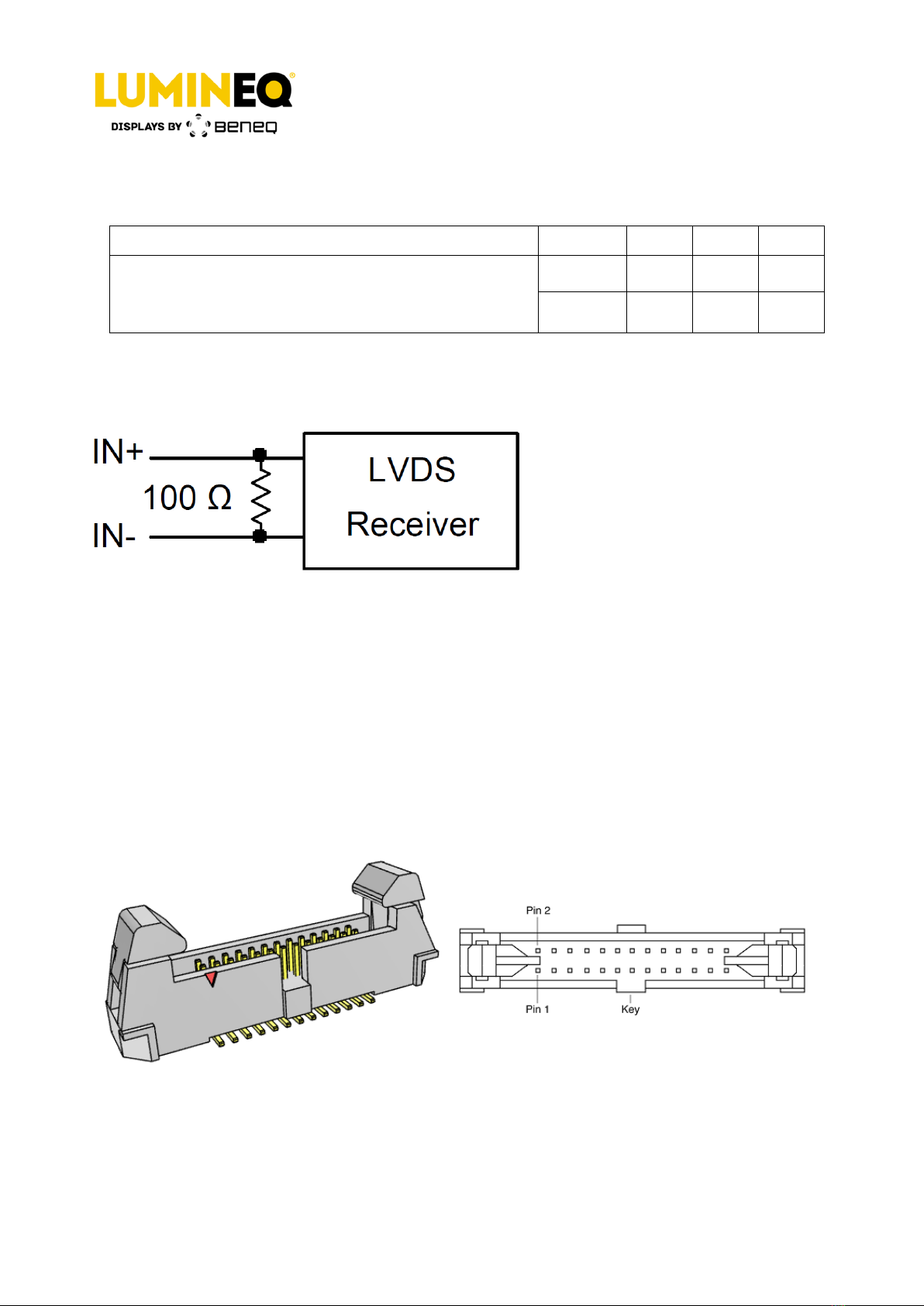
Differential input voltage for LVD receiver threshold
VIH
-
+100
mV
VIL
-100
-
mV
Notes: VCM=+1.2 V
VCM is common mode voltage of LVDS transmitter/receiver
The input terminal of LVDS receiver is terminated with 100 Ω series resistors
Figure 1. LVDS Input
3.3 Connectors
3.3.1 Video/power connector
The video/power connector is J3: a 26-pin, 1.27 mm pitch connector (Picture 1).The display
uses the Samtec EHF-113-01-L-D-SM or equivalent locking connector matching the pinouts in
Table 3. The mating connector is in the Samtec TCSD family of cable strips. The proper
connector, user-specified cable length, and connector configuration are supplied as a single
unit from Samtec. Consult your Samtec representative for the cable/connector options.
Compatibility with non-Samtec equivalents should be verified before use.
Figure 2. Samtec EHF-113-01-L-D-SM connector

Operation Manual
EL640.480-AM LVDS
Beneq Oy
Olarinluoma 9
Tel. +358 9 7599 530
VAT ID FI19563372
FI-02200 Espoo
Fax +358 9 7599 5310
www.beneq.com
Finland
lumineq@beneq.com
www.lumineq.com
Date: February 7, 2017
Document number: ED001137 Rev. A
Page | 7
Table 3. Display J3 connector pinout
Pin
Signal
Description
Pin
Signal
Description
1
NC
Not Connected
2
NC
Not Connected
3
NC
Not connected
4
NC
Not connected
5
GND
Ground
6
NC
Not connected
7
IN3-
LVDSBUS.IN3-
8
IN3+
LVDSBUS.IN3+
9
GND
Ground
10
CLK-
LVDSBUS.CLK_IN-
11
CLK+
LVDSBUS.CLK_IN+
12
GND
Ground
13
IN2-
LVDSBUS.IN2-
14
IN2+
LVDSBUS.IN2+
15
GND
Ground
16
IN1-
LVDSBUS.IN1-
17
IN1+
LVDSBUS.IN1+
18
GND
Ground
19
IN0-
LVDSBUS.IN0-
20
IN0+
LVDSBUS.IN0+
21
GND
Ground
22
Vin
+12 VDC power
23
GND
Ground
24
Vin
+12 VDC power
25
GND
Ground
26
Vin
+12 VDC power
3.3.2 Dimming connector
The dimming connector is a JST part number B2B-PH-K-S(LF)(SN), which is a 2-pin, 2 mm
header. The recommended mate is a JST part number PHR-2 (housing) with JST part number
SPH-004T-P0.5S (crimp for 28-34 AWG wire).
Refer to the dimming section below, under optical performance.
3.4 Interfacing
LVDS interface provides a low-cost, high noise immunity method for controlling the TFEL
display. Many off-the-shelf chipsets are available for interfacing to flat panel displays through
LVDS. If your application does not require chip-level integration, there are many vendors that
can supply board-level solutions. The EL640.40-AM LVDS display support the following LVDS
data packings:
LVDS single bus, 18 bpp, VESA data packing
LVDS single bus, 18 bpp, JEIDA data packing
LVDS single bus, 24 bpp, VESA data packing
LVDS single bus, 24 bpp, JEIDA data packing
Operation Manual
EL640.480-AM LVDS
Beneq Oy
Olarinluoma 9
Tel. +358 9 7599 530
VAT ID FI19563372
FI-02200 Espoo
Fax +358 9 7599 5310
www.beneq.com
Finland
lumineq@beneq.com
www.lumineq.com
Date: February 7, 2017
Document number: ED001137 Rev. A
Page | 8
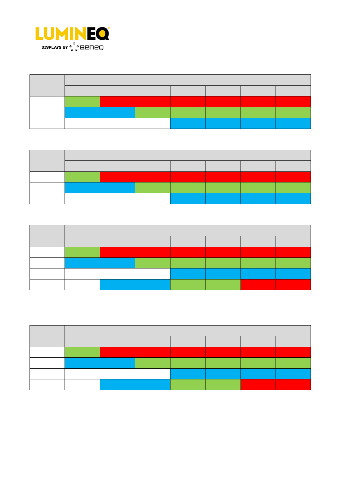
3.4.1 Data packing
Channel
Bit position
6
5
4
3
2
1
0
IN0
bit 0
bit 5
bit 4
bit 3
bit 2
bit 1
bit 0
IN1
bit 1
bit 0
bit 5
bit 4
bit 3
bit 2
bit 1
IN2
DE
Vsync
Hsync
bit 5
bit 4
bit 3
bit 2
Table 4. LVDS single bus, 18 bpp, VESA data packing.
Channel
Bit position
6
5
4
3
2
1
0
IN0
bit 2
bit 7
bit 6
bit 5
bit 4
bit 3
bit 2
IN1
bit 3
bit 2
bit 7
bit 6
bit 5
bit 4
bit 3
IN2
DE
Vsync
Hsync
bit 7
bit 6
bit 5
bit 4
Table 5. LVDS single bus, 18 bpp, JEIDA data packing.
Channel
Bit position
6
5
4
3
2
1
0
IN0
bit 0
bit 5
bit 4
bit 3
bit 2
bit 1
bit 0
IN1
bit 1
bit 0
bit 5
bit 4
bit 3
bit 2
bit 1
IN2
DE
Vsync
Hsync
bit 5
bit 4
bit 3
bit 2
IN3
NIU
bit 7
bit 6
bit 7
bit 6
bit 7
Bit 6
Note: NIU = Not In Use
Table 6. LVDS single bus, 24 bpp, VESA data packing.
Channel
Bit position
6
5
4
3
2
1
0
IN0
bit 2
bit 7
bit 6
bit 5
bit 4
bit 3
bit 2
IN1
bit 3
bit 2
bit 7
bit 6
bit 5
bit 4
bit 3
IN2
DE
Vsync
Hsync
bit 7
bit 6
bit 5
bit 4
IN3
NIU
bit 1
bit 0
bit 1
bit 0
bit 1
Bit 0
Note: NIU = Not In Use
Table 7. LVDS single bus, 24 bpp, JEIDA data packing.
Operation Manual
EL640.480-AM LVDS
Beneq Oy
Olarinluoma 9
Tel. +358 9 7599 530
VAT ID FI19563372
FI-02200 Espoo
Fax +358 9 7599 5310
www.beneq.com
Finland
lumineq@beneq.com
www.lumineq.com
Date: February 7, 2017
Document number: ED001137 Rev. A
Page | 9
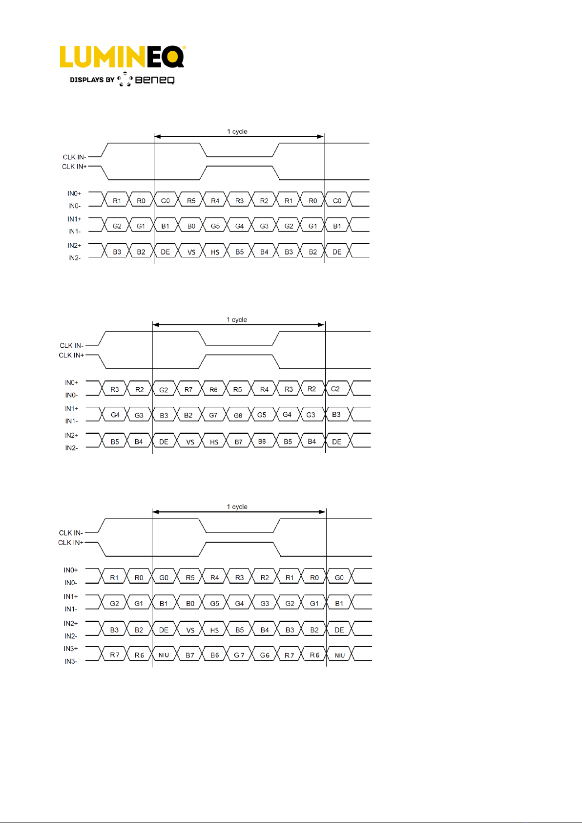
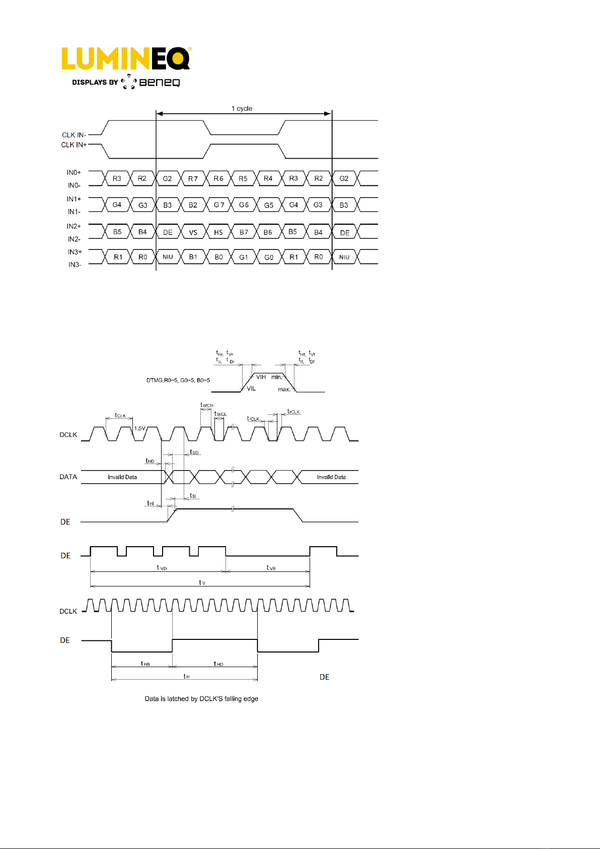
3.4.2 Video input data timing diagrams
Figure 3. Video input data timing diagram, 18 bpp, VESA data packing
Figure 4. Video input data timing diagram, 18 bpp, JEIDA data packing
Figure 5. Video input data timing diagram, 24 bpp, VESA data packing
Operation Manual
EL640.480-AM LVDS
Beneq Oy
Olarinluoma 9
Tel. +358 9 7599 530
VAT ID FI19563372
FI-02200 Espoo
Fax +358 9 7599 5310
www.beneq.com
Finland
lumineq@beneq.com
www.lumineq.com
Date: February 7, 2017
Document number: ED001137 Rev. A
Page | 10
Figure 6. Video input data timing diagram, 24 bpp, JEIDA data packing
3.4.3 Timing chart and specifications
Figure 7. Timing chart

Operation Manual
EL640.480-AM LVDS
Beneq Oy
Olarinluoma 9
Tel. +358 9 7599 530
VAT ID FI19563372
FI-02200 Espoo
Fax +358 9 7599 5310
www.beneq.com
Finland
lumineq@beneq.com
www.lumineq.com
Date: February 7, 2017
Document number: ED001137 Rev. A
Page | 11
Table 8. Timing specifications
Description
Symbol
Min.
Typ.
Max.
Unit
DCLK
Cycle frequency
1/tCLK
22.29
25.2
34.2
MHz
Low level width
tWCL
10
-
-
ns
High level width
tWCH
10
-
-
Rise/Fall time
trCLK, tfCLK
-
-
12
Duty
D
0.4
0.5
0.6
-
DE
Set-up time
tSI
8
-
-
ns
Hold time
tHI
8
-
-
Rise/Fall time
tIr, tIf
-
-
12
ns
Horizontal cycle
tH
750
800
1000
ns
Horizontal valid data width
tHD
640
640
640
tCLK
Horizontal porch width
tHB
110
160
360
Vertical cycle
tV
495
525
570
Vertical data width
tVD
480
480
480
tH
Vertical porch width
tVB
15
45
110
DATA
Set-up time
tSD
8
-
-
Hold time
tHD
8
-
-
ns
Rise/fall time
tDr, tDf
-
-
12
ns
Figure 8. LVDS receiver timing chart.
Operation Manual
EL640.480-AM LVDS
Beneq Oy
Olarinluoma 9
Tel. +358 9 7599 530
VAT ID FI19563372
FI-02200 Espoo
Fax +358 9 7599 5310
www.beneq.com
Finland
lumineq@beneq.com
www.lumineq.com
Date: February 7, 2017
Document number: ED001137 Rev. A
Page | 12
Table 9. LVDS receiver timing
Description
Symbol
Min.
Typ.
Max
Unit
DCLK
Frequency
1/tCLK
22.29
25.2
34.2
MHz
RinX
(X=0,1,2)
0 data position
tRPO
1/7*tCLK-0.49
1/7*tCLK
1/7*tCLK+0.49
ns
1st data position
tRP1
-0.49
0
+0.49
2nd data postion
tRP2
6/7*tCLK-0.49
6/7*tCLK
6/7*tCLK+0.49
3rd data position
tRP3
5/7*tCLK-0.49
5/7*tCLK
5/7*tCLK+0.49
4th data position
tRP4
4/7*tCLK-0.49
4/7*tCLK
4/7*tCLK+0.49
5th data position
tRP5
3/7*tCLK-0.49
3/7*tCLK
3/7*tCLK+0.49
6th data position
tRP6
2/7*tCLK-0.49
2/7*tCLK
2/7*tCLK+0.49
3.4.4 Dip switch settings
Figure 9. Dip switch
Table 10. Dip switch settings
Dip
OFF
ON
1
4 levels of grayscales
5 levels of grayscales
2
VESA Standard
JEIDA Standard
3
Red scale 0
See color settings table
4
Red scale 1
See color settings table
5
Green scale 0
See color settings table
6
Green scale 1
See color settings table
7
Blue scale 0
See color settings table
8
Blue scale 1
See color settings table
9
Normal operation
Self-test 1
10
Normal operation
Self-test 2
Default: All OFF

Operation Manual
EL640.480-AM LVDS
Beneq Oy
Olarinluoma 9
Tel. +358 9 7599 530
VAT ID FI19563372
FI-02200 Espoo
Fax +358 9 7599 5310
www.beneq.com
Finland
lumineq@beneq.com
www.lumineq.com
Date: February 7, 2017
Document number: ED001137 Rev. A
Page | 13
Table 11. Color settings
3.5 Self-test
The display incorporates two self-test modes. The self-test mode is selected by the dip
switch. See figure 6, dip switch and table 9, dip switch settings.
Red
Red scale 0 off –Red scale 1 off (default)
Red value 1/1
Red scale 0 on –Red scale 1 off
Red value 1/2
Red scale 0 off –Red scale 1 on
Red value 1/4
Red scale 0 on –Red scale 1 on
Red value 1/8
Green
Green scale 0 off –Green scale 1 off (default)
Green value 1/1
Green scale 0 on –Green scale 1 off
Green value 1/2
Green scale 0 off –Green scale 1 on
Green value 1/4
Green scale 0 on –Green scale 1 on
Green value 1/8
Blue
Blue scale 0 off –Blue scale 1 off (default)
Blue value 1/1
Blue scale 0 on –Blue scale 1 off
Blue value 1/2
Blue scale 0 off –Blue scale 1 on
Blue value 1/4
Blue scale 0 on –Blue scale1 on
Blue value 1/8
Operation Manual
EL640.480-AM LVDS
Beneq Oy
Olarinluoma 9
Tel. +358 9 7599 530
VAT ID FI19563372
FI-02200 Espoo
Fax +358 9 7599 5310
www.beneq.com
Finland
lumineq@beneq.com
www.lumineq.com
Date: February 7, 2017
Document number: ED001137 Rev. A
Page | 14
3.6 Optical
Table 12. Optical characteristics
Luminance
Lon (areal), min
40.0 cd/m²
Screen center
Lon (areal), typ
55.0 cd/m²
Screen center
Loff (areal), max
0.2 cd/m²
Center and four corners
Non-uniformity
All pixels fully lit
35 %
Maximum difference two of five points, using the
formula: LNU %=[1- (min_lum/max_lum)] x
100 %
Luminance variation (temperature)
Maximum
15 %
Across operating temperature range
Luminance variation (time)
Maximum
20 %
10,000 hours at 25 °C ambient
Viewing angle
Minimum
179°
Contrast ratio
Typical
40:1
@ 500 lux ambient
3.7 Dimming
This display includes an internal frame buffer. The display internal 132 Hz frame rate and the
display brightness are independent of user-supplied input data timing.
Analog dimming control circuitry is present on this display model. This feature allows manual
analog dimming of the brightness from 100 % to approximately 5 % (dark) of the full
brightness.

Operation Manual
EL640.480-AM LVDS
Beneq Oy
Olarinluoma 9
Tel. +358 9 7599 530
VAT ID FI19563372
FI-02200 Espoo
Fax +358 9 7599 5310
www.beneq.com
Finland
lumineq@beneq.com
www.lumineq.com
Date: February 7, 2017
Document number: ED001137 Rev. A
Page | 15
The J2 analog dimming connector is a JST 2-pin connector, part number B2B-PH-K-
S(LF)(SN).
Figure 10. Dimming connector J2
To utilize analog dimming, connect one end of a 50 kΩexternal potentiometer to pin 2 of
connector J2 and connect the wiper of the potentiometer to pin 1. With 50 kΩacross the
dimming connector, the display brightness will be at maximum. Decreasing the resistance will
decrease the display brightness immediately. Alternatively, an external voltage or current
mode D/A converter may be used to facilitate dimming by sinking a maximum of 100 µA (for
maximum dimming) from pin 1 to pin 2 of the dimming connector.
See the figures 7 and 8 for typical analog dimming performance.

Operation Manual
EL640.480-AM LVDS
Beneq Oy
Olarinluoma 9
Tel. +358 9 7599 530
VAT ID FI19563372
FI-02200 Espoo
Fax +358 9 7599 5310
www.beneq.com
Finland
lumineq@beneq.com
www.lumineq.com
Date: February 7, 2017
Document number: ED001137 Rev. A
Page | 16
Figure 11. Analog dimming adjustment
Figure 12. External voltage dimming

Operation Manual
EL640.480-AM LVDS
Beneq Oy
Olarinluoma 9
Tel. +358 9 7599 530
VAT ID FI19563372
FI-02200 Espoo
Fax +358 9 7599 5310
www.beneq.com
Finland
lumineq@beneq.com
www.lumineq.com
Date: February 7, 2017
Document number: ED001137 Rev. A
Page | 17
3.8 Reliability
The MTBF (mean time between failures) is a minimum of 50,000 hours at 25 °C ambient,
except for performance characteristics with an otherwise specified life expectancy.
3.9 Safety and EMI
The display will not inhibit the end product from obtaining these certifications:
Safety UL 60601-1, IEC 60950-1
EMI FCC Part 15/J, Class B, EN55022 Level B
3.10 Environmental
Table 13. Environmental characteristics
Temperature
Operating
-60 °C to +85 °C
Operating survival
-60 °C to +105 °C
Non-operating
-60 °C to +110 °C
Humidity
Non-condensing
93 % RH max, @ 40 °C
per IEC 60068-2-78.
Altitude
Operating
0 to 18 km (58k ft.)
per IEC 60068-2-13.
Damp heat
Non-operating
25-55 °C, 95 % RH
Per IEC 60068-2-30.
Vibration
Random
0.05 g²/Hz
ASD level, 5-500 Hz per
IEC 60068-2-64, test Fh.
Shock
Half sine wave
100 g, 4 ms
18 (3 each, 6 surfaces) per
IEC 60068-2-27, test Ea.

Operation Manual
EL640.480-AM LVDS
Beneq Oy
Olarinluoma 9
Tel. +358 9 7599 530
VAT ID FI19563372
FI-02200 Espoo
Fax +358 9 7599 5310
www.beneq.com
Finland
lumineq@beneq.com
www.lumineq.com
Date: February 7, 2017
Document number: ED001137 Rev. A
Page | 18
3.11 Mechanical characteristics
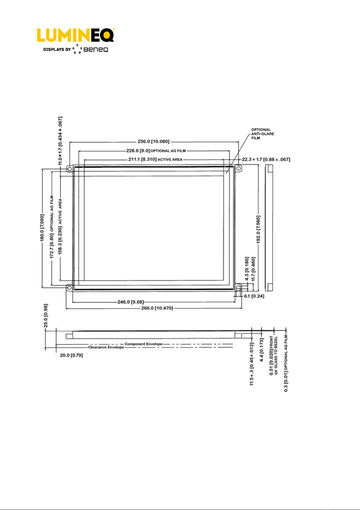
Table 14. Weight and dimensions
Description
Value
Unit
Weight
525 ± 10
g
Display size
266 x 192 (W x H)
Display depth
19 ± 1
mm
Active area
211.1 x 158.3 (W x H)
Fill factor
57 %
Pixel pitch
0.33 x 0.33 (W x H)
mm
Pixel size
0.25 x 0.25 (W x H)
mm
Operation Manual
EL640.480-AM LVDS
Beneq Oy
Olarinluoma 9
Tel. +358 9 7599 530
VAT ID FI19563372
FI-02200 Espoo
Fax +358 9 7599 5310
www.beneq.com
Finland
lumineq@beneq.com
www.lumineq.com
Date: February 7, 2017
Document number: ED001137 Rev. A
Page | 19
3.12 Component envelope
Figure 5 illustrates the distance the components extend behind the display. Tall components
do not necessarily fill this area. Beneq reserves the right to relocate components within the
constraints of the component’s envelope without prior customer notification. For this reason,
Beneq advises users to design enclosure components to be outside the component envelope.
Dimensions are in millimeters; inches in brackets.
Tolerances unless otherwise stated ±0.2 mm
Figure 13. EL640.480-AM LVDS dimensions

Operation Manual
EL640.480-AM LVDS
Beneq Oy
Olarinluoma 9
Tel. +358 9 7599 530
VAT ID FI19563372
FI-02200 Espoo
Fax +358 9 7599 5310
www.beneq.com
Finland
lumineq@beneq.com
www.lumineq.com
Date: February 7, 2017
Document number: ED001137 Rev. A
Page | 20
4Description of warranty
Seller warrants that the Goods will conform to published specifications and be free from
defects in material during warranty time from delivery. To the extent that goods incorporate
third-party-owned software, seller shall pass on seller's licensor's warranty to buyer subject
to the terms and conditions of seller's license.
Warranty repairs shall be warranted for the remainder of the original warranty period. Buyer
shall report defect claims in writing to seller immediately upon discovery, and in any event,
within the warranty period. Buyer must return goods to seller within 30 days of seller’s
receipt of a warranty claim notice and only after receiving seller’s return goods authorization.
Seller shall, at its sole option, repair or replace the goods.
If goods were repaired, altered or modified by persons other than seller, this warranty is
void. Conditions resulting from normal wear and tear and buyer's failure to properly store,
install, operate, handle or maintain the goods are not within this warranty. Repair or
replacement of goods is seller’s sole obligation and buyer's exclusive remedy for all claims of
defects. If that remedy is adjudicated insufficient, Seller shall refund buyer's paid price for
the goods and have no other liability to buyer.
All warranty repairs must be performed at seller’s authorized service center using parts
approved by seller. Buyer shall pay costs of sending goods to seller on a warranty claim and
seller shall pay costs of returning goods to buyer. The turnaround time on repairs will usually
be 30 working days or less. Seller accepts no added liability for additional days for repair or
replacement.
If seller offers technical support relating to the goods, such support shall neither modify the
warranty nor create an obligation of seller. Buyer is not relying on seller’s skill or judgment to
select goods for buyer’s purposes. Seller’s software, if included with goods, is sold as is, and
this warranty is inapplicable to such software.
SELLER DISCLAIMS ALL OTHER WARRANTIES, EXPRESS OR IMPLIED, INCLUDING BUT NOT
LIMITED TO, IMPLIED WARRANTIES OF MERCHANTABILITY AND FITNESS FOR A PARTICULAR
PURPOSE.
Table of contents
Popular Industrial Monitor manuals by other brands

Enovation Controls
Enovation Controls MURPHY HelmView HV780 installation manual

Austin Hughes
Austin Hughes CyberView RP-920 user manual

Hope Industrial Systems
Hope Industrial Systems HIS-UM17-*A Series user manual

FIAMA
FIAMA F8P User manual and maintenance

Jinyoung Contech
Jinyoung Contech VX1500 user manual

Contec
Contec FPD-M21VT-AC user manual


