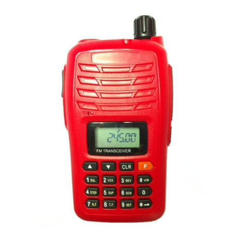
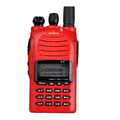
Benison V7 User manual

V7
1
V7
FM TRANSCEIVERS
Service Manual

V7
2
SPECIFICATIONS
GENERAL
Frequency Range 245.0000~245.9875
Working Temperate -10℃~+55℃
Power Supply Requirement DC 7.2V
Current Consumption ≤1.6A(transmit 4W)
Sensitivity Adjust 2~20mV
Antenna impedance 50Ω
TRANSMITTER
Frequency Stability ±5ppm
Output Power 5W(High),1W(Low)
Max Frequency Deviation ≤±2.5KHz
Intermodulation Response Rejection 70dB
Audio Distortion ≤10%
Adjacent Channel Power ≤-65dB
Occupied Bandwidth ≤16KHz
RECEIVER
RF Sensitivity : ≤0.2μV
Audio Frequency Response 300-3000Hz
Audio Output ≥0.5w
Audio Distortion ≤10%
All stated specifications are subject to change without notice or obligation.

V7
3
CIRCUIT DESCRIPTION
1. Frequency configuration
The receiver utilizes double conversion. The first IF is 38.85MHz and the second IF is
450kHz. The first local oscillator signal is supplied from the PLL circuit. The PLL circuit in
the transmitter generates the ecessary frequencies. Fig. 1 shows the frequencies.
2. Receiver
The freauency configuration of the receiver is shown in Fig.2.
1) Front - end RF amplifier
An incoming signal from the antenna is applied to an RF amplifier (T201) after passing
through a transmit/receive switch circuit (D101 ,D102,D103) and a 3-pole LC
filter(L203,L204).After the signal is amplified (T201), the signal is filtered by a band pass
filter (a 3-pole LC filter) (L217,L218,L221) to eliminate unwanted signals before it is
passed to the first mixer. The voltage of these diodes are controlled by to track the
MPU(U811) center frequency of the band pass filter. (See Fig. 2)

V7
4
2) First Mixer
The signal from the RF amplifier is heterodyned with the first local oscillator signal from
the PLL frequency synthesizer circuit at the first mixer (T202) to create a 38.85MHz first
intermediate frequency (1st IF) signal. The first IF signal is then fed through crystal filters
(FL231,FL232) to further remove spurious signals.
3) IF amplifier
The first IF signal is amplified by T203, and then enters U200 (FM processing IC). The
signal is heterodyned again with a second local oscillator signal within U200 to create a
450kHz second IF signal. The second IF signal is then fed through a 450kHz ceramic filter
(FL240) to further eliminate unwanted signals before it is amplified and FM detected in
FL240.
4) AF amplifier
The recovered AF signal obtained from U200 goes to the microprocessor(U811). The
processed AF signal passes through an AF volume control and is amplified to a sufficient
level to drive a loud speaker by an AF power amplifier (U481).
5) Squelch
Part of the AF signal from the IC enters the FM IC again,and the noise component is
amplified and rectified by a filter and an amplifier to produce a DC voltage corresponding
to the noise level. The DC signal from the FM IC goes to the analog port of the
microprocessor (U811). U811 determines whether to output sounds from the speaker by
checking whether the input voltage is higher or lower than the preset value.To output
sounds from the speaker, U811 sends a high signal to the AF Power Iines and turns U481
on through T471,T472.
6) Receive signaling
QT/DQT
The output signal from FM IC (U200) enters the microprocessor(U811) .U811 determines
whether the QT or DQT matches the preset value, and controls the AF Power and the
speaker output sounds according to the squelch results
3. PLL frequency synthesizer
The PLL circuit generates the first local oscillator signal for reception and the RF signal for
transmission.
1) PLL
The frequency step of the PLL circuit is 5 and 6.25kHz and so on. A 16.8MHz reference
oscillator signal is divided at U301 by a fixed counter to produce the 5 or 6.25kHz
reference frequency. The voltage controlled oscillator (VCO) output signal is buffer
amplified by T373, then divided in U301 by a programmable counter . The divided signal is
compared in phase with the 5 or 6.25kHz reference signal in the phase comparator in
U301. The output signal from the phase comparator is filtrered through a low-pass filter
and passed to the VCO to control the oscillator frequency.
2) VCO
The operating frequency is generated by T331 in transmit mode and T357 in receive
mode. The oscillator frequency is controlled by applying the VCO control voltage, obtained
from the phase comparator, to the varactor diodes (D331 and D332 in transmit mode and
D350 and D351 in receive mode). The TC/RC pin is set low in receive mode causing T192
off, and turn T291 on . The TC/RC pin is set hight in transmit mode causing T291 off,and
T192,T191 on.

V7
5
3) UNLOCK DETECTOR
If a pulse signal appears at the LD pin of U301, an unlock condition occurs, and the DC
voltage obtained from D309, and C306 causes the voltage applied to the PLL-LD pin of
the microprocessor to go low. When the microprocessor detects this condition, the
transmitter is disabled, ignoring the push-totalk switch input signal. ( See Fig.3)
4. Transmitter
1)Microphone Amplifier
The signal from the microphone passes through U411.When encoding DTMF,it is turned
OFF for muting the microphone input signal by T414.The signal passes through the Audio
processor(U411) for the maximum deviation adjustment,and goes to the VCO modulation
input.
2)Drive and Final Amplifier
The signal from the T/R switch(D100) is amplified by the pre-drive(T101.T102) and drive
amplifier(T105) to 50mW.The output of the drive amplifier is amplified by the RF power
amplifier(T107) to 4.0W(1W when the power is low).the RF power amplifier consists of two
MOS FET stages.The output of the RF power amplifier consists of two MOS FET stages.
The output of the RF power amplifier is then passed through the harmonic filter (LPF) and
antenna switch (D101,D102)and applied to the antenna terminal.
5. Power supply
There are four 5V power supplies for the microprocessor: 5M,5C,5R,and 5T,5M for
microprocessor is always output while the power is on.5M for microprocessor is always
output while the power is on.5M is always output,but turns off when the power is turned off
to prevent malfunction of the microprocessor.
5C is a common 5V and is output when SAVE is not set to OFF.
5R is 5V for reception and output during reception.
5T is 5V for transmission and output during transmission.
6.Control Circuit
The control circuit consists of a microprocessor (U811) and its peripheral circuits.it
controls the TX-RX unit.U811 mainly performs the following:
(1) Switching between transmission and reception by the PTT signal input.
(2) Reading system,group,frequency,and program data from the memory circuit.
(3) Sending frequency program data to the PLL.
(4) Controlling squelch on/off by the DC voltage from the squelch circuit.
(5) Controlling the audio mute circuit by the decode data input.
(6) Transmitting tone and encode data.

V7
6
1)Memory Circuit
Memory circuit consists of the CPU (U811) and an EEPROM(U821).An EEPROM has a
capacity of 32k bits that contains the transceiver control program for the CPU and data
such as Transceiver channels and operation features
2)Low Battery Warning
The battery voltage is checked using by the microprocessor.
(1) The red LED blinks when the battery voltage falls below 6.2V.
(2) A Warning tone generates when the red LED blinking. ( See Fig.4)

V7
7
ADJUSTMENT
Required Test Equipment
The following items are required to adjust radio parameters:
1. Regulated power supply
Supply voltage: 5-14V DC
Current: 3A or more
2. Digital multimeter
Voltage range: FS = Approx. 20V
Current: 10A or more
Input resistance: High impedance
3. Oscilloscope
Measurable frequency: Audio frequency
4. Audio dummy load
Impedance: 8 ohm
Dissipation: 1W or more
Jack: 3.5mm
5. SSG
Output frequency: 200MHz or more
Output level: -20dBu/0.1uV -120dBu/1V
Modulation: FM
6. Spectrum Analyzer
Measuring range: Up to 2GHz or more
7. Power meter
Measurable frequency: Up to 200MHz
Impedance: 50, unbalanced
Measuring range: 0.1W -10W
8. Audio volmeter
Measurable frequency: Up to 100kHz
Sensitivity: 1mV to 10V
9. Audio generator
Output frequency: 67Hz to 10kHz

V7
8
Output impedance: 600, unbalanced
10.Distortion meter/SINAD meter
Measurable frequency: 1kHz
Input level: Up to 40dB
Distortion: 1% - 100%
11.Frequency counter
Measurable frequency: Up to 200MHz
Measurable stability: Approx. +/-0.1ppm
12.Linear detector
Measurable frequency: Up to 200MHz
Characteristics: Flat
CN: 60dB or more
Note
Standard modulation: 1kHz +/-2.5kHz/DEV
Reference sensitivity: 12dB SINAD
Specified audio output leve: 200mW at 8

Comment Footprint Quantity
C255 C170 C424 C482 C811 C812
C402 C331 C241 C492
C256 C181 C412 C417 C423 C444
C474 C476 C546 C548 C549 C494
C193 C817 C818 C306 C257 C115
C131 C231 C236 C243 C253 C261
C262 C302 C307 C491 C493 C821
C840 C843 C844 C824 C108
C164 C180 C291 C292 C392 C451
C472 C473 C475 C547 C827 C820
C191 C361 C128 C223 C226 C232
C235 C248 C251 C252 C344 C822
C841 C845 C903 C908 C910 C336
N.U 0402 1 C165
C167 C168 C294 C391 C435 C446
C293 C192 C194 C114 C362 C363
C107 C112 C125 C129 C132 C143
C210 C211 C214 C227 C247 C106
C102 C215 C109 C207 C213 C222
C303
C173 C177 C401 C419 C421 C337
C371 C831 C305 C376 C378 C113
C119 C123 C343 C345 C350 C324
C849 C902
472P 0402 3 C413 C481 C282
273P 0402 1 C418
223P 0402 5 C420 C422 C515 C521 C523
473P 0402 4 C441 C445 C483 C281
332P 0402 3 C442 C448 C846
680P 0402 2 C443 C848
820P 0402 1 C447
221P 0402 3 C484 C485 C284
C836 C837 C838 C839 C832 C833
C834 C835 C204 C206 C218 C234
C316 C280 C155
7P 0402 2 C229 C372
N.C 0402 2 C127 C116
C355 C340 C111 C202 C216 C219
C224 C246 C317 C200 C153 C150
C147 C304
5P 0402 1 C338
2P 0402 2 C339 C205
9
EIA 0402 Chip capacitors
Designators
14040210P
0402103P
31
200402102P
150402NC
0402470P
100402100P
350402104P
30

Comment Footprint Quantity
0.5P 0402 2 C341 C356
39P 0402 1 C351
15P 0402 3 C373 C225 C142
22P 0402 6 C377 C332 C825 C826 C104 C100
6.8nH 0402 1 C118
1P 0402 3 C220 C217 C334
8P 0402 2 C221 C354
18P 0402 2 C233 C242
220P 0402 2 C244 C245
27P 0402 1 C254
101P 0402 4 C308 C309 C310 C311
392P 0402 1 C842
105P 0402 1 C847
470p 0402 1 C909
4P 0402 1 C353
Comment Footprint Quantity
NC 0603 4 C130 C126 C134 C137
5P 0603 3 C154 C151 C149
1P 0603 1 C148
470P 0603 1 C145
102P 0603 1 C138
15P 0603 1 C136
10P 0603 1 C135
33P 0603 1 C133
Comment Footprint Quantity
E405 E423 E514 E337 E301 E281
E302
105P 0805 2 C471 C901
6.8uF 0805 1 E173
2.2uF 0805 1 E417
223P 0805 1 E452
E471 E482 E362 E232 E248 E908
E910
0.1uF 0805 2 E319 E321
1uF 0805 2 E320 E126
Comment Footprint Quantity
22uF EIA3528 1 E324
100uF EIA6032 1 E483
Designators
Polarized capacitors
Designators
7080510uF
EIA 0603 Chip capacitors
Designators
EIA 0805 Chip capacitors
EIA 0402 Chip capacitors
Designators
708054.7uF
10

Comment Footprint Quantity
1K5 0402 3 R255 R422 R104
10R 0402 4 R249 R450 R484 R111
2K2 0402 5 R405 R472 R322 R300 R847
R826 R825 R301 R171 R179 R444
R449 R471 R476 R481 R518 R520
R545 R827 R415 R304 R372 R841
R848 R101 R292
150K(F) 0402 5 R165 R166 R168 R169 R170
150k(F) 0402 1 R167
N.U 0402 2 R172 R177
220K 0402 2 R175 R212
R176 R180 R181 R452 R515 R811
R812 R191 R832 R114 R125 R126
R517
1M 0402 2 R178 R494
18K 0402 2 R182 R418
R391 R435 R519 R549 R815 R817
R818 R308 R491 R361 R281 R282
R283
R392 R417 R485 R514 R814 R850
R851 R291 R192 R309 R256 R346
R375 R224
R402 R403 R404 R406 R370 R374
R215 R223
R413 R253 R210 R824 R845 R336
R335 R216 R218 R207
R414 R483 R836 R837 R838 R839
R133 R317 R493 R820 R821 R200
R321
820R 0402 1 R416
750K 0402 1 R420
22K 0402 5 R421 R453 R516 R305 R324
30K 0402 1 R423
51K 0402 1 R424
1K8 0402 1 R433
R441 R442 R446 R448 R306 R846
R522
1M8 0402 2 R443 R447
3K3 0402 5 R451 R373 R377 R247 R100
150R 0402 2 R482 R307
68K 0402 1 R842
R521 R816 R214 R225 R523 R331
R217 R219 R208 R302
11
47K 0402 13
33K 0402 6
0R 0402 13
EIA 0402 Chip Resistors
Designators
0402
0402
0402
2110K 0402
134K7 0402
10100K
141K
8100R
10NC
0402

Comment Footprint Quantity
330K 0402 2 R546 R492
680R 0402 4 R548 R107 R102 R105
560R 0402 3 R813 R319 R318
NU 0402 1 R834
150K 0402 4 R830 R831 R284 R843
47k 0402 1 R924
10k 0402 1 R925
6k8 0402 1 R320
120k 0402 1 R371
220R 0402 2 R376 R211
470R 0402 2 R226 R235
47R 0402 3 R113 R128 R227
120K 0402 1 R115
270R 0402 4 R139 R143 R355 R340
2K7 0402 1 R236
680K 0402 1 R237
180K 0402 2 R243 R245
3.9K 0402 1 R244
22R 0402 4 R345 R103 R106 R343
15K 0402 2 R822 R337
82K 0402 1 R823
Comment Footprint Quantity
0R 0603 1 R123
4K7 0603 2 R351 R332
Comment Footprint Quantity
0.33R 1206 3 R160 R161 R162
0R 1206 1 R901
Comment Footprint Quantity
1K RP-1206-4 2 PR811 PR301
47K RP-1206-4 1 PR813
Comment Footprint Quantity
100K RV1208 1 RV453
50K RV1208 1 RV307
12
Chip Resistor packs
Designators
Chip Variable Resistors
Designators
EIA 0603Chip Resistors
Designators
EIA 1206Chip Resistors
Designators
EIA 0402 Chip Resistors
Designators

Comment Footprint Quantity
101T L0603 6 L412 L481 L363 L325 L840 L103
L371 L324 L107 L102 L345 L344
L336
6.8uH L0603 2 L331 L350
2.2uH L0603 2 L340 L355
47nH L0603 2 L372 L224
82nH L0603 1 L373
100P L0603 1 L119
560nH L0603 1 L225
330nH L0603 1 L226
301T L0603 1 L821
0R L0603 2 L900 L323
5P L0805 2 L332 L351
101T L0805 3 L105 L126 L901
220nH L0906 1 L139
1uH L1009 1 L114
1uH L1310 1 L118
5T LC-0352424 3 L111 L112 L113
6T LC-0352428 5 L204 L214 L110 L218 L221
0R LC-0352428 1 L201
8T LC-0352436 1 L128
100nH L-S5R0301020 1 C333
150nH L-S5R0301020 1 C352
inductance
Designators
13
7100nH L0603

Comment Footprint Quantity
RED 0603 1 D813
GREEN 0603 1 D814
Comment Footprint Quantity
HSC277 ESC 4 D102 D103 D100 D200
HVU131 USC 1 D101
Comment Footprint Quantity
MA2S11 ESC 1 D361
Comment Footprint Quantity
PMSD4148 ESC 1 D309
DAN222 ESM 1 D416
1SS372 USM 2 D417 D493
Comment Footprint Quantity
1SR154-400 SMA 1 D901
Comment Footprint Quantity
C376 ESC 4 D351 D350 D332 D331
H376 ESC 1 D334
Comment Footprint Quantity
2SK3476 2-5N1A 1 T107
2SK3078 SOT89 1 T105
2SC3357 SOT89 1 T102
Comment Footprint Quantity
2SC4617
ESM-2SC4617(S)
3 T451 T441 T845
2SC4617(S)
ESM-2SC4617(S)
1 T361
2SB624 TSM 4 T391 T471 T191 T822
MRF497 USM 1 T414
Comment Footprint Quantity
2SC4649 ESM 1 T203
2SC3356
USM-2SC3356(R25)
2 T372 T373
2SC4226 USM 1 T101
Light Emitting Diode
Designators
High Frequency Switching Diode
Designators
Variable Capacitance Diode
Designators
Switching Diode
Designators
Zener Diode
Designators
Diode
Designators
RF Power FET Transistors
Designators
General Purpose Transistors
Designators
RF/IF Transistors
Designators
14

Comment Footprint Quantity
2SJ243 ESM 1 T343
2SK508NV(K52) TSM-2SK508NV 2 T355 T340
Comment Footprint Quantity
DTA114EE ESM 3 T291 T815 T204
DTC114EE ESM 6 T161 T171 T472 T192 T813 T814
UMC4 USV 1 T344
Comment Footprint Quantity
3SK299 TSQ 2 T202 T201
Comment Footprint Quantity
U-TMP87P805BU
QFP44-1414-P1.0
1 U811
LM4558 SOP8-245 1 U411
AUDIO SOP8-245 1 U511
24C32 SOP8-245 1 U821
5A
SOT89-5A-JN0102
1 U909
TA7368
SSOP10-225-P1.0
1 U481
TA31136F SSOP16-225 1 U200
LMX2336ATM SSOP20-225 1 U301
NJM2904V SSOP8-225 1 U161
Switching FET Transistors
Designators
Integrated Circuits
Designators
15
Swiching Transistors
Designators
Dual Gate RF FET Transistors
Designators

Comment Footprint Quantity
450K FL-LTC450 1 FL240
Comment Footprint Quantity
38.85MHz FL-UM-5-3S 2 FL231 FL232
38.4MHZ FX-UM-5-2S 1 CR240
Comment Footprint Quantity
C24 FX-BS-06260 1 CR255
Comment Footprint Quantity
16.8MHZ FX-DS0305 1 CR340
Comment Footprint Quantity
32.768KHz FX-DS-6025 1 CR825
Ceramic Filter
Designators
Crystal Filters
Designators
Crystal Oscillator
Designators
16
Ceramic Oscillator
Designators
TCXO
Designators

Comment Footprint Quantity
ANT ANT 1 ANT111
BATTERY BATT TUCHER 1 BAT111
2.5mm JK-ST-106 1 JK481
3.5mm JK-ST-301-6-F 1 JK402
JP4 JP-I3T050-150S 1 JP401
JP16
JP-S16S100-050S
1 JP811
MIC MIC60 1 MIC401
MONI S-1 1 SW401
CALL S-1 1 SW400
SP SP-JN0101 1 SP401
RD82-TD2 S-RD82-T02 1 SW812
RD840G S-RD840G 1 SW811
RD91 S-RD910S 1 VR411
PTT S-TD-15EA 1 SW402
Orthers
Designators
17

Comment Footprint Quantity
1N4148 D-ESC 2 D701 D722
4K7 R0402 2 R717 R718
100P C0402 6 C700 C711 C702 C703 C701 C713
104P C0402 2 C718 C717
510R R0402 4 R712 R713 R714 R710
560R R0402 2 R715 R716
C-1 C0402 1 C720
DIO-2 D0603 4 D712 D715 D713 D710
DTC114EE T-ESM-DTC114EE 3 T711 T712 T713
GD-4460 JN_JN04 1 LCD720
JP16 JP-S16S100-050S 1 JP710
R-1 R0402 7 R724 R723 R729 R725 R726 R727 R728
R-2 RP-1206-4 1 RP700
S6A0069 U-CHIP80-S6A0069-JN04 1 U720
ZJDB-756B-Y D-LED-B420160-3PNA 1 D720
JN0402
Designators
18

EXPLODED VIEW
1
8
11
12
7
6
3
4
5
2
13
14
15
16
17
18
19
20
21
A
A
A
AA
A
A
A
9
10

Other manuals for V7
1
Table of contents
Other Benison Transceiver manuals
