Icom IC-725 User manual

o
ICOM
KB2LJJ
Radio Mods Database SERVICE
MANUAL
HF ALL BAND TRANSCEIVER
IC-725
Icom Inc.

INTRODUCTION DANGER
This service manual describes the latest service informa-
tion for the IC-725 HF ALL BAND TRANSCEIVER at the
time of going to press.
If you require assistance or further information regarding
the operation and capabilities of the IC-725, contact your
nearest authorized loom Dealer or Icom Service Center.
NEVER connect the transceiver to an AC outlet or
to aDC power supply that uses more than 16 V. This
will ruin the transceiver.
DO NOT expose the transceiver to rain, snow or
any liquids.
DO NOT reverse the polarities of the power supply
wrhen connecting the transceiver.
DO NOT apply an RF signal of more than 20 dBm
(100 mV\/) to the antenna connector. This could
damage the transceiver’s front end.
ORDERING PARTS REPAIR NOTE
Be sure to include the following four points when
ordering replacement parts
:
1. 10-digit order numbers
2. Component part number and name
3. Equipment model name and unit name
4. Quantity required
<SAMPLE ORDER>
1110001310 1C ^PC577HA IC-725 MAIN UNIT Spieces
8810005510 Screw PHM3x6ZKBS 10725 Top cover 10 pieces
Addresses are provided on the inside back cover for your
convenience.
1. Make sure aproblem is internal before disassembling
the transceiver.
2. DO NOT open the transceiver until the transceiver
is disconnected from apower source.
3. DO NOT force any of the variable components. Turn
them slowly and smoothly.
4. DO NOT short any circuits or electronic parts.
An insulated tuning tool MUST be used for all
adjustments.
5. DO NOT keep power ON for along time when the
transceiver is defective.
6. DO NOT transmit power into asignal generator
or asweep generator.
7ALWAYS connect a40 dB~50 dB attenuator between
the transceiver and adeviation meter or spectrum
analyzer when using such test equipment.
8. READ the instructions of test equipment thoroughly
before connecting equipment to the transceiver.

TABLE OF CONTENTS
SECTION 1SPECIFICATIONS 1—1
SECTION 2INSIDE VIEWS 2—1~ 2
SECTION 3BLOCK DIAGRAM 3—1
SECTION 4CIRCUIT DESCRIPTION 4_1-^7
4
-1RECEIVER CIRCUITS 4—1
4-2TRANSMITTER CIRCUITS 4—4
4-3 PLL CIRCUITS 4—6
4-4 LOGIC CIRCUITS 4—7
4
-5REGULATOR CIRCUITS 4—7
SECTION 5MECHANICAL PARTS AND DISASSEMBLY 5—1-7
5-1 FRAME DISASSEMBLY '. 5—1
5-2 PA UNIT AND ACCESSORIES 5—3
5
-3FRONT AND PLL UNITS CONNECTOR ASSEMBLY 5—5
5
-4FRONT AND MAIN UNITS CONNECTOR ASSEMBLY 5—6
5-5 PA AND FILTER UNITS CONNECTOR ASSEMBLY 5—7
SECTION 6ADJUSTMENT PROCEDURES 6—1-7
6
-1PREPARATION BEFORE SERVICING; 6—1
6-2 PLL ADJUSTMENT 6—2
6-3 RECEIVER ADJUSTMENT 6—4
6
-4TRANSMITTER ADJUSTMENT 6—6
SECTION 7BOARD LAYOUTS 7-1-5
7-1 FRONT UNIT
7
-2MAIN UNIT
7-3 PLL UNIT
7-4 PA UNIT
7-5 DDSUNIT
7-6 AM •FM UNIT (OPTIONAL)
SECTION 8PARTS LIST 8—1-13
SECTION 9VOLTAGE DIAGRAMS 9—1-2
9-1 FRONT AND MAIN UNITS 9—1
9-2 PLL AND PA UNITS 9—2

GENERAL
•Frequency coverage Receive 500 kHz~30 MHz
Transmit 160-mband 1.8~ 2.0 MHz 17-m band 18.068~18.168 MHz
80-m band 3.5~ 4.0 MHz 15-m band 21.0 ~21.45MHz
40-mband 7.0~ 7.3 MHz 12-m band 24.89 —24.99 MHz
30-mband 10.1—10.15 MHz 10-m band 28.0 —29.7 MHz
20-m band 14.0—14.35 MHz
•Modes :SSB (A3J), CW (A1). AM (A3), FM (F3)
(Ul-7 AM •FM UNIT is required for AM transmit and FM transmit/receive.)
•Number of memory channels 26
•Antenna impedance 50 Cl unbalanced
•Usable temperature range —10 °C— +60 “C (+14 °F— +140 °F)
•Frequency stability Less than ±200 Hz up to one hour after power is turned ON.
Less than ±30 Hz after one hour at +25 °C (+77 °F).
Less than ±350 Hz at 0°C- +50 °C (+32 °F- +122 °F).
•Power supply requirement 13.8 VDC ±15 %, negative ground
•Current drain (at 13.8 VDC) Receive squelched 1.2 Amax. audio output 1.5 A
Transmit 20 A
•Dimensions :241 (W)x94 (H)x239 (D) mm (projections not included)
9.5 (W) X3.7 (H)x 9.4(D) in
•Weight 4.6 kg (10.1 lb)
TRANSMITTER
•Output power SSB. CW, FM 10—100 Wcontinuously adjustable
AM 10—40 Wcontinuously adjustable
•Spurious emissions More than 50 dB below peak output power
•Carrier suppression More than 40 dB below peak output power
•Unwanted sideband More than 50 dB down with 1kHz AF input
•Microphone impedance :600 Cl
RECEIVER
•Receive system SSB, CW, AM Double-conversion superheterodyne
FM Triple-conversion superheterodyne
•Intermediate frequencies 1st SSB 70.4515 MHz
CW 70.4506 MHz
AM, FM 70.4500 MHz
2nd SSB 9.0115 MHz
CW 9.0106 MHz
AM. FM 9.0100 MHz
3rd FM 455 kHz
•Sensitivity (preamplifier ON) SSB, CW (10 dB S/N) 1.8—30 MHz Less than 0.15 pV (—123 dBm)
AM (10 dB S/N) 0.5-1.8 MHz Less than 13.0 pV (-85 dBm)
1.8—30 MHz Less than 2.0 pV (-101 dBm)
FM (12 dB SINAD) 28—30 MHz Less than 0.5 pV (-113 dBm)
•FM squelch sensitivity Less than 0.3 pV (prearfiplifier ON)
•Selectivity ;SSB, CW More than 2.3 kHz/-6dB Less than 4.0 kHz/ -60 dB
AM More than 6.0 kHz/—6dB Less than 20.0 kHz/—40 dB
FM More than 15 kHz/—6dB Less than 30 kHz/— 50 dB
•Spurious response rejection More than 70 dB
•Audio output impedance 8Cl
•Audio output power More than 2.6 Wat 10 %distortion with an 8£5 load
•RIT variable range More than ±1kHz
All stated specifications are subject to change without notice or obligation.
1—1

SECTION 2

•PA AND FILTER UNITS
Tx/Rx switching relay
(RL13: DS1-M-DC12V)
SWR detector circuit
Tx low-pass filters
Bias control (Q4: 2SD1406Y)
Predrive amplifier
(Q1 :2SC1971)
Drive amplifier
(Q2, Q3: 2SC3133)
Cooling fan control circuit
Final amplifier
(Q5, Q6; 2SC2904)
Thermal switch
(SI :OHD-3 90M)
2—2

PA
UNIT

SECTION 4CIRCUIT DESCRIPTION
4-1 RECEIVER CIRCUITS
4-1-1 RF SWITCHING CIRCUIT
(PA AND MAIN UNITS)
RF signals from the antenna connector pass through the
transmit/receive switching relay (RL13) and alow-pass
filter, and are applied to the MAIN UNIT via P2 (MAIN
UNIT: J12).
The signals from the PA UNIT either bypass or are
attenuated at 20 dB attenuator (R102, R103, RL1). There
are no non-linear components between the antenna
connector and attenuator to prevent distortion caused
by strong signals. The signals are then applied to RF
filters.
4-1-2 RF BANDPASS FILTER CIRCUIT
(MAIN UNIT)
The RF UNIT has 7RF bandpass filters (BPF) for signals
above 1.6 MHz and 1low-pass filter (LPF) for signals below
1.6 MHz. The signals pass through one of the bandpass
or low-pass filters depending on the receive frequency
range.
(1) 0.5~1.6 MHz
Adiode is not used at the low-pass filter entrance
removing diode distortion from very strong signals.
Signals bypass apreamplifier by the bypass switch (Q12).
(2) 1.6 MHz AND ABOVE
Signals are applied to ahigh-pass filter consisting of L42,
L43, C143~C146. This filter suppresses strong signals
below 1.6 MHz such as abroadcasting station.
The filtered signals are applied to one of 7bandpass filters
depending on the frequency of the signals and then to the
preamplifier circuit (Q8, Q9).
(3) FILTER SWITCHING CIRCUIT
An RF bandpass filter is selected with BPF switching
voltage (B0~B7) from the CPU via IC16 current amplifier.
The switching voltage of the BPF entrance is higher than
the BPF exit to improve multi-signal and strong signal
characteristics.
4-1-3 PREAMPLIFIER CIRCUIT (MAIN UNIT)
The preamplifier circuit uses low-noise junction FETs
(2SK125X2) to provide 10 dB gain over awideband
frequency range.
When the [PRE] switch is turned ON, the signals from
the RF filter are amplified by the preamplifier circuit (Q8,
Q9). When the [PRE] switch is turned OFF, the signals
bypass the preamplifier through D30 and D32. When the
operating frequency is below 1.6 MHz, 012 turns ON and
the signals bypass the preamplifier regardless of the
[PRE] switch.
Amplified or bypassed signals are applied to the 1st mixer
circuit via the low-pass filter. The low-pass filter cuts
off at 35 MHz to suppress image frequency at the 1st
mixer circuit (013, 014).
PREAMP CIRCUIT
Q10
4-1-4 1ST MIXER CIRCUITS (MAIN UNIT)
The signals from the low-pass filter enter the 1st mixer
circuit (013, 014) to be converted to a70.45 MHz 1st IF
signal.
EXACTNESS 1ST IF FREQUENCY
MODE FREQUENCY (MHz)
SSB 70.4515
CW 70.4506
AM, FM 70.4500
The 1St mixer circuit employs abalanced mixer using low-
noise junction FETs (2SK125x2) to expand the dynamic
range.
The 1st LO signal (70.951 5~1 00.451 5MHz) enters the
MAIN UNIT from the PLL UNIT via J5. The signal is
amplified at 04, filtered by alow-pass filter, and then
applied to the 1st mixer circuit (Q13, 014). The low-pass
filter employs aring core inductor to prevent 1st LO leakage
signals. The output level from Q4 is approx. 25 dBm.
The 1st IF signal is applied to an MCF (Monolithic Crystal
Filter; FI1) to suppress out-of-band signals. The signal is
amplified at the 1st IF amplifier (015), and then applied
to the 2nd mixer (101).

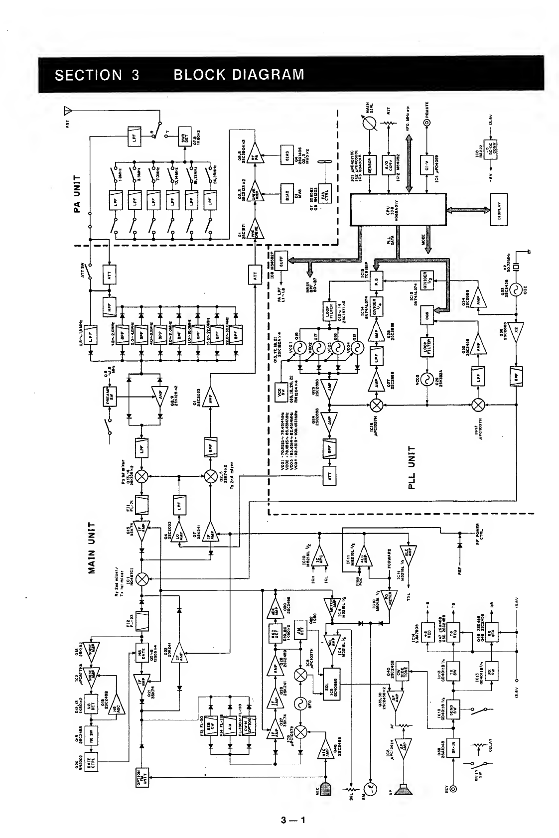
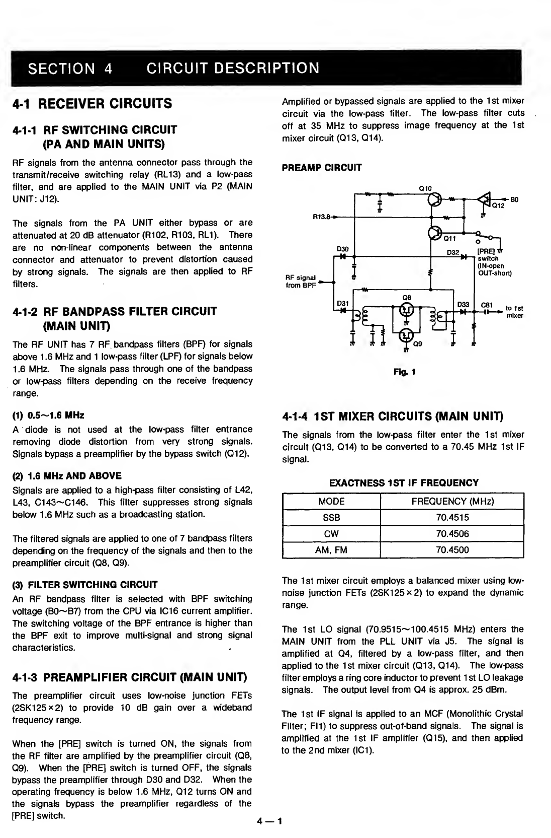
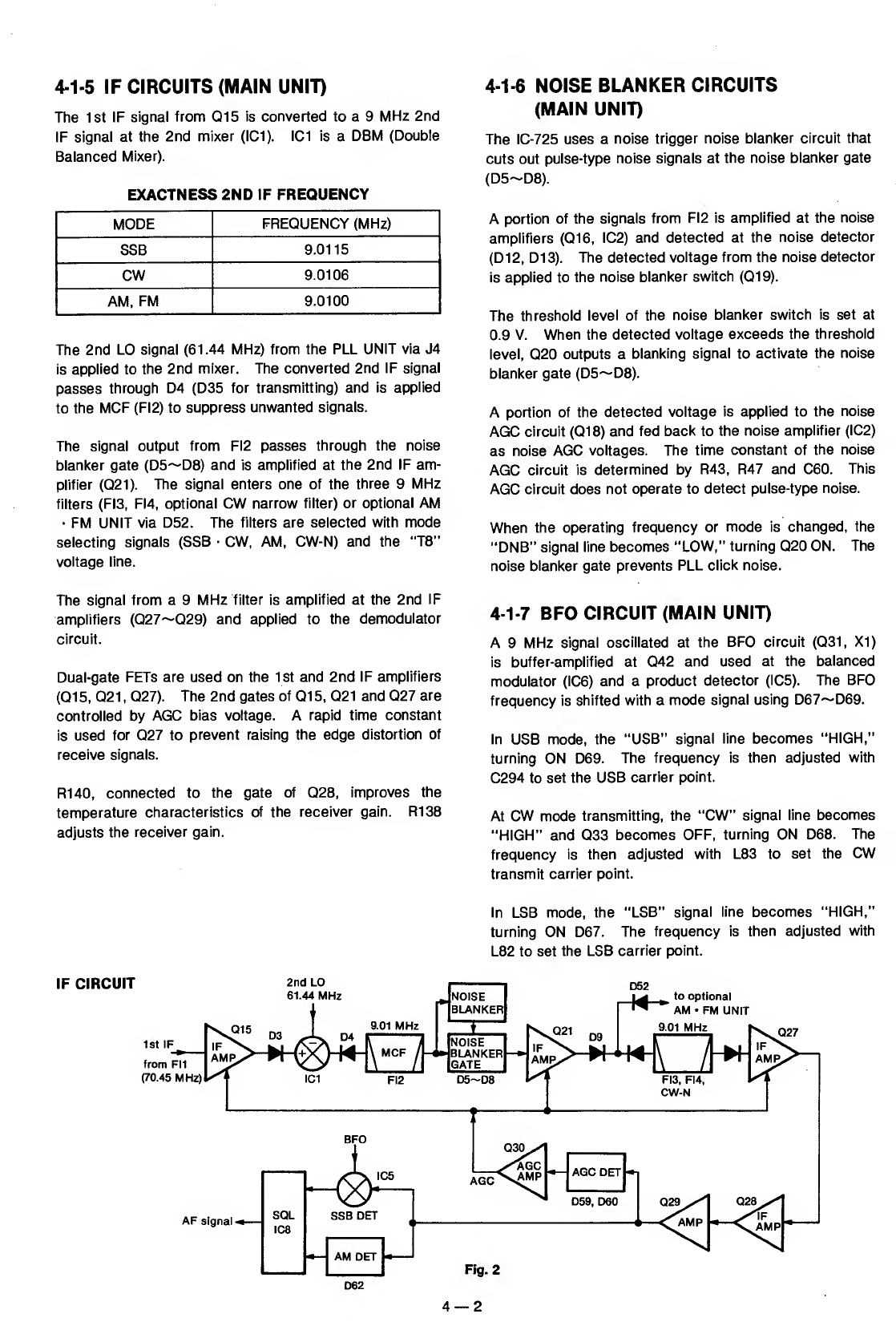
4-1-5 IF CIRCUITS (MAIN UNIT)
The 1st IF signal from Q15 is converted to a 9 MHz 2nd
IF signal at the 2nd mixer (iCI). IC1 is aDBM (Double
Balanced Mixer).
EXACTNESS 2ND IF FREQUENCY
MODE FREQUENCY (MHz)
SSB 9.0115
CW 9.0106
AM, FM 9.0100
The 2nd LO signal (61.44 MHz) from the PLL UNIT via J4
is applied to the 2nd mixer. The converted 2nd iF signal
passes through D4 (D35 for transmitting) and is applied
to the MCF (FI2) to suppress unwanted signals.
The signal output from FI2 passes through the noise
blanker gate (D5~D8) and is amplified at the 2nd IF am-
plifier (Q21). The signal enters one of the three 9MHz
filters (FIS, FI4, optional CW narrow filter) or optional AM
•FM UNIT via D52. The filters are selected with mode
selecting signals (SSB •CW, AM, CW-N) and the “T8”
voltage line.
The signal from a 9MHz filter is amplified at the 2nd IF
amplifiers (Q27~Q29) and applied to the demodulator
circuit.
Dual-gate FETs are used on the 1st and 2nd IF amplifiers
(Q1 5, Q21 ,Q27). The 2nd gates of Q1 5, Q21 and Q27 are
controlled by AGC bias voltage. Arapid time constant
is used for Q27 to prevent raising the edge distortion of
receive signals.
R140, connected to the gate of Q28, improves the
temperature characteristics of the receiver gain. R138
adjusts the receiver gain.
4-1-6 NOISE BLANKER CIRCUITS
(MAIN UNIT)
The IC-725 uses a noise trigger noise blanker circuit that
cuts out pulse-type noise signals at the noise blanker gate
(D5-D8).
Aportion of the signals from FI2 is amplified at the noise
amplifiers (Q16, IC2) and detected at the noise detector
(D1 2, D1 3). The detected voltage from the noise detector
is applied to the noise blanker switch (Q1 9).
The threshold level of the noise blanker switch is set at
0.9 V. When the detected voltage exceeds the threshold
level, Q20 outputs ablanking signal to activate the noise
blanker gate (D5~D8).
Aportion of the detected voltage is applied to the noise
AGC circuit (Q18) and fed back to the noise amplifier (IC2)
as noise AGC voltages. The time constant of the noise
AGC circuit is determined by R43, R47 and C60. This
AGC circuit does not operate to detect pulse-type noise.
When the operating frequency or mode is changed, the
“DNB” signal line becomes “LOW,” turning Q20 ON. The
noise blanker gate prevents PLL click noise.
4-1-7 BFO CIRCUIT (MAIN UNIT)
A9MHz signal oscillated at the BFO circuit (031, XI)
is buffer-amplified at Q42 and used at the balanced
modulator (IC6) and aproduct detector (ICS). The BFO
frequency is shifted with amode signal using D67~D69.
In USB mode, the “USB” signal line becomes “HIGH,”
turning ON D69. The frequency is then adjusted with
C294 to set the USB carrier point.
At CW mode transmitting, the “CW” signal line becomes
“HIGH” and 033 becomes OFF, turning ON D68. The
frequency is then adjusted with L83 to set the CW
transmit carrier point.
In LSB mode, the “LSB” signal line becomes “HIGH,”
turning ON D67. The frequency is then adjusted with
L82 to set the LSB carrier point.
IF CIRCUIT
062
4—2

BFO FREQUENCY IN EACH MODE
MODE FREQUENCY (MHz)
USB 9.0130
CW(Tx) 9.0106
LSB 9.0100
CW (Rx) 9.0098
AM NO OUTPUT
4-1-10 AF AMP CIRCUIT (MAIN UNIT)
The AF signal from the AF input mode selector switch is
applied to the AF preamplifier (Q35, Q36). The CW
sidetone signal is applied to Q36.
The output from the AF preamplifier is applied to the [AF]
control (FRONT UNIT, R1 b) and the 2.8 kHz cut-off active
low-pass filter (Q37). The AF signal is power-amplified at
IC9 to drive the speaker.
4-1-8 DEMODULATOR CIRCUITS
(MAIN UNIT)
The IC-725 has 2detector circuits, aproduct detector and
adiode detector to demodulate the SSB, CW signal and
AM signal respectively.
In SSB or CW mode, the 2nd IF signal from the IF amplifier
(Q29) is mixed with the BFO signal at the product detector
(ICS) to demodulate the 2nd IF signal into an AF signal.
The detected signal passes through the AF input mode
selector switch (ICS).
In AM mode, the 2nd IF signal from 029 passed through
Cl 21 is detected at D62 and passes through the AF input
mode selector switch (ICS).
4-1-11 AGC AND S-METER CIRCUIT
(MAIN UNIT)
The receiver gain is determined by the voltage on the AGC
line (030, collector). When strong signals are received,
the AGC circuit decreases the voltage on this line.
The IF signal from the IF amplifier (029) passes through
Cl 17, is detected at D59 and D60, and applied to the base
of 030. Atime constant (Cl 13, R120) is connected to
the AGC line that determines the AGC release time.
The time constant is controlled by the [AGC] switch. When
the [AGC] switch is pushed OUT, Cl 12 and R119 are
connected in parallel with the AGC line to obtain aslow
AGC release time.
4-1-9 AF INPUT MODE SELECTOR SWITCH
(MAIN UNIT)
The AF signal from adetector circuit or the optional AM
•FM UNIT is applied to the AF input mode selector switch
(ICS). ICS consists of 4analog switches and they are
selected with amode signal from IC15 and the squelch
control signal. The AF signal is applied to the AF amp
circuit.
ICS AF INPUT MODE SELECTOR SWITCH
MODE ACTIVATING
PIN NUMBERS CONTROL
PIN NUMBER
USB, CW 2-^1 13
AM 3^4 5
FM 10-^11 12
ANY MODES
(for S-meter) 9->8 6
The AGC bias voltage is applied to the differential amplifier
(IC4, pin 6) where the difference between the bias and
reference voltages is detected. The resulting S-meter
signal passes through the meter switching circuit (ICS)
and is then applied to the meter on the front panel. The
reference voltage is adjusted with R116. ICS pins 8and
9are connected inside the 1C in receiving.
The FM S-meter signal from the optional AM •FM UNIT is
applied to the meter switching circuit (ICS) via D57. The
signal is also applied to the squelch circuit (IC4 pin 2).

4-1-12 SQUELCH CIRCUIT (MAIN UNIT)
The squelch circuit mutes the audio output when the S-
meter signal is lower than the [SQL] control setting level.
The S-meter signal from IC4 pin 7is applied to the
comparator (IC4 pin 2) to be compared to athreshold
level controlled by the [SQL] control. The squelch control
signal is applied to control terminals of the AF input mode
selector switch (ICS).
When the S-meter signal is lower than the threshold level,
the comparator turns “HIGH" and then Q32 turns OFF to
deactivate the AF input mode selector switch. This
signal is applied to Q34, turning OFF the [RX] indicator
and is also applied to the [MIC] connector pin 4.
4-2 TRANSMITTER CIRCUITS
4-2-1 MIC AMPLIFIER (MAIN UNIT)
Audio signals from the [MIC] connector are applied to the
[MIC] control and amplified at the mic amplifier (Q45).
External modulation input from the [ACC(1)] socket pin 4
is also applied to Q45 via R255.
The AF signals from Q45 or CW keying signal is applied
to the balanced modulator (IC6). Q44 cuts the signals
from Q45 in CW or receiving.
4-2-2 BALANCED MODULATOR (MAIN UNIT)
Output signals from the mic amplifier or CW keying signal
are applied to the balanced modulator circuit (IC6) to be
converted to a 9 MHz IF signal using aBFO signal. The
BFO signal, buffer-amplified at Q42, is applied to ICS pin 7
as a carrier signal. ICS outputs adouble sideband signal
and passes through a 9 MHz filter to create an SSB
signal.
R177 and R179 adjust the balance level of ICS for
maximum carrier suppression. In CW mode, the CW
keying signal upsets the balance to create acarrier signal.
4-2-3 IF CIRCUITS (MAIN UNIT)
The 9MHz IF signal passes through one of the three
9MHz filters where unwanted sideband or out-of-band
signals are removed. The filters are selected with mode
selecting signals and the “T8” voltage line. The optional
CW narrow filter is not used in transmitting.
The resulting signal is amplified at Q22, and is then mixed
with the 2nd LO signal to be converted to a70.45 MHz IF
signal at IC1. IC1 is used in receiving and transmitting.
The FM signal from the optional AM •FM UNIT is amplified
at Q22 and is then applied to IC1
.
The 70.45 MHz IF signal is amplified at the IF amplifier
(Q7) and is then converted to the displayed frequency at
the balanced mixer (Q2, Q3).
The gates of the IF amplifiers (Q7, Q22) are controlled
by ALC bias voltage from the ALC circuit. R89, con-
nected to the gate of Q22, improves the temperature
characteristics of the transmitter gain. R85 adjusts the
transmitter gain.
4-2-4 RF CIRCUtTS (MAIN AND PA UNITS)
The converted signal from Q2 and Q3 is applied to the
bandpass filter where the unwanted LO signal emission is
reduced. The converted signal is amplified at Q1, and
is then applied to the PA UNIT via J11.
Incoming signals from the MAIN UNIT are amplified at the
predrive amplifier (Q1), drive amplifier (Q2, Q3) and power
amplifier (Q5, Q6) to obtain stable 100 WRF output
power. The predrive amplifier is aclass Aamplifier with a
Vcc of 13.8 V. The drive and power amplifiers are class
AB push-pull amplifiers with aVcc of 13.8 V. Astable bias
voltage is applied to these amplifiers. D1 controls abias
voltage to the drive amplifier. Q4, D2 and D3 supply a
bias voltage to the power amplifier.
A0.012 Qresistor (R26), inserted in the 13.8 VVcc line, is
provided for the Ic APC circuit. Avoltage generated at
both terminals of R26 is applied to the MAIN UNIT via
the “ICH” and “ICL” signal line.
Thermal switch SI and thermistor R32 detect the
temperature of Q6 and Q5 respectively, and control the
cooling fan speed.
TEMPERATURE °C (”F) Below 50
(122)
50~90
(122~194)
Above 90
(194)
THERMAL SWITCH (SI) OFF OFF ON
RESISTANCE OF R32 HIGH LOW LOW
COOLING RECEIVE STOP LOW HIGH
FAN SPEED transmit LOW HIGH
COOLING FAN CONTROL CIRCUIT

4-2-5 RF FILTER CIRCUIT (PA UNIT)
The PA UNIT has 6Chebyshev low-pass filters. The
signal from the power amplifier (Q5, Q6), applied to one of
the low-pass filters depending on the transmit frequency
range, suppresses high harmonic components.
The filter switching voltage, obtained at the PLL UNIT, is
applied to the PA UNIT via P7.
FREQUENCIES AND APPROPRIATE FILTERS
FILTER FREQUENCY RANGE (MHz)
LI Below 2
L2 2~4
L3 1CO
L4 8~15
L5 15~22
L6 22-30
The filtered signal passes through the SWR detector
circuit (L51) and is then applied to the antenna connector.
The forward signal from L51 is detected at D7 and applied
to the MAIN UNIT as the “FOR” voltage. The reflection
signal from L51 is detected at D8 and applied to the MAIN
UNIT as the “REF” voltage.
4-2-6 ALC CIRCUIT (MAIN UNIT)
The ALC (Auto Level Control) circuit stably controls the
RF output power using the [RF POWER] control.
The “FOR” voltage from the PA UNIT is applied to IC11
pin 2and IC10 pin 3. The “POC” voltage controlled
by the [RF PWR] control is also applied to IC1 1pin 3as
the reference voltage.
When the “FOR” voltage exceeds the “POC” voltage, ALC
bias voltage from IC11 pin 1controls the IF amplifiers
to reduce the output power until the “FOR” and “POC”
voltages are equalized.
In AM mode, IC11 operates as an averaging ALC
amplifier, because a capacitor on the optional AM •FM
UNIT (C51) is connected to the cathode of D76. Q54
turns ON and the “POC” voltage is shifted for 40 WAM
output power (maximum).
The ALC bias voltage from IC11 pin 1is also applied to
the inversion-amplifier (IC1 1pin 6) to control an intensity
of the [TX] indicator, showing the ALC level.
An external ALC input from the [ALC] jack is applied to
the buffer amplifier (Q53). ALC operation is identical to
that of the internal ALC.
4-2-7 APC CIRCUITS (MAIN UNIT)
The APC circuits protect the final transistors from high
SWR and excessive current. The “REF” voltage from
the PA UNIT is applied to Q56. When the “REF” voltage
exceeds the reference voltage, determined by R203 and
R204, Q56 turns ON and the “POC” voltage is shifted
for 12 Woutput power.
The “ICH” and “ICL” voltages are applied to the Ic APC
amplifier (IC10, pins 5and 6) and then to the ALC bias
voltage line to prevent excessive current flow.
4-2-8 CW KEYING CIRCUIT (MAIN UNIT)
When the CW key is closed, the “KEY” signal line
becomes “LOW.” Q38 outputs 8Vto control break-in
operation, sidetone signal and transmit signal.
When the [BK IN] switch is pushed IN, 8Vfrom Q38
charge C252 and 026 is turned ON, turning ON Q52.
Q52 grounds the SEND line for transmitting. The [DELAY]
control (R244) adjusts the transmit release delay time.
The 8Vfrom 038 charges C249 and D91 is turned OFF,
disconnecting C249 from 040. 040 then oscillates a
sidetone signal. R268 prevents sidetone click noise.
TTie 8Vfrom 038 is applied to atime constant and then to
the balanced modulator (IC6) to create acarrier signal.
R241 in the time constant adjusts atransmit delay timing
for 12 msec.
ALC CIRCUIT
4—5

While no CW transmit IF signal exists, Q39 and Q23 turn
the switching diode (D35) OFF to ensure transmit isolation.
4-2-9 OUTPUT POWER METER CIRCUITS
(MAIN UNIT)
The “FOR” voltage from the PA UNIT is applied to the Po
meter amplifier (1010 pin 3) and then to the meter. R189
and 0261 are used for peak power measurement.
4-2-10 T/R SWITCHING CIRCUIT
(MAIN UNIT)
When the PTT or [TRANSMITl switch is set to transmit,
IC13 pin 10 and 1013 pin 3are “LOW.” At this time,
049 turns ON, and 0Vis present on the “R8” voltage line.
050 turns OFF, and there is 8Vpresent on the “T8”
voltage line.
When the PTT or [TRANSMIT] switch is set to receive,
1013 pin 10 and 1013 pin 3are “HIGH.” At this time,
049 turns OFF, and 8VIs present on the “R8” voltage
line. 050 turns ON, and there-is 0Vpresent on the
“T8” voltage line.
When PLL data or the operating mode is changed, the
“DNB” signal line becomes “LOW,” turning OFF the T8 —
preventing unwanted transmission.
4-3 PLL CIRCUITS
4-3-1 GENERAL DESCRIPTION
The PLL UNIT generates a1st LO signal (70.951 5~
100.4515 MHz variable) and 2nd LO signal (61.44 MHz
fixed) used in the MAIN UNIT. The 10-725 uses adual loop
PLL system. Amain loop PLL uses 4VOO circuits for
all HF band coverage within 512 kHz steps. Asub loop
PLL uses aDOS (Direct Digital Synthesizer) system for
512 kHz coverage within 10 Hz steps. The DDS system
provides arapid lockup time and high quality frequency
oscillation.
4-3-2 REFERENCE OSCILLATOR CIRCUIT
(PLL UNIT)
A30.72 MHz reference frequency is produced by the
oscillator 033 and X2. The reference frequency, buffer-
amplified at 034, is divided by 2at 1015 and is then
applied to the PLL circuit as the PLL reference frequency.
The signal oscillated at 033 is multiplied by 2at Q36. The
resulting 61.44 MHz signal is filtered at the bandpass
filter and is then applied to the MAIN UNIT via P4 as
the 2nd LO signal.
4-3-3 MAIN LOOP (PLL UNIT)
The main loop uses aPLL 10 (1013) which contains a
programmable divider, phase detector, data shift register
and data latch circuits. The main loop generates
70.951 5~1 00.451 5MHz signals in 512 kHz steps.
Because the sub loop produces 10 Hz steps, the PLL
produces a30 MHz frequency range in 10 Hz steps.
The oscillated signal at one of the 4VOOs (015, 017,
019, 021 ;see Section 4-3-4 for details) is amplified at 023.
The signal is mixed with the sub loop output (fm:
62.05~62.561 99 MHz) at 1016. 023 is an isolator which
ensures that the mixer input does not affect the VCO
output.
The mixed signal is amplified at 027 and is then filtered
at the low-pass filter (L23~L25, 092, C93, C99~C103).
The filtered signal, amplified at 026, is divided by 4at
1014 and is then applied to the PLL 10 (IC13).
The phase of the divided signal at IC14, detected at
the PLL 10 (1013) using areference frequency (fpEp) of
512 kHz, is then output from pin 17. The 512 kHz
frequency is obtained from the reference oscillator (033).
30.72 MHz oscillated at 033, is divided by 2at IC15 and
divided by 30 at the programmable divider section of IC13.
The phase detected signal is then converted to the lock
voltage at the loop filter (Q12~Q14), and applied to the
VCO. Thus, the VCO output (PLL output) is locked to
produce stable oscillation.
The PLL oscillation frequency is obtained by the following
calculation:
fv =fLO +NTXfREF
fv :Main loop output
fto :Sub loop output
Nt :Dividing ratio from the CPU
ffiEp: Reference frequency (512 kHz)
4-3-4 VCO CIRCUIT (PLL UNIT)
The transceiver’s C/N ratio is determined by the VCO and
the loop filter. 4VCO circuits keep the low noise and
reduce spurious emissions. 016, 018, 020 and 022 are
VCO switches which select the operating VCO with
“VC01 ”~“VC04” lines.
4-3-5 SUB LOOP (PLL UNIT)
The sub loop uses the DDS system that generates
62.05~62.561 99 MHz signals in 10 Hz steps.
The oscillated signal at the VCO (029) is buffer-amplified at
030 and mixed with the 2nd LO signal (61.44 MHz) at
IC17. The resulting signal passes through the low-pass
filter, is amplified at 032, and is then applied to the DDS
UNIT.
The output pulse-type signal from the DDS UNIT passes
through the loop filter (R133, R134, C114, C115, L42)
where it is converted into aDC signal (lock voltage). The
lock voltage is applied to the VCO to lock the oscillating
frequency.
4—6

PLL CIRCUIT BLOCK DIAGRAM
Nt
MAIN LOOP
VC01
Q12-Q14
LOOP
FILTER
0/\vcoi
\^Jq17
fv: 70.951 5~
100.4515 MHz
/^^VC03
V^yoi9
AMP
Q23
fv
-r- LO AMP
Q24 .1St LO to
’main unit
1013
NPLL ^
t/ 1C
1014
V0O4
021
L-f,o: 8.5015-37.88951 MHz
DIVIDER
1/4
BUFFER
026 LPF
1016
AMP
027
15.36 MHz
r
—
1015
DIVIDER
1/2 DDS
fF
DATA
LOOP
FILTER
V005
0.61-1.12199 MHz
BUFFER
032 LPF 1017
BUFFER
034
SUB LOOP
REFERENOE
OSOILLATOR
X2
HD
30.72 MHz 033
MULTIPLIER
x2 036
f,o: 62.05-
62.56199 MHz
2nd LO
61.44 MHz
777 Fig. 6
4-4 LOGIC CIRCUITS
4-4-1 BAND SELECTION DATA (PLL UNIT)
To select the correct bandpass filter, the low-pass filter and
VCOs on the MAIN and PLL UNITS, the CPU outputs the
following data.
R29~R40 and D29~D35 convert the “B0”~“B7” signals
into aband voltage (0—7.5 V) for external equipment.
FREQUENOY (MHz) BPF BAND
VOLTAGE LPF VCO
0.5—1.599 BO 7.5 VLI
VC01
1.6-1.999 B1
2.0—3.999 B2 5.9 VL2
4.0-7.999 B3 5.0 VL3
8.0—10.999 B4 0.0 VL4 VC02
11.0-14.999 B5 4.1 V
15.0—21.999 B6 3.2 VL5 VC03
22.0-30.0 B7 2.2 VL6 VC04

4-4-2 CPU (PLL UNIT)
The CPU (IC8) contains an 8-bit CMOS CPU, 16k-byte ROM
and 256-byte RAM. The CPU controis operating
frequency, mode and the function display, etc. The
memory contents are stored in the CPU using alithium
backup battery for more than 5years.
The loom Cl-V network system allows that the IC-725 can
be remotely controlled by a personal computer using an
RS-232C signal line.
4-4-3 BIT CIRCUIT (PLL UNIT)
IC12 is an A/D converter which outputs 8-bit serial data
regarding analog input voltage. Avoltage, controlled by
the [RIT] control, is applied to IC12 pin 4and the resulting
serial data is applied to the CPU matrix Y4-» DB4.
4-4-4 KEY MATRIX
YO Y1 Y2 Y3 Y4
Fig. 7
44-5 PARALLEL/SERIAL CONVERTER
(PLL UNIT)
IC11 is aparallel/serial converter IC. Parallel data from
the CPU are converted into serial data to transfer the PLL
N-data, DDS N-data, data for LCD driver, etc.
When the power is turned ON, the CPU also outputs
programmable divider data and acontrol signal for
universal ports to the PLL IC (IC13).
4-5 REGULATOR CIRCUITS
Either 8, 5or -5 VDC are supplied from corresponding
regulator circuits. 8, 5and -5 VDC are regulated at
the following circuits using 13.8 VDC.
(1) 5VREGULATOR (PLL UNIT)
5VDC are regulated by the three-terminal voltage
regulator (IC1 0).
(2) 8VREGULATOR (MAIN UNIT)
8VDC are regulated by the three-terminal voltage
regulator (IC14).
(3) -5 VREGULATOR (PLL UNIT)
ICG generates anegative pulse-type voltage by converting
the DC input to AC voltages (approx. 6.7 kHz) as a
multivibrator. The voltage is rectified at D8 and D9,
regulated by a Zener diode (DIO) and Cl 3, and is then
applied to the MAIN UNIT.
4—7

SECTION 5MECHANICAL PARTS AND DISASSEMBLY

VR UNIT
(B1786C)

•FRAME DISASSEMBLY
ORDER
NO. DESCRIPTION QTY. LABEL
NUMBER ORDER
NO. DESCRIPTION QTY.
8110003270 Top cover 1MM 8930000720 Thread spacer (V) 4
@8110003280 Bottom cover 1EM 8930013990 610 Brake plate 1
®8930002900 Rubber foot (A) 2EM 8930014030 610 Brake pat 1
8930005790 Foot (A) 18930013940 610 Brake sheet 1
8930005800 Foot (B) 18810001110 PH BO M3x6 1
®8010001520 Stand (C) 11^ 8810005470 PH M2.6X14ZK 1
®8810005520 PH B1 M3X8ZK 48810001650 PH FTM3X6 9
®8810005540 PH B1 M4X10 28810001320 PH B1 M2.6X6 Ni 4
®8010007851 610 Chassis-1 .18510001330 79 shield case 1
8810001350 PH B1 M3x6 16 8510001340 79 shield case cover 1
8810002160 FH M3x5 16 MM 8510001060 Shield case 1
8810003670 ICOM screw A628510001740 Shield case cover 1
8810005510 FH M3X6ZK BS 16 MM 8510000881 194 VCO case-1 1
8210004670 610 Front panel (B) 1M^ 8510003460 194 VCO case cover (A) 1
11b!1 8610004640 Button K119[VFO] 1EM 8510000230 220 shield case 1
KM 8610004650 Button K1 19 (A) [SPLIT] 18510002200 VCO case 1
@8610004660 Button K1 19(B) [UP] 18510000881 194 VCO case-1 1
O8610004670 Button K1 19 (C) [MEMO] 1EM 8510002690 PA shield case (B) 1
8610004680 Button K119(0) [MW] 18510004360 PA shield case (B) cover (A) 1
,@8610004690 Button K1 19 (E) [DOWN] 1lo 8510005310 DOS shield case 1
@8610004700 Button K1 19(F) [FUNC] 18510005320 DDS shield case cover 1
8610004710 Button K1 19 (G) [RIT, TUNER] 2MM 2230000120 Switch [POWER] SDDSA3159A 1
8610004720 Button K120 [SSB, CW/N, AM/FM] 36510000190 Connector [M 1C] FM214-8SS (P) 1
^1 8610004730 Button K121 [kHz, MHz, BAND] 3MM 7600000100 Rotary encoder EC24B50B001 3A 1
@8610003850 Button K98 [TRANSMIT] 1i^M 7210000570 Variable resistor [RIT] 1
8610004741 Button K122-1 [LOCK] 16450000810 Connector [PHONES]
HLJ4306-01-3070 1
EM 8610004751 Button K123-1 [NB, ATT. PRE, AGC] 4
8610004760 Dial N104 (A)
(incl. rubber ring and screw) 17210001320 Variable resistor [AF/SQL]
RK1 24221 002DA 1
EM 8610004770 Knob N45C [AF, MIC] 2 7210001550 Variable resistor [MIC/RF PWR]
RK1 24221 0032A 1
8610000500 Knob N69 [SQL, RF PWR] 2
8610001560 Button K42 [POWER] 17210001530 Variable resistor [RIT]
RK09K1110AEGA 1
8610004780 Knob N87 (B) [RIT] 1
8010007860 610 Sub chassis 1IB 0910006330 Flexible cable P.C. Board B792 1
8930003200 Spacer (P) 1
Screw abbreviations PH: Pan head FH: Flat head BO, B1 .FT :Self-tapping screw ZK: Black Ni: Nickel
BS: Brass
5—2

PA UNIT
(B1790D)

•PA UNIT
Screw abbreviations PH: Pan head B1 :Self-tapping screw Ni: Nickel BS: Brass
•ACCESSORIES
LABa
NUHBER ORDER
NO. DESCRiPTiON QTY.
©Optional product DC power cable OPC-025 A1
@Optional product Hand microphone HM-12 1
@5210000080 Spare fuse FGB 20A 1
®5210000130 Spare fuse FGB 4A 1
8810005500 FH B1 M4X12CR 2
8810001600 PH ST M3 x6 4
Screw abbreviations PH :Pan head FH :Flat head
B1 ,ST: Self-tapping screw
5—4
Other manuals for IC-725
6
Table of contents
Other Icom Transceiver manuals

Icom
Icom IC-207H User manual

Icom
Icom IC-720 User manual

Icom
Icom IC-F1000 series User manual

Icom
Icom IC-281A User manual

Icom
Icom IC-A16 User manual

Icom
Icom iV86 Installation and operating instructions

Icom
Icom IC-U8S1 User manual

Icom
Icom IC-T2H User manual

Icom
Icom iC-7850 User manual

Icom
Icom D-STAR ID-31A; D-STAR ID-31E Setup guide