T1 CSU/DSU (V.35, 449, or 530)
8
2. Introduction
2.1 Overview
The T1 CSU/DSU is a high-speed T1 format processor with one of three interfaces for the DTE channel:
CCITT V.35, RS-449, or RS-530. It is capable of processing data at speeds from 56 kbps to 1.536 Mbps,
depending upon the format and density requirements of the application. It provides all the framing and density
requirements for data transmission across predefined network facilities, such as Accunet®.
The T1 CSU/DSU, because of its unique design, is able to accept timing information from any clock. Timing
information may be derived from the receive data, an external DTE, or from the internal crystal oscillator. The
T1 CSU/DSU has a series of selectable diagnostics that allow you to quickly and accurately troubleshoot the T1
CSU/DSU and the associated network.
The T1 CSU/DSU has a built-in CSU which complies with AT&T Publication 62411. This allows you to attach
the T1 CSU/DSU directly to the T1 circuit. This CSU can be enabled or disabled with a simple switch setting so
that the unit can act as a DSU or as a DSU/CSU. It can also be used as a high-speed line driver to extend high-
speed data circuits up to 6000 feet (1828.8 m) over shielded twisted-pair (STP) cable.
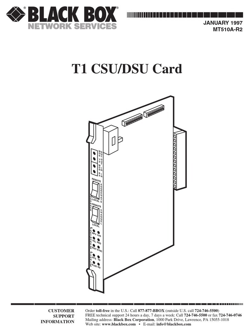
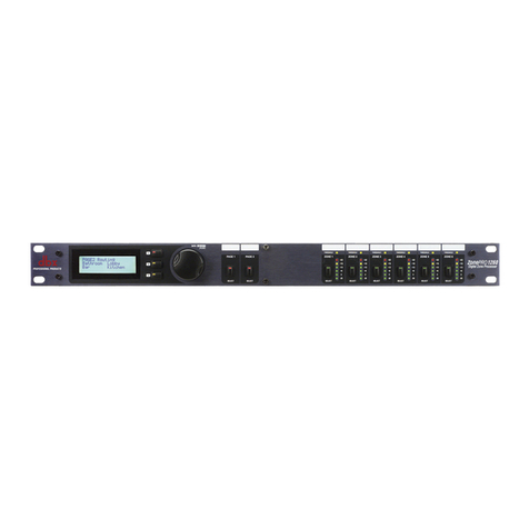
The T1 CSU/DSU contains all the controls and indicators necessary to configure, monitor, diagnose, and
operate the system. The front panel contains four bantam jack receptacles for network data monitoring and test
signal injection, loopback selection switches for aggregate and channel loopbacks, and a series of LEDs that
reflect the status of both the network and the DTE channel.
2.2 Bantam Jacks
The bantam jacks, located on the T1 CSU/DSU’s front panel, provide easy access to both monitor
the T1 service without interrupting the transmission of information or to inject a test signal to exercise the T1
circuit.
To monitor the T1 service, connect a test set to the T1 CSU/DSU via the Transmit Monitor (NET TX MON)
bantam jack and the Receive Monitor (NET RX MON) bantam jack. This allows the user to monitor the T1
service without interrupting the information flow.
To inject and receive a test signal across the T1 transmission facility, connect the test set into the IN (NET TX
IN) and OUT (NET RX OUT) bantam jacks. Then, place the T1 CSU/DSU in Remote Channel Loopback. In
this configuration, the operator can inject a known signal and receive it back via the network for testing
purposes. This is an interruptive test. Data integrity can not be guaranteed during this test.
2.3 Loopback Switches
There are two loopback switches on the T1 CSU/DSU’s front panel. Both switches allow the user to test
individual sections of the data transmission path. This ability to test these individual paths allows you to isolate,
diagnose, and then perform corrective action to resolve data transmission problems in the network.
