CIRCUIT DESIGN SLR-434M User manual

OPERATION GUIDE
OG_SLR-434M_v10e Circuit Design, Inc.
Embedded low power radio modem
SLR-434M
Smart RF modem
Operation Guide
Version 1.0 (Jan. 2018)
Circuit Design, Inc.
7557-1 Hotaka, Azumino, Nagano, Japan
Tel: 0263-82-1024
Fax: 0263-82-1016
e-mail: info@circuitdesign.jp
http://www.circuitdesign.jp

OPERATION GUIDE
OG_SLR-434M_v10e Circuit Design, Inc.
2
Contents
1. OVERVIEW ......................................................................................................................................... 3
2. FEATURES AND APPLICATIONS ...................................................................................................... 3
3. SPECIFICATIONS............................................................................................................................... 4
4. PART NAMES AND FUNCTIONS ....................................................................................................... 5
5. CONNECTION EXAMPLES FOR DIO TERMINALS .......................................................................... 8
6. APPEARANCE .................................................................................................................................... 9
7. COMMUNICATION FREQUENCY TABLE........................................................................................ 10
8. UART PORT COMMUNICATION SETTINGS....................................................................................11
9. SERIAL COMMUNICATION COMMANDS ....................................................................................... 12

OPERATION GUIDE
OG_SLR-434M_v10e Circuit Design, Inc.
3
1. Overview
The SLR-434M smart RF modem is a compact, easy to use, wireless modular RF modem for
embedding in other equipment.
In addition to conventional FSK mode communication, it also comes with a LoRa mode for ultra
long distance communication and low bit rate. With its superior receive sensitivity using LoRa
modulation, it achieves both specific low power output, with a line of sight communication range
of more than 10 kilometers.
Connection to an external microcomputer or a PC via a UART and our proprietary command
system fostered in the industry make it possible for you to easily transmit/receive data.
Also you can control up to 8 contacts.
2. Features and applications
Features
RED compliant (Plan)
Ultra long distance communication using the LoRa mode
Enhanced resistant to city noise and longer range compared with our earlier products
Select between FSK mode and LoRa mode
UART interface
Control of 8 contacts
Low power consumption enables battery powered operation
Compact size
Applications
Data transfer inside buildings, air conditioning control
Debris avalanche monitoring for debris barriers
Water level monitoring for river dams, opening and closing of water gates
Paddy field temperature and water level monitoring
Monitoring and control of greenhouse temperature and humidity
Transmission of sensor data from underground or inside manholes
Measurement and observation of the state of tunnels and bridges
Monitoring the state of electric fences
Monitoring the state of animal traps
Other IoT applications

OPERATION GUIDE
OG_SLR-434M_v10e Circuit Design, Inc.
4
3. Specifications
*All values are when the antenna connector is the 50 Ω terminal.
*Unless otherwise indicated, specified values are at a temperature of 25 °C ± 5 °C.
Item Specification
Applicable standard EN 300 220
Frequency channels 433.075 MHz to 434.7750 MHz (12.5 KHz step, 137 channels)
Frequency deviation ± 2 ppm or less
Antenna power 10 mW or less
Communication
method Half-duplex or one-way
Radio wave format F1D
Modulation*1LoRa or Binary FSK
Radio communication
speed
15 to 245 bps (Real speed using LoRa, depends on the spreading
factor)
4800 bps (FSK)
Receiver spurious
radiation -54 dBm or less
Receive sensitivity*2-133 dBm (LoRa 128 chip), -115 dBm or less (FSK),
PER 1% with the user data of 45 bytes or less
Carrier sensing
threshold -96 dBm (LoRa)
Operating temperature
range -30 to +70°C
Storage temperature
range -30 to +80°C
Recommended
operating voltage range 3.5 to 5.0 V
Warranted operating
voltage range 3.3 to 5.5 V
Operating current Tx: 29 mA (Typ) Rx: 17 mA (Typ) (Supply power = 5 V)
Antenna provided 1/4λ whip antenna (L=170 mm, gain 2.14 dBi or less)
Antenna connector SMA
Interface UART port
External dimensions 40 × 29 × 6.2 mm (±0.4) (Not including the antenna and
projections)
Weight 13 g
Soldering conditions Hand soldering
Soldering iron temp.: 350°C within 3 seconds
Note:
*1: When using the LoRa mode and moving around, the impact of the Doppler effect may make
communication impossible.
*2: Receive sensitivity performance is affected by the power supply and surrounding noise levels (floor noise
level). The approximate minimum level at which reception is possible is noise level +10 dB for FSK and -10
dB for LoRa. (Example: When the floor noise level is -110 dBm, reception is possible with FSK to about -
100 dBm and with LoRa to about -120 dBm). You can check the floor noise level with the @RA command
and the evaluation application (air monitor).

OPERATION GUIDE
OG_SLR-434M_v10e Circuit Design, Inc.
5
4. Part Names and Functions
Names
and
functions
I/O Content Internal equivalent circuit
TXD O A UART serial communication
terminal.
It sets the device and transmits
and receives data.
(Communication conditions:
19.2 kbps, Bits =8, Parity =
none, Stop = 1)
Serial data
Transmitter
RXD I Serial data
Receiver
RTS O
The UART control terminal.
When RTS = “Hi”, do not input
data.
Hardware flow
control output
terminal
CTS I
The UART control terminal.
When CTS = “Hi”, data is not
output.
(Set it to “Lo”.)
Hardware flow
control input
terminal
MODE I (Reserved)
Nothing should be connected to this terminal.
VCC
GND
TX-LED
RX-LED
DIO4
DIO5
DIO6
DIO7
DIO8
TXD
RXD
RTS
CTS
MODE
INI
RESET
DIO1
DIO2
DIO3
Antenna connector

OPERATION GUIDE
OG_SLR-434M_v10e Circuit Design, Inc.
6
INI I
With the power on, setting this terminal to
“Lo” for 3 s or more resets and restarts the
unit, and if the wireless communication mode
is binary mode, it enters the command mode.
For details about the wireless communication
mode, refer to the operation guide "SLR-434
Serial Communication".
Normally, when set to the wireless
communication mode, the settings are saved
automatically and are used as the initial
values next time the power is switched on.
However, after setting the binary mode, it is
not possible to receive commands, therefore
it is necessary to perform this task to return to
the command mode. When this task is
performed, "LORA CMD MODE" or "FSK CMD
MODE" is output from the TXD terminal after the
device restarts.
After reset and restart, the device is initialized
to the setting value saved by adding ‘/W’ to
commands such as chip number, frequency
channel.
RESET I
The CPU reset terminal (Lo active).
After reset and restart, the device is initialized
to the setting value saved by adding ‘/W’ to
commands such as chip number, frequency
channel.
DIO1 I/O Digital I/O pin 1. Input/output settings can be
made with commands.
DIO2 I/O Digital I/O pin 2. Input/output settings can be
made with commands.
DIO3
I/O
Digital I/O pin 3. Input/output
settings can be
made with
commands. DIO3
and DIO4 cannot
be set individually.
DIO4 Digital I/O pin 4.
DIO5
I/O
Digital I/O pin 5.
Input/output
settings can be
made with
commands.
DIO5 to DIO8
cannot be set
individually.
DIO6 Digital I/O pin 6.
DIO7 Digital I/O pin 7.
DIO8 Digital I/O pin 8.

OPERATION GUIDE
OG_SLR-434M_v10e Circuit Design, Inc.
7
RX-LED O
The reception monitor LED connection
terminal (Lo Active).
When a radio wave communication signal is
received, this terminal changes to “Lo” for
about 0.1 s.
TX-LED O
The transmission monitor LED connection
terminal (Lo Active).
When a radio wave communication signal is
sent, this terminal changes to “Lo”.
GND The ground terminal.
VCC The power supply terminal. Connect to a
stabilized DC+3.3 V to +5.5 V power supply.
Antenna
Connector I/O The connection pin for the antenna.
※The voltage range of the output terminal is 0 to Vcc [V].
Use the input terminal within the range Hi = 2.0 to Vcc [V], Lo = 0 to 0.6 [V]

OPERATION GUIDE
OG_SLR-434M_v10e Circuit Design, Inc.
8
5. Connection examples for DIO terminals
<When using the DIO terminals as input ports and connecting switches>
The DIO terminals are internally pulled-down and can be operated by connecting switches
between the DIO terminals and the VCC terminal as shown below (SW1 & SW2). The SW3 in the
circuit below shows an example of connecting a switch to the GND side with the signal level
inverted via a transistor.
Using long wiring between the DIO terminal and the switch may cause malfunction due to noise.
In that case, take measures such as externally pulling down with a resistor of a few to tens of kΩ.
<When using the DIO terminals as output ports and connecting loads>
The output current at the DIO terminal should be 5 mA or less.
Pay attention to the voltage drop due to the 330 Ω resistor inside the SLR-434M (see the
equivalent circuit above.)
A load of a few mA, such as LED, can be directly
driven as below.
Connecting a transistor or FET
Connecting a Photo Tr or PhotoMOS relay Connecting a relay

OPERATION GUIDE
OG_SLR-434M_v10e Circuit Design, Inc.
9
6. Appearance
Note: When designing circuit boards, take care to ensure space for the SMA connector
dimensions and screw fixture for connecting the antenna. (If the underside of the connector is
also the surface of the substrate, provide a notch or the like)
PCB

OPERATION GUIDE
OG_SLR-434M_v10e Circuit Design, Inc.
10
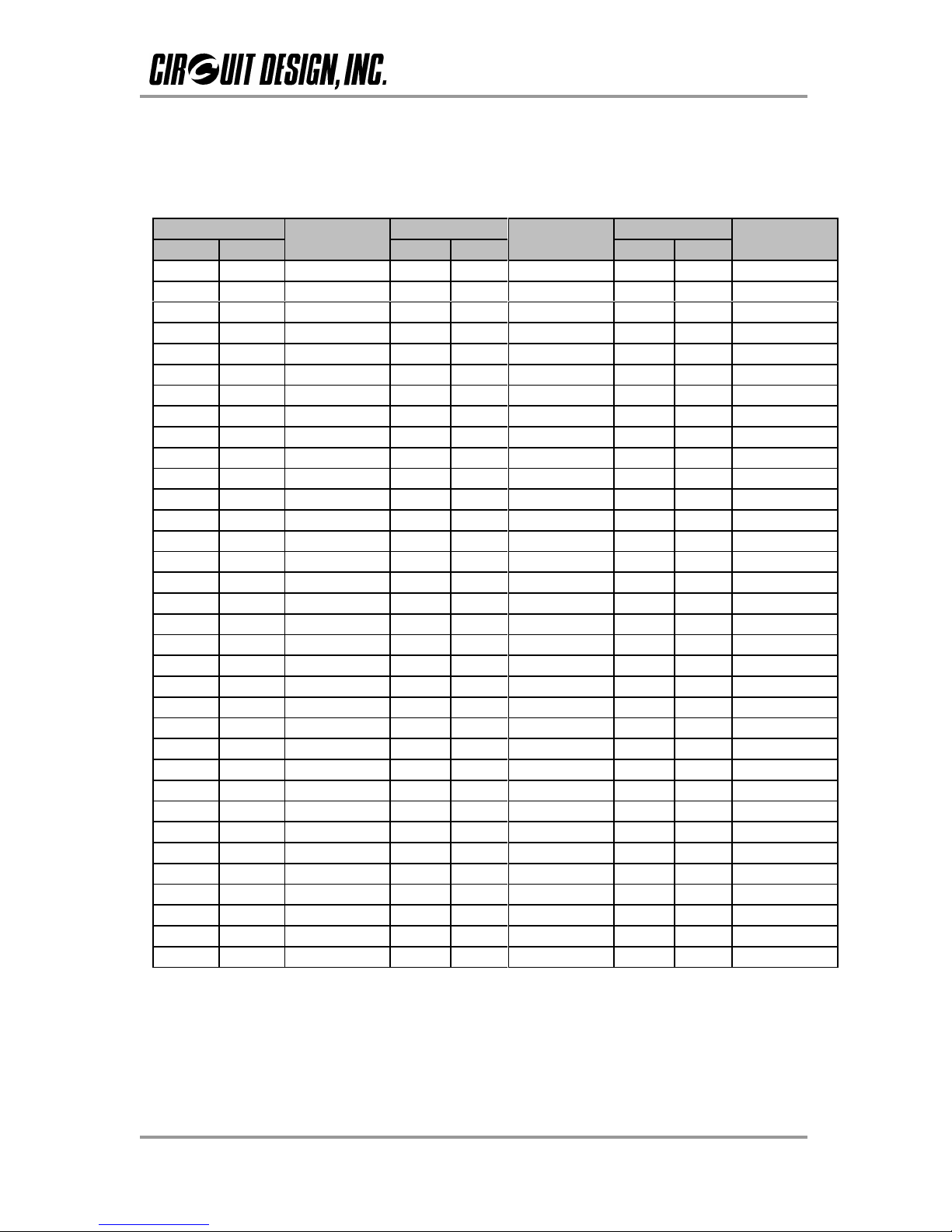
7. Communication frequency table
The frequencies used for radio communication are the 137 channels in the 434 MHz band shown in
the table below.
Channel Frequency Channel Frequency Channel Frequency
NO. HEX (MHz) NO. HEX (MHz) NO. HEX (MHz)
0 00 433.0750 34 22 433.5000 68 44 433.9250
1 01 433.0875 35 23 433.5125 69 45 433.9375
2 02 433.1000 36 24 433.5250 70 46 433.9500
3 03 433.1125 37 25 433.5375 71 47 433.9625
4 04 433.1250 38 26 433.5500 72 48 433.9750
5 05 433.1375 39 27 433.5625 73 49 433.9875
6 06 433.1500 40 28 433.5750 74 4A 434.0000
7 07 433.1625 41 29 433.5875 75 4B 434.0125
8 08 433.1750 42 2A 433.6000 76 4C 434.0250
9 09 433.1875 43 2B 433.6125 77 4D 434.0375
10 0A 433.2000 44 2C 433.6250 78 4E 434.0500
11 0B 433.2125 45 2D 433.6375 79 4F 434.0625
12 0C 433.2250 46 2E 433.6500 80 50 434.0750
13 0D 433.2375 47 2F 433.6625 81 51 434.0875
14 0E 433.2500 48 30 433.6750 82 52 434.1000
15 0F 433.2625 49 31 433.6875 83 53 434.1125
16 10 433.2750 50 32 433.7000 84 54 434.1250
17 11 433.2875 51 33 433.7125 85 55 434.1375
18 12 433.3000 52 34 433.7250 86 56 434.1500
19 13 433.3125 53 35 433.7375 87 57 434.1625
20 14 433.3250 54 36 433.7500 88 58 434.1750
21 15 433.3375 55 37 433.7625 89 59 434.1875
22 16 433.3500 56 38 433.7750 90 5A 434.2000
23 17 433.3625 57 39 433.7875 91 5B 434.2125
24 18 433.3750 58 3A 433.8000 92 5C 434.2250
25 19 433.3875 59 3B 433.8125 93 5D 434.2375
26 1A 433.4000 60 3C 433.8250 94 5E 434.2500
27 1B 433.4125 61 3D 433.8375 95 5F 434.2625
28 1C 433.4250 62 3E 433.8500 96 60 434.2750
29 1D 433.4375 63 3F 433.8625 97 61 434.2875
30 1E 433.4500 64 40 433.8750 98 62 434.3000
31 1F 433.4625 65 41 433.8875 99 63 434.3125
32 20 433.4750 66 42 433.9000 100 64 434.3250
33 21 433.4875 67 43 433.9125 101 65 434.3375

OPERATION GUIDE
OG_SLR-434M_v10e Circuit Design, Inc.
11
Channel Frequency Channel Frequency Channel Frequency
NO. HEX (MHz) NO. HEX (MHz) NO. HEX (MHz)
102 66 434.3500 114 72 434.5000 126 7E 434.6500
103 67 434.3625 115 73 434.5125 127 7F 434.6625
104 68 434.3750 116 74 434.5250 128 80 434.6750
105 69 434.3875 117 75 434.5375 129 81 434.6875
106 6A 434.4000 118 76 434.5500 130 82 434.7000
107 6B 434.4125 119 77 434.5625 131 83 434.7125
108 6C 434.4250 120 78 434.5750 132 84 434.7250
109 6D 434.4375 121 79 434.5875 133 85 434.7375
110 6E 434.4500 122 7A 434.6000 134 86 434.7500
111 6F 434.4625 123 7B 434.6125 135 87 434.7625
112 70 434.4750 124 7C 434.6250 136 88 434.7750
113 71 434.4875 125 7D 434.6375
※*The channel is set to No. 74 (434.000 MHz) for shipment.
※*If you intend to use several SLR-434M units in the same area, use a channel plan that takes into
account radio interference due to third-order intermodulation.
Circuit Design provides a computational tool on our website for creating channel plans that avoid
interference due to third-order intermodulation. Calculation tool:
http://www.cdt21.com/resources/siryo6.asp
8. UART port communication settings
The serial communication conditions for the UART port of this product are as follows.
Communicatio
n speed 19,200 bps
Fixed value
Cannot be
changed.
Data 8-bit
Parity None
Stop 1-bit
Flow control Hardware: RTS/CTS pin
(Software flow: Xon/Xoff is not used)
(The RTS output terminal is normally Lo. When the CTS input terminal is “Hi”, UART data is not
output)
Note: The UART serial communication terminals (TXD/RXD/RTS/CTS) cannot be connected
directly to a PC or other Com port because the signal level and logic is different.

OPERATION GUIDE
OG_SLR-434M_v10e Circuit Design, Inc.
12
9. Serial communication commands
The table below shows examples of the basic commands and responses.
See the operation guide "SLR-434M Serial Communication" for details and other command values.
Item Commands Value
(hex) Options Response example Content (with a response example)
Radio
communication
mode setting @MO
00
*WR=PS
*MO=00
FSK BIN MODE
Sets the
communication mode
to FSK binary mode.
The value set is
automatically saved and
the device restarts.
A character string that
indicates the mode of
the response example
is output after
restarting.
In the binary mode, it is
not possible to receive
any commands,
therefore it is necessary
to set the INI terminal to
Low for more than 3
seconds to return to the
command mode.
01
*WR=PS
*MO=01
FSK CMD MODE
Sets the
communication mode
to FSK command
mode.
02
*WR=PS
*MO=02
LORA BIN MODE
Sets the
communication mode
to LoRa binary mode.
03
*WR=PS
*MO=03
LORA CMD MODE
Sets the
communication mode
to LoRa command
mode.
LoRa
Number of chips
setting
@SF 00
*SF00
Sets the number of chips with LoRa to 128 chips.
/W *WR=PS
*SF00
Channel setting @CH 4A
*CH1B Sets the communication frequency to 434.000
MHz (See '7.Communication frequency table'.)
/W *WR=PS
*CH1B
ID setting
(Equipment,
Target station,
Group ID)
@EI
@DI
@GI
0A
(With Equipment ID)
*EI=0A Sets the Equipment ID (local station) to “0A”
(Sets the ID for identifying each radio station and
the other party in communication.)
/W *WR=PS
*EI=0A
Transmit data @DT 05abcde *DT=05 Sends the 5-byte data “abcde”.
Receive data *DR=05abcde Indicates that the 5-byte data “abcde” was
received.
RSSI acquisition
for the last data
received.
@RS *RS=-100dBm
Acquires the RSSI level (strength of the radio
waves of the received signal) for the last data
received.
Current RSSI
acquisition @RA *RA=-120dBm Acquires the current RSSI level (radio wave
strength) of the channel set.
Contact function
IO setting @PS 0F
*PS =0F Sets contacts DIO1 to DIO4 as input ports and
DIO5 to DIO8 as output ports.
/W *WR=PS
*PS=0F
Contact state
check and
setting
@PO 10
*PO=10 Sets contact DIO5 to Hi. Acquires the status if it
is the input port.
/W *WR=PS
*PO=10
Target station
contact state
check and
setting
@PT
*PT=10
*PR=040280
Acquires the contact information of the target
station.
(“* PR =...” shows the response from the target
station.)
20 *PT=20
*PR=040220
Sets the contact status of the target station.
(“* PR =...” shows the response from the target
station.)
Contact
communication
mode setting
@PM 01
*PM=01 If the status of the contacts set to input changes,
the contact information is transmitted
automatically (once).
If the target station receives this signal, the
status of the corresponding contact output
changes.
/W *WR=PS
*PM=01

OPERATION GUIDE
OG_SLR-434M_v10e Circuit Design, Inc.
13
After command + value + data (optional), add the line feed code ‘CR’ ‘LF’.
If you omit value + data, you can check the content of the current settings.
If the optional ‘/W’ is added, the setting value is saved, and it becomes the initial value next time the
power is switched on.

OPERATION GUIDE
OG_SLR-434M_v10e Circuit Design, Inc.
14
Important notice
Customers are advised to consult with Circuit Design sales representatives before ordering.
Circuit Design believes the provided information is accurate and reliable. However, Circuit Design
reserves the right to make changes to this product without notice.
Circuit Design products are neither designed nor intended for use in life support applications where
malfunction can reasonably be expected to result in significant personal injury to the user. Any use
of Circuit Design products in such safety-critical applications is understood to be fully at the risk of
the customer and the customer must fully indemnify Circuit Design, Inc for any damages resulting
from any improper use.
As the radio module communicates using electronic radio waves, there are cases where
transmission will be temporarily cut off due to the surrounding environment and method of usage.
The manufacturer is exempt from all responsibility relating to resulting harm to personnel or
equipment and other secondary damage.
The manufacturer is exempt from all responsibility relating to secondary damage resulting from the
operation, performance and reliability of equipment connected to the radio module.
Copyright
All rights in this operation guide are owned by Circuit Design, Inc. No part of this document may be
copied or distributed in part or in whole without the prior written consent of Circuit Design, Inc.
Cautions
Do not use the equipment within the vicinity of devices that may malfunction as a result of electronic
radio waves from the radio module.
Communication performance will be affected by the surrounding environment, so communication
tests should be carried out before actual use.
Ensure that the power supply for the radio module is within the specified rating. Short circuits and
reverse connections may result in overheating and damage and must be avoided at all costs.
Ensure that the power supply has been switched off before attempting any wiring work.
The case is connected to the GND terminal of the internal circuit, so do not make contact between
the '+' side of the power supply terminal and the case.
When batteries are used as the power source, avoid short circuits, recharging, dismantling, and
pressure. Failure to observe this caution may result in the outbreak of fire, overheating and damage
to the equipment. Remove the batteries when the equipment is not to be used for a long period of
time. Failure to observe this caution may result in battery leaks and damage to the equipment.
Do not use this equipment in vehicles with the windows closed, in locations where it is subject to
direct sunlight, or in locations with extremely high humidity.
The radio module is neither waterproof nor splash proof. Ensure that it is not splashed with soot or
water. Do not use the equipment if water or other foreign matter has entered the case.
Do not drop the radio module or otherwise subject it to strong shocks.
Do not subject the equipment to condensation (including moving it from cold locations to locations
with a significant increase in temperature.)
Do not use the equipment in locations where it is likely to be affected by acid, alkalis, organic agents
or corrosive gas.
Do not bend or break the antenna. Metallic objects placed in the vicinity of the antenna will have a
great effect on communication performance. As far as possible, ensure that the equipment is placed
well away from metallic objects.
The GND for the radio module will also affect communication performance. If possible, ensure that
the case GND and the circuit GND are connected to a large GND pattern.
Warnings
Do not take apart or modify the equipment.
Do not remove the product label (the label attached to the upper surface of the module.) Using a
module from which the label has been removed is prohibited.
Copyright 2018, Circuit Design, Inc.

OPERATION GUIDE
OG_SLR-434M_v10e Circuit Design, Inc.
15
Revision History
Version Date Description Remark
0.91 Feb. 2017 Provisional Edition
1.0 Jan. 2018
The copyright of this manual belongs to Circuit Design, Inc. Reproduction, duplication or
modification of part or all of this manual without permission is prohibited.
Table of contents
Other CIRCUIT DESIGN Radio Modem manuals