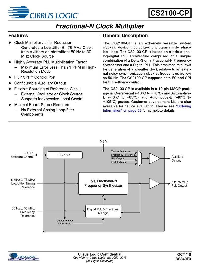
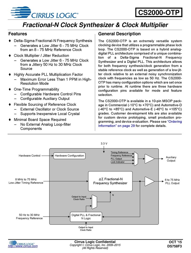
Cirrus Logic CS2200-CP User manual

Cirrus Logic Confidential
Copyright Cirrus Logic, Inc. 2009–2015
(All Rights Reserved)
http://www.cirrus.com
Fractional-N Frequency Synthesizer
Features
Delta-Sigma Fractional-N Frequency Synthesis
– Generates a Low Jitter 6 - 75 MHz Clock
from an 8 - 75 MHz Reference Clock
Highly Accurate PLL Multiplication Factor
– Maximum Error Less Than 1 PPM
I²C / SPI™ Control Port
Configurable Auxiliary Output
– Buffered Reference Clock
– PLL Lock Indication
– Duplicate PLL Output
Flexible Sourcing of Reference Clock
– External Oscillator or Clock Source
– Supports Inexpensive Local Crystal
Minimal Board Space Required
– No External Analog Loop-filter
Components
General Description
The CS2200-CP is an extremely versatile system clock-
ing device that utilizes a programmable phase lock loop.
The CS2200-CP is based on an analog PLL architec-
ture comprised of a Delta-Sigma Fractional-N
Frequency Synthesizer. This architecture allows for fre-
quency synthesis and clock generation from a stable
reference clock.
The CS2200-CP supports both I²C and SPI for full soft-
ware control.
The CS2200-CP is available in a 10-pin MSOP package
in Commercial (-10°C to +70°C) and Automotive-D
(-40°C to +85°C) and Automotive-E (-40°C to +105°C)
grades.
Customer development kits are also available for device
evaluation. Please see “Ordering Information” on
page 25 for complete details.
I²C / SPI Auxiliary
Output
6 to 75 MHz
PLL Output
3.3 V
I²C/SPI Software
Control
8 MHz to 75 MHz
Low-Jitter Timing
Reference
Output to Input
Clock Ratio
N
Timing Reference
PLL Output
PLL Lock Indicator
Fractional-N
Divider
Voltage Controlled
Oscillator
Internal
Loop Filter
Phase
Comparator
Delta-Sigma
Modulator
OCT '15
DS759F3
CS2200-CP

CS2200-CP
2DS759F3
TABLE OF CONTENTS
1. PIN DESCRIPTION ................................................................................................................................. 4
2. TYPICAL CONNECTION DIAGRAM ..................................................................................................... 5
3. CHARACTERISTICS AND SPECIFICATIONS ...................................................................................... 6
RECOMMENDED OPERATING CONDITIONS .................................................................................... 6
ABSOLUTE MAXIMUM RATINGS ........................................................................................................ 6
DC ELECTRICAL CHARACTERISTICS ................................................................................................ 6
AC ELECTRICAL CHARACTERISTICS ................................................................................................ 7
CONTROL PORT SWITCHING CHARACTERISTICS- I²C FORMAT ................................................... 8
CONTROL PORT SWITCHING CHARACTERISTICS - SPI FORMAT ................................................. 9
4. ARCHITECTURE OVERVIEW ............................................................................................................. 10
4.1 Delta-Sigma Fractional-N Frequency Synthesizer ......................................................................... 10
5. APPLICATIONS ................................................................................................................................... 11
5.1 Timing Reference Clock Input ........................................................................................................ 11
5.1.1 Internal Timing Reference Clock Divider ............................................................................... 11
5.1.2 Crystal Connections (XTI and XTO) ...................................................................................... 12
5.1.3 External Reference Clock (REF_CLK) .................................................................................. 12
5.2 Output to Input Frequency Ratio Configuration ............................................................................. 12
5.2.1 User Defined Ratio (RUD) ..................................................................................................... 12
5.2.2 Ratio Modifier (R-Mod) .......................................................................................................... 13
5.2.3 Effective Ratio (REFF) .......................................................................................................... 13
5.2.4 Ratio Configuration Summary ............................................................................................... 14
5.3 PLL Clock Output ........................................................................................................................... 14
5.4 Auxiliary Output .............................................................................................................................. 15
5.5 Clock Output Stability Considerations ............................................................................................ 15
5.5.1 Output Switching ................................................................................................................... 15
5.5.2 PLL Unlock Conditions .......................................................................................................... 15
5.6 Required Power Up Sequencing .................................................................................................... 16
6. SPI / I²C CONTROL PORT ................................................................................................................... 16
6.1 SPI Control ..................................................................................................................................... 16
6.2 I²C Control ...................................................................................................................................... 16
6.3 Memory Address Pointer ............................................................................................................... 18
6.3.1 Map Auto Increment .............................................................................................................. 18
7. REGISTER QUICK REFERENCE ........................................................................................................ 18
8. REGISTER DESCRIPTIONS ................................................................................................................ 19
8.1 Device I.D. and Revision (Address 01h) ........................................................................................ 19
8.1.1 Device Identification (Device[4:0]) - Read Only ..................................................................... 19
8.1.2 Device Revision (Revision[2:0]) - Read Only ........................................................................ 19
8.2 Device Control (Address 02h) ........................................................................................................ 19
8.2.1 Unlock Indicator (Unlock) - Read Only .................................................................................. 19
8.2.2 Auxiliary Output Disable (AuxOutDis) ................................................................................... 19
8.2.3 PLL Clock Output Disable (ClkOutDis) .................................................................................. 20
8.3 Device Configuration 1 (Address 03h) ........................................................................................... 20
8.3.1 R-Mod Selection (RModSel[2:0]) ...........................................................................................20
8.3.2 Auxiliary Output Source Selection (AuxOutSrc[1:0]) ............................................................. 20
8.3.3 Enable Device Configuration Registers 1 (EnDevCfg1) ........................................................ 21
8.4 Global Configuration (Address 05h) ............................................................................................... 21
8.4.1 Device Configuration Freeze (Freeze) .................................................................................. 21
8.4.2 Enable Device Configuration Registers 2 (EnDevCfg2) ........................................................ 21
8.5 Ratio (Address 06h - 09h) .............................................................................................................. 21
8.6 Function Configuration 1 (Address 16h) ........................................................................................ 22
8.6.1 AUX PLL Lock Output Configuration (AuxLockCfg) .............................................................. 22
8.6.2 Reference Clock Input Divider (RefClkDiv[1:0]) .................................................................... 22

CS2200-CP
DS759F3 3
8.7 Function Configuration 2 (Address 17h) ........................................................................................ 22
8.7.1 Enable PLL Clock Output on Unlock (ClkOutUnl) ................................................................. 22
9. CALCULATING THE USER DEFINED RATIO .................................................................................... 23
9.1 12.20 Format .................................................................................................................................. 23
10. PACKAGE DIMENSIONS .................................................................................................................. 24
THERMAL CHARACTERISTICS ......................................................................................................... 24
11. ORDERING INFORMATION .............................................................................................................. 25
12. REFERENCES .................................................................................................................................... 25
13. REVISION HISTORY .......................................................................................................................... 26
LIST OF FIGURES
Figure 1. Typical Connection Diagram ........................................................................................................ 5
Figure 2. Control Port Timing - I²C Format .................................................................................................. 8
Figure 3. Control Port Timing - SPI Format (Write Only) ............................................................................ 9
Figure 4. Delta-Sigma Fractional-N Frequency Synthesizer ..................................................................... 10
Figure 5. Internal Timing Reference Clock Divider ................................................................................... 11
Figure 6. REF_CLK Frequency vs. a Fixed CLK_OUT ............................................................................. 11
Figure 7. External Component Requirements for Crystal Circuit .............................................................. 12
Figure 8. Ratio Feature Summary ............................................................................................................. 14
Figure 9. PLL Clock Output Options ......................................................................................................... 14
Figure 10. Auxiliary Output Selection ........................................................................................................ 15
Figure 11. Control Port Timing in SPI Mode ............................................................................................. 17
Figure 12. Control Port Timing, I²C Write .................................................................................................. 17
Figure 13. Control Port Timing, I²C Aborted Write + Read .......................................................................17
LIST OF TABLES
Table 1. Ratio Modifier .............................................................................................................................. 13
Table 2. Example 12.20 R-Values ............................................................................................................ 23

CS2200-CP
4DS759F3
1. PIN DESCRIPTION
Pin Name # Pin Description
VD 1 Digital Power (Input) - Positive power supply for the digital and analog sections.
GND 2 Ground (Input) - Ground reference.
CLK_OUT 3 PLL Clock Output (Output) - PLL clock output.
AUX_OUT 4Auxiliary Output (Output) - This pin outputs a buffered version of one of the input or output clocks,
or a status signal, depending on register configuration.
TST_IN 5Test Input (Input) - This pin is for factory test purposes and must be connected to GND for proper
operation.
XTO
XTI/REF_CLK
6
7
Crystal Connections (XTI/XTO) / Timing Reference Clock Input (REF_CLK) (Input/Output) -
XTI/XTO are I/O pins for an external crystal which may be used to generate the low-jitter PLL input
clock. REF_CLK is an input for an externally generated low-jitter reference clock.
AD0/CS 8Address Bit 0 (I²C) / Control Port Chip Select (SPI) (Input) - AD0 is a chip address pin in I²C
Mode. CS is the chip select signal in SPI Mode.
SCL/CCLK 9Control Port Clock (Input) - SCL/CCLK is the serial clock for the serial control port in I²C and SPI
mode.
SDA/CDIN 10 Serial Control Data (Input/Output) - SDA is the data I/O line in I²C Mode. CDIN is the input data
line for the control port interface in SPI Mode.
1
2
3
4
56
7
8
9
10
XTO
CLK_OUT
GND
VD
XTI/REF_CLK
AD0/CS
SCL/CCLK
SDA/CDIN
AUX_OUT
TST_IN

CS2200-CP
DS759F3 5
2. TYPICAL CONNECTION DIAGRAM
2
1
GND
SCL/CCLK
SDA/CDIN
2 k
XTI/REF_CLK
TST_IN
XTO
CLK_OUT
AUX_OUT
0.1 µF
VD
+3.3 V
Notes:
1. Resistors
required for I2C
operation. 2 k
AD0/CS
Low-Jitter
Timing Reference
System MicroController
1 µF
Note1
1
or
2
REF_CLK
XTO
XTI
XTO
or
40 pF
x
40 pF
Crystal
To circuitry which requires
a low-jitter clock
N.C.
To other circuitry or
Microcontroller
Figure 1. Typical Connection Diagram
CS2200-CP

CS2200-CP
6DS759F3
3. CHARACTERISTICS AND SPECIFICATIONS
RECOMMENDED OPERATING CONDITIONS
GND = 0 V; all voltages with respect to ground. (Note 1)
Notes: 1. Device functionality is not guaranteed or implied outside of these limits. Operation outside of these limits
may adversely affect device reliability.
ABSOLUTE MAXIMUM RATINGS
GND = 0 V; all voltages with respect to ground.
CAUTION: Stresses beyond “Absolute Maximum Ratings” levels may cause permanent damage to the device.
These levels are stress ratings only, and functional operation of the device at these or any other condi-
tions beyond those indicated in Section 3. on page 7 is not implied. Exposure to absolute maximum
rating conditions for extended periods may affect device reliability.
Notes: 2. The maximum over/under voltage is limited by the input current except on the power supply pin.
DC ELECTRICAL CHARACTERISTICS
Test Conditions (unless otherwise specified): VD = 3.1 V to 3.5 V; TA= -10°C to +70°C (Commercial Grade);
TA= -40°C to +85°C (Automotive-D Grade); TA= -40°C to +105°C (Automotive-E Grade)
Notes: 3. To calculate the additional current consumption due to loading (per output pin), multiply clock output
frequency by load capacitance and power supply voltage. For example, fCLK_OUT (49.152 MHz) * CL
(15 pF) * VD (3.3 V) = 2.4 mA of additional current due to these loading conditions on CLK_OUT.
Parameters Symbol Min Typ Max Units
DC Power Supply VD 3.1 3.3 3.5 V
Ambient Operating Temperature (Power Applied)
Commercial Grade
Automotive-D Grade
Automotive-E Grade
TAC
TAD
TAE
-10
-40
-40
-
-
-
+70
+85
+105
°C
°C
°C
Parameters Symbol Min Max Units
DC Power Supply VD -0.3 6.0 V
Input Current IIN -±10mA
Digital Input Voltage (Note 2)V
IN -0.3 VD + 0.4 V
Ambient Operating Temperature (Power Applied) TA-55 125 °C
Storage Temperature Tstg -65 150 °C
Parameters Symbol Min Typ Max Units
Power Supply Current - Unloaded (Note 3)I
D-1218mA
Power Dissipation - Unloaded (Note 3)P
D-4060mW
Input Leakage Current IIN --±10µA
Input Capacitance IC-8-pF
High-Level Input Voltage VIH 70% - - VD
Low-Level Input Voltage VIL --30%VD
High-Level Output Voltage (IOH = -1.2 mA) VOH 80% - - VD
Low-Level Output Voltage (IOH = 1.2 mA) VOL --20%VD

CS2200-CP
DS759F3 7
AC ELECTRICAL CHARACTERISTICS
Test Conditions (unless otherwise specified): VD = 3.1 V to 3.5 V; TA= -10°C to +70°C (Commercial Grade);
TA= -40°C to +85°C (Automotive-D Grade); TA= -40°C to +105°C (Automotive-E Grade); CL=15pF.
Notes: 4.
5. fCLK_OUT is ratio-limited when fCLK_IN is below 72 Hz.
6. fCLK_OUT = 24.576 MHz; Sample size = 10,000 points; AuxOutSrc[1:0] =11.
7. In accordance with AES-12id-2006 section 3.4.2. Measurements are Time Interval Error taken with 3rd
order 100 Hz to 40 kHz bandpass filter.
8. In accordance with AES-12id-2006 section 3.4.1. Measurements are Time Interval Error taken with 3rd
order 100 Hz Highpass filter.
9. The frequency accuracy of the PLL clock output is directly proportional to the frequency accuracy of the
reference clock.
Parameters Symbol Conditions Min Typ Max Units
Crystal Frequency
Fundamental Mode XTAL
fXTAL RefClkDiv[1:0] = 10
RefClkDiv[1:0] = 01
RefClkDiv[1:0] = 00
8
16
32
-
-
-
14
28
50
MHz
MHz
MHz
Reference Clock Input Frequency fREF_CLK RefClkDiv[1:0] = 10
RefClkDiv[1:0] = 01
RefClkDiv[1:0] = 00
8
16
32
-
-
-
14
28
56
MHz
MHz
MHz
Reference Clock Input Duty Cycle DREF_CLK 45 - 55 %
Internal System Clock Frequency fSYS_CLK 814MHz
PLL Clock Output Frequency fCLK_OUT (Note 5)6-75MHz
PLL Clock Output Duty Cycle tOD Measured at VD/2 45 50 55 %
Clock Output Rise Time tOR 20% to 80% of VD - 1.7 3.0 ns
Clock Output Fall Time tOF 80% to 20% of VD - 1.7 3.0 ns
Period Jitter tJIT (Note 6) - 70 - ps rms
Base Band Jitter (100 Hz to 40 kHz) (Notes 6, 7) - 50 - ps rms
Wide Band JItter (100 Hz Corner) (Notes 6, 8) - 175 - ps rms
PLL Lock Time - REF_CLK tLR fREF_CLK = 8 to 75 MHz - 1 3 ms
Output Frequency Synthesis Resolution (Note 9)f
err 0-±0.5ppm

CS2200-CP
8DS759F3
CONTROL PORT SWITCHING CHARACTERISTICS- I²C FORMAT
Inputs: Logic 0 = GND; Logic 1 = VD; CL=20pF.
Notes: 10. Data must be held for sufficient time to bridge the transition time, tf, of SCL.
Parameter Symbol Min Max Unit
SCL Clock Frequency fscl - 100 kHz
Bus Free-Time Between Transmissions tbuf 4.7 - µs
Start Condition Hold Time (prior to first clock pulse) thdst 4.0 - µs
Clock Low Time tlow 4.7 - µs
Clock High Time thigh 4.0 - µs
Setup Time for Repeated Start Condition tsust 4.7 - µs
SDA Hold Time from SCL Falling (Note 10)t
hdd 0-µs
SDA Setup Time to SCL Rising tsud 250 - ns
Rise Time of SCL and SDA tr-1µs
Fall Time SCL and SDA tf- 300 ns
Setup Time for Stop Condition tsusp 4.7 - µs
Acknowledge Delay from SCL Falling tack 300 1000 ns
Delay from Supply Voltage Stable to Control Port Ready tdpor 100 - µs
tbuf thdst thdst
tlow tr
tf
thdd
thigh
tsud tsust
tsusp
Stop Start
Start Stop
Repeated
SDA
SCL
VD tdpor
Figure 2. Control Port Timing - I²C Format

CS2200-CP
DS759F3 9
CONTROL PORT SWITCHING CHARACTERISTICS - SPI FORMAT
Inputs: Logic 0 = GND; Logic 1 = VD; CL=20pF.
Notes: 11. tspi is only needed before first falling edge of CS after power is applied. tspi = 0 at all other times.
12. Data must be held for sufficient time to bridge the transition time of CCLK.
13. For fcclk < 1 MHz.
Parameter Symbol Min Max Unit
CCLK Clock Frequency fccllk -6MHz
CCLK Edge to CS Falling (Note 11)t
spi 500 - ns
CS High Time Between Transmissions tcsh 1.0 - µs
CS Falling to CCLK Edge tcss 20 - ns
CCLK Low Time tscl 66 - ns
CCLK High Time tsch 66 - ns
CDIN to CCLK Rising Setup Time tdsu 40 - ns
CCLK Rising to DATA Hold Time (Note 12)t
dh 15 - ns
Rise Time of CCLK and CDIN (Note 13)t
r2 - 100 ns
Fall Time of CCLK and CDIN (Note 13)t
f2 - 100 ns
Delay from Supply Voltage Stable to Control Port Ready tdpor 100 - µs
tr2 tf2
tdsu tdh
tsch
tscl
CS
CCLK
CDIN
tcss tcsh
tspi
tdpor
VD
Figure 3. Control Port Timing - SPI Format (Write Only)

CS2200-CP
10 DS759F3
4. ARCHITECTURE OVERVIEW
4.1 Delta-Sigma Fractional-N Frequency Synthesizer
The core of the CS2200 is a Delta-Sigma Fractional-N Frequency Synthesizer which has very high-resolu-
tion for Input/Output clock ratios, low phase noise, very wide range of output frequencies and the ability to
quickly tune to a new frequency. In very simplistic terms, the Fractional-N Frequency Synthesizer multiplies
the Timing Reference Clock by the value of N to generate the PLL output clock. The desired output to input
clock ratio is the value of N that is applied to the delta-sigma modulator (see Figure 4).
The analog PLL based frequency synthesizer uses a low-jitter timing reference clock as a time and phase
reference for the internal voltage controlled oscillator (VCO). The phase comparator compares the fraction-
al-N divided clock with the original timing reference and generates a control signal. The control signal is fil-
tered by the internal loop filter to generate the VCO’s control voltage which sets its output frequency. The
delta-sigma modulator modulates the loop integer divide ratio to get the desired fractional ratio between the
reference clock and the VCO output (thus the one’s density of the modulator sets the fractional value). This
allows the design to be optimized for very fast lock times for a wide range of output frequencies without the
need for external filter components. As with any Fractional-N Frequency Synthesizer the timing reference
clock should be stable and jitter-free.
Figure 4. Delta-Sigma Fractional-N Frequency Synthesizer
Fractional-N
Divider
Timing Reference
Clock PLL Output
Voltage Controlled
Oscillator
Internal
Loop Filter
Phase
Comparator
N
Delta-Sigma
Modulator

CS2200-CP
DS759F3 11
5. APPLICATIONS
5.1 Timing Reference Clock Input
The low jitter timing reference clock (RefClk) can be provided by either an external reference clock or an
external crystal in conjunction with the internal oscillator. In order to maintain a stable and low-jitter PLL out-
put the timing reference clock must also be stable and low-jitter; the quality of the timing reference clock
directly affects the performance of the PLL and hence the quality of the PLL output.
5.1.1 Internal Timing Reference Clock Divider
The Internal Timing Reference Clock (SysClk) has a smaller maximum frequency than what is allowed on
the XTI/REF_CLK pin. The CS2200 supports the wider external frequency range by offering an internal
divider for RefClk. The RefClkDiv[1:0] bits should be set such that SysClk, the divided RefClk, then falls
within the valid range as indicated in “AC Electrical Characteristics” on page 7.
It should be noted that the maximum allowable input frequency of the XTI/REF_CLK pin is dependent
upon its configuration as either a crystal connection or external clock input. See the “AC Electrical Char-
acteristics” on page 7 for more details.
For the lowest possible output jitter, attention should be paid to the absolute frequency of the Timing Ref-
erence Clock relative to the PLL Output frequency (CLK_OUT). To minimize output jitter, the Timing Ref-
erence Clock frequency should be chosen such that fRefClk is at least +/-15 kHz from fCLK_OUT*N/32
where N is an integer. Figure 6 shows the effect of varying the RefClk frequency around fCLK_OUT*N/32.
It should be noted that there will be a jitter null at the zero point when N = 32 (not shown in Figure 6). An
example of how to determine the range of RefClk frequencies around 12 MHz to be used in order to
achieve the lowest jitter PLL output at a frequency of 12.288 MHz is as follows:
where:
and
Referenced Control Register Location
RefClkDiv[1:0] .......................“Reference Clock Input Divider (RefClkDiv[1:0])” on page 22
Figure 5. Internal Timing Reference Clock Divider
N
Internal Timing
Reference Clock
PLL Output
Fractional-N
Frequency
Synthesizer
Timing Reference
Clock Divider
1
2
4
XTI/REF_CLK
RefClkDiv[1:0]
8 MHz < SysClk < 14 MHz
8 MHz < RefClk <
Timing Reference Clock
50 MHz (XTI)
58 MHz (REF_CLK)
-80 -60 -40 -20 0 20 40 60 80
20
40
60
80
100
120
140
160
180
Normalized REF__CLK Frequency (kHz)
Typical Base Band Jitter (psec)
CLK__OUT Jit ter
-15 kHz +15 kHz
CLK__OUT
f *32/N
Figure 6. REF_CLK Frequency vs. a Fixed CLK_OUT
fLfRefClk fH
fLfCLK_OUT 31
32
------15kHz+=
12.288MHz 0.96875 15kHz+=
11.919MHz=
fHfCLK_OUT 32
32
------15kHz–=
12.288MHz 115kHz+=
12.273MHz=

CS2200-CP
12 DS759F3
5.1.2 Crystal Connections (XTI and XTO)
An external crystal may be used to generate RefClk. To accomplish this, a 20 pF fundamental mode par-
allel resonant crystal must be connected between the XTI and XTO pins as shown in Figure 7. As shown,
nothing other than the crystal and its load capacitors should be connected to XTI and XTO. Please refer
to the “AC Electrical Characteristics” on page 7 for the allowed crystal frequency range.
5.1.3 External Reference Clock (REF_CLK)
For operation with an externally generated REF_CLK signal, XTI/REF_CLK should be connected to the
reference clock source and XTO should be left unconnected or pulled low through a 47 kresistor to
GND.
5.2 Output to Input Frequency Ratio Configuration
5.2.1 User Defined Ratio (RUD)
The User Defined Ratio, RUD, is a 32-bit un-signed fixed-point number, stored in the Ratio register set,
which determines the basis for the desired input to output clock ratio. The 32-bit RUD is represented in a
12.20 format where the 12 MSBs represent the integer binary portion while the remaining 20 LSBs repre-
sent the fractional binary portion. The maximum multiplication factor is approximately 4096 with a resolu-
tion of 0.954 PPM in this configuration. See “Calculating the User Defined Ratio” on page 23 for more
information.
The status of internal dividers, such as the internal timing reference clock divider, are automatically taken
into account. Therefore RUD is simply the desired ratio of the output to input clock frequencies.
Referenced Control Register Location
Ratio......................................“Ratio (Address 06h - 09h)” on page 21
XTI XTO
40 pF 40 pF
Figure 7. External Component Requirements for Crystal Circuit

CS2200-CP
DS759F3 13
5.2.2 Ratio Modifier (R-Mod)
The Ratio Modifier is used to internally multiply/divide the RUD (the Ratio stored in the register space re-
mains unchanged). The available options for RMOD are summarized in Table 1 on page 13.
The R-Mod value selected by RModSel[2:0] is always used in the calculation for the Effective Ratio
(REFF), see “Effective Ratio (REFF)” on page 13. If R-Mod is not desired, RModSel[2:0] should be left at
its default value of ‘000’, which corresponds to an R-Mod value of 1, thereby effectively disabling the ratio
modifier.
Table 1. Ratio Modifier
5.2.3 Effective Ratio (REFF)
The Effective Ratio (REFF) is an internal calculation comprised of RUD and the appropriate modifiers, as
previously described. REFF is calculated as follows:
REFF = RUD RMOD
To simplify operation the device handles some of the ratio calculation functions automatically (such as
when the internal timing reference clock divider is set). For this reason, the Effective Ratio does not need
to be altered to account for internal dividers.
Ratio modifiers which would produce an overflow or truncation of REFF should not be used; For example
if RUD is 1024 an RMOD of 8 would produce an REFF value of 8192 which exceeds the 4096 limit of the
12.20 format. In all cases, the maximum and minimum allowable values for REFF are dictated by the fre-
quency limits for both the input and output clocks as shown in the “AC Electrical Characteristics” on
page 7.
RModSel[2:0] Ratio Modifier
000 1
001 2
010 4
011 8
100 0.5
101 0.25
110 0.125
111 0.0625
Referenced Control Register Location
Ratio......................................“Ratio (Address 06h - 09h)” on page 21
RModSel[2:0] ........................“R-Mod Selection (RModSel[2:0])” section on page 20

CS2200-CP
14 DS759F3
5.2.4 Ratio Configuration Summary
The RUD is the user defined ratio stored in the register space. R-Mod is applied if selected. The user de-
fined ratio, and ratio modifier make up the effective ratio REFF, the final calculation used to determine the
output to input clock ratio. The effective ratio is then corrected for the internal dividers. The conceptual
diagram in Figure 8 summarizes the features involved in the calculation of the ratio values used to gen-
erate the fractional-N value which controls the Frequency Synthesizer.
Figure 8. Ratio Feature Summary
5.3 PLL Clock Output
The PLL clock output pin (CLK_OUT) provides a buffered version of the output of the frequency synthesizer.
The driver can be set to high-impedance with the ClkOutDis bit.
The output from the PLL automatically drives a static low condition while the PLL is un-locked (when the
clock may be unreliable). This feature can be disabled by setting the ClkOutUnl bit, however the state
CLK_OUT may then be unreliable during an unlock condition.
Figure 9. PLL Clock Output Options
Referenced Control Register Location
Ratio......................................“Ratio (Address 06h - 09h)” on page 21
RModSel[2:0] ........................“R-Mod Selection (RModSel[2:0])” section on page 20
RefClkDiv[1:0] .......................“Reference Clock Input Divider (RefClkDiv[1:0])” on page 22
Referenced Control Register Location
ClkOutUnl..............................“Enable PLL Clock Output on Unlock (ClkOutUnl)” on page 22
ClkOutDis .............................. “PLL Clock Output Disable (ClkOutDis)” on page 20
Effective Ratio REFF
Ratio Format
SysClk PLL Outpu
Frequency
Synthesizer
R Correction N
Ratio 12.20 Ratio
Modifier
RModSel[2:0]
RefClkDiv[1:0]
Timing Reference Clock
(XTI/REF_CLK)
Divide
RefClkDiv[1:0]
User Defined Ratio RUD
PLL Locked/Unlocked
PLL Output
2:1 Mux
ClkOutDis
2:1 Mux
ClkOutUnl
0
PLL Clock Output Pin
(CLK_OUT)
0
1
0
1
PLL Clock Output
PLLClkOut

CS2200-CP
DS759F3 15
5.4 Auxiliary Output
The auxiliary output pin (AUX_OUT) can be mapped, as shown in Figure 10, to one of three signals: refer-
ence clock (RefClk), additional PLL clock output (CLK_OUT), or a PLL lock indicator (Lock). The mux is con-
trolled via the AuxOutSrc[1:0] bits. If AUX_OUT is set to Lock, the AuxLockCfg bit is then used to control
the output driver type and polarity of the LOCK signal (see section 8.6.1 on page 22). In order to indicate an
unlock condition, REF_CLK must be present. If AUX_OUT is set to CLK_OUT the phase of the PLL Clock
Output signal on AUX_OUT may differ from the CLK_OUT pin. The driver for the pin can be set to high-
impedance using the AuxOutDis bit.
Figure 10. Auxiliary Output Selection
5.5 Clock Output Stability Considerations
5.5.1 Output Switching
CS2200 is designed such that re-configuration of the clock routing functions do not result in a partial clock
period on any of the active outputs (CLK_OUT and/or AUX_OUT). In particular, enabling or disabling an
output, changing the auxiliary output source between REF_CLK and CLK_OUT, and the automatic dis-
abling of the output(s) during unlock will not cause a runt or partial clock period.
The following exceptions/limitations exist:
• Enabling/disabling AUX_OUT when AuxOutSrc[1:0] = 11 (unlock indicator).
• Switching AuxOutSrc[1:0] to or from 11 (unlock indicator)
(Transitions between AuxOutSrc[1:0] = [00,10] will not produce a glitch).
• Changing the ClkOutUnl bit while the PLL is in operation.
When any of these exceptions occur, a partial clock period on the output may result.
5.5.2 PLL Unlock Conditions
Certain changes to the clock inputs and registers can cause the PLL to lose lock which will affect the pres-
ence the clock signal on CLK_OUT. The following outlines which conditions cause the PLL to go un-
locked:
Referenced Control Register Location
AuxOutSrc[1:0]......................“Auxiliary Output Source Selection (AuxOutSrc[1:0])” on page 20
AuxOutDis ............................. “Auxiliary Output Disable (AuxOutDis)” on page 19
AuxLockCfg...........................“AUX PLL Lock Output Configuration (AuxLockCfg)” section on page 22
3:1 Mux Auxiliary Output Pin
(AUX_OUT)
AuxOutDis
AuxOutSrc[1:0]
AuxLockCfg
Timing Reference Clock
(RefClk)
PLL Clock Output
(PLLClkOut)
PLL Lock/Unlock Indication
(Lock)

CS2200-CP
16 DS759F3
• Changes made to the registers which affect the Fraction-N value that is used by the Frequency Syn-
thesizer. This includes all the bits shown in Figure 8 on page 14.
• Any discontinuities on the Timing Reference Clock, REF_CLK.
5.6 Required Power Up Sequencing
• Apply power to the device. The output pins will remain low until the device is configured with a valid ratio
via the control port.
• Write the desired operational configurations. The EnDevCfg1 and EnDevCfg2 bits must be set to 1
during the initialization register writes; the order does not matter.
– The Freeze bit may be set prior to this step and cleared afterward to ensure all settings take effect
at the same time.
6. SPI / I²C CONTROL PORT
The control port is used to access the registers and allows the device to be configured for the desired operational
modes and formats. The operation of the control port may be completely asynchronous with respect to device inputs
and outputs. However, to avoid potential interference problems, the control port pins should remain static if no op-
eration is required.
The control port operates with either the SPI or I²C interface, with the CS2200 acting as a slave device. SPI Mode
is selected if there is a high-to-low transition on the AD0/CS pin after power-up. I²C Mode is selected by connecting
the AD0/CS pin through a resistor to VD or GND, thereby permanently selecting the desired AD0 bit address state.
In both modes the EnDevCfg1 and EnDevCfg2 bits must be set to 1 for normal operation.
WARNING:All “Reserved” registers must maintain their default state to ensure proper functional operation.
6.1 SPI Control
In SPI Mode, CS is the chip select signal; CCLK is the control port bit clock (sourced from a microcontroller),
and CDIN is the input data line from the microcontroller. Data is clocked in on the rising edge of CCLK. The
device only supports write operations.
Figure 11 shows the operation of the control port in SPI Mode. To write to a register, bring CS low. The first
eight bits on CDIN form the chip address and must be 10011110. The next eight bits form the Memory Ad-
dress Pointer (MAP), which is set to the address of the register that is to be updated. The next eight bits are
the data which will be placed into the register designated by the MAP.
There is MAP auto increment capability, enabled by the INCR bit in the MAP register. If INCR is a zero, the
MAP will stay constant for successive read or writes. If INCR is set to a 1, the MAP will automatically incre-
ment after each byte is read or written, allowing block writes of successive registers.
6.2 I²C Control
In I²C Mode, SDA is a bidirectional data line. Data is clocked into and out of the device by the clock, SCL.
There is no CS pin. The AD0 pin forms the least-significant bit of the chip address and should be connected
to VD or GND as appropriate. The state of the AD0 pin should be maintained throughout operation of the
device.
Referenced Control Register Location
EnDevCfg1 ............................“Enable Device Configuration Registers 1 (EnDevCfg1)” on page 21
EnDevCfg2 ............................“Enable Device Configuration Registers 2 (EnDevCfg2)” section on page 21

CS2200-CP
DS759F3 17
The signal timings for a read and write cycle are shown in Figure 12 and Figure 13. A Start condition is de-
fined as a falling transition of SDA while the clock is high. A Stop condition is a rising transition while the
clock is high. All other transitions of SDA occur while the clock is low. The first byte sent to the CS2200 after
a Start condition consists of the 7-bit chip address field and a R/W bit (high for a read, low for a write). The
upper 6 bits of the 7-bit address field are fixed at 100111 followed by the logic state of the AD0 pin. The
eighth bit of the address is the R/W bit. If the operation is a write, the next byte is the Memory Address Point-
er (MAP) which selects the register to be read or written. If the operation is a read, the contents of the reg-
ister pointed to by the MAP will be output. Setting the auto increment bit in MAP allows successive reads or
writes of consecutive registers. Each byte is separated by an acknowledge bit. The ACK bit is output from
the CS2200 after each input byte is read and is input from the microcontroller after each transmitted byte.
Since the read operation cannot set the MAP, an aborted write operation is used as a preamble. As shown
in Figure 12, the write operation is aborted after the acknowledge for the MAP byte by sending a stop con-
dition. The following pseudocode illustrates an aborted write operation followed by a read operation.
Send start condition.
Send 100111x0 (chip address & write operation).
Receive acknowledge bit.
Send MAP byte, auto increment off.
Receive acknowledge bit.
4 5 6 7
CCLK
CHIP ADDRESS MAP BYTE DATA
1 0 0 1 1 1 1 0
CDIN INCR 6 5 4 3 2 1 0 7 6 1 0
0 1 2 3 8 9 12 16 1710 11 13 14 15
DATA +n
CS
7 6 1 0
Figure 11. Control Port Timing in SPI Mode
4 5 6 7 24 25
SCL
CHIP ADDRESS (WRITE) MAP BYTE DATA DATA +1
START
ACK
STOP
ACKACKACK
1 0 0 1 1 1 AD0 0
SDA INCR 6 5 4 3 2 1 0 7 6 1 0 7 6 1 0 7 6 1 0
0 1 2 3 8 9 12 16 17 18 1910 11 13 14 15 27 2826
DATA +n
Figure 12. Control Port Timing, I²C Write
SCL
CHIP ADDRESS (WRITE) MAP BYTE DATA DATA +1
START
ACK
STOP
ACK
ACK
ACK
1 0 0 1 1 1 AD0 0
SDA 1 0 0 1 1 1 AD0 1
CHIP ADDRESS (READ)
START
INCR 6 5 4 3 2 1 0 7 0 7 0 7 0
NO
168 9 12 13 14 154 5 6 70 1 20 21 22 23 24 26 27 28
2 3 10 11 17 18 19 25
ACK
DATA + n
STOP
Figure 13. Control Port Timing, I²C Aborted Write + Read

CS2200-CP
18 DS759F3
Send stop condition, aborting write.
Send start condition.
Send 100111x1(chip address & read operation).
Receive acknowledge bit.
Receive byte, contents of selected register.
Send acknowledge bit.
Send stop condition.
Setting the auto increment bit in the MAP allows successive reads or writes of consecutive registers. Each
byte is separated by an acknowledge bit.
6.3 Memory Address Pointer
The Memory Address Pointer (MAP) byte comes after the address byte and selects the register to be read
or written. Refer to the pseudocode above for implementation details.
6.3.1 Map Auto Increment
The device has MAP auto increment capability enabled by the INCR bit (the MSB) of the MAP. If INCR is
set to 0, MAP will stay constant for successive I²C writes or reads and SPI writes. If INCR is set to 1, MAP
will auto increment after each byte is read or written, allowing block reads or writes of successive regis-
ters.
7. REGISTER QUICK REFERENCE
This table shows the register and bit names with their associated default values.
EnDevCfg1 and EnDevCfg2 bits must be set to 1 for normal operation.
WARNING:All “Reserved” registers must maintain their default state to ensure proper functional operation.
Adr Name 7 6 5 4 3 2 1 0
01h Device ID Device4 Device3 Device2 Device1 Device0 Revision2 Revision1 Revision0
p19 00000 x xx
02h Device Ctrl Unlock Reserved Reserved Reserved Reserved Reserved AuxOutDis ClkOutDis
p19 xxx00000
03h Device Cfg 1 RModSel2 RModSel1 RModSel0 Reserved Reserved AuxOutSrc1 AuxOutSrc0 EnDevCfg1
p20 00000 0 00
05h Global Cfg Reserved Reserved Reserved Reserved Freeze Reserved Reserved EnDevCfg2
p21 00000 0 00
06h
-
09h
32-Bit Ratio
MSB ........................................................................................................................... MSB-7
MSB-8 ........................................................................................................................... MSB-15
LSB+15 ........................................................................................................................... LSB+8
LSB+7 ...........................................................................................................................LSB
16h Funct Cfg 1 Reserved AuxLockCfg Reserved RefClkDiv1 RefClkDiv0 Reserved Reserved Reserved
p22 00000 0 00
17h Funct Cfg 2 Reserved Reserved Reserved ClkOutUnl Reserved Reserved Reserved Reserved
p22 00000 0 00

CS2200-CP
DS759F3 19
8. REGISTER DESCRIPTIONS
In I²C Mode all registers are read/write unless otherwise stated. In SPI mode all registers are write only. All “Re-
served” registers must maintain their default state to ensure proper functional operation. The default state of each
bit after a power-up sequence or reset is indicated by the shaded row in the bit decode table and in the “Register
Quick Reference” on page 18.
Control port mode is entered when the device recognizes a valid chip address input on its I²C/SPI serial control pins
and the EnDevCfg1 and EnDevCfg2 bits are set to 1.
8.1 Device I.D. and Revision (Address 01h)
8.1.1 Device Identification (Device[4:0]) - Read Only
I.D. code for the CS2200.
8.1.2 Device Revision (Revision[2:0]) - Read Only
CS2200 revision level.
8.2 Device Control (Address 02h)
8.2.1 Unlock Indicator (Unlock) - Read Only
Indicates the lock state of the PLL.
Note: Bit 7 is stick until read.
8.2.2 Auxiliary Output Disable (AuxOutDis)
This bit controls the output driver for the AUX_OUT pin.
76543210
Device4 Device3 Device2 Device1 Device0 Revision2 Revision1 Revision0
Device[4:0] Device
00000 CS2200.
REVID[2:0] Revision Level
100 B2 and B3
110 C1
76543210
Unlock Reserved Reserved Reserved Reserved Reserved AuxOutDis ClkOutDis
Unlock PLL Lock State
0 PLL is Locked.
1 PLL is Unlocked.
AuxOutDis Output Driver State
0AUX_OUT output driver enabled.
1 AUX_OUT output driver set to high-impedance.
Application: “Auxiliary Output” on page 15

CS2200-CP
20 DS759F3
8.2.3 PLL Clock Output Disable (ClkOutDis)
This bit controls the output driver for the CLK_OUT pin.
8.3 Device Configuration 1 (Address 03h)
8.3.1 R-Mod Selection (RModSel[2:0])
Selects the R-Mod value, which is used as a factor in determining the PLL’s Fractional N.
8.3.2 Auxiliary Output Source Selection (AuxOutSrc[1:0])
Selects the source of the AUX_OUT signal.
Note: When set to 11, AuxLckCfg sets the polarity and driver type. See “AUX PLL Lock Output Config-
uration (AuxLockCfg)” on page 22.
ClkOutDis Output Driver State
0CLK_OUT output driver enabled.
1 CLK_OUT output driver set to high-impedance.
Application: “PLL Clock Output” on page 14
76543210
RModSel2 RModSel1 RModSel0 Reserved Reserved AuxOutSrc1 AuxOutSrc0 EnDevCfg1
RModSel[2:0] R-Mod Selection
000 Left-shift R-value by 0 (x 1).
001 Left-shift R-value by 1 (x 2).
010 Left-shift R-value by 2 (x 4).
011 Left-shift R-value by 3 (x 8).
100 Right-shift R-value by 1 (÷ 2).
101 Right-shift R-value by 2 (÷ 4).
110 Right-shift R-value by 3 (÷ 8).
111 Right-shift R-value by 4 (÷ 16).
Application: “Ratio Modifier (R-Mod)” on page 13
AuxOutSrc[1:0] Auxiliary Output Source
00 RefClk.
01 Reserved.
10 CLK_OUT.
11 PLL Lock Status Indicator.
Application: “Auxiliary Output” on page 15
This manual suits for next models
3
Table of contents
Other Cirrus Logic Synthesizer manuals
