CMOSTEK CMT2219B User manual

AN164
Rev 1.0 | 1/21
www.cmostek.com
Overview
This manual mainly discusses the low power mode configuration and usage of the CMT2219B.
The product models covered in this document are shown in the table below.
Table 1. Product Models Covered in This Document
Product Model
Frequency Range
Modulation Method
Chip Function
Configuration Method
Package
CMT2219B
127 - 1020 MHz
(G)FSK/OOK
Receiving
Register
QFN16
Before reading this document, it is recommended to read the AN161-CMT2219B Quick Start Guide to understand the basic
information of the product.
AN164
CMT2219B Low Power Mode User Guide
Copyright ©By CMOSTEK

AN164
Rev 1.0 | 2/21
www.cmostek.com
Table of Contents
1Duty-Cycle Operating Mode............................................................................................................. 3
1.1 Registers for Duty-Cycle Mode...........................................................................................................................3
1.2 Duty-Cycle Mode in Rx.......................................................................................................................................5
1.2.1 Fully Manual Control..................................................................................................................................5
1.2.2 Automatic Wakeup from SLEEP................................................................................................................6
1.2.3 Automatic Wakeup from SLEEP and Enter Rx ..........................................................................................7
1.2.4 RX Automatic Wakeup from SLEEP and Exit Rx .......................................................................................7
1.2.5 Fully Automatic Receiving..........................................................................................................................8
1.3 Enter and Exit Duty-Cycle Mode ........................................................................................................................9
1.3.1 Enter Duty-Cycle Mode..............................................................................................................................9
1.3.2 Exit Duty-Cycle Mode ................................................................................................................................9
2Super Low Power Receiving Mode............................................................................................... 10
2.1 SLP Receiving Related Registers .................................................................................................................... 10
2.2 Principle of SLP Transmission and Reception ................................................................................................. 11
2.3 Channel Listening............................................................................................................................................. 11
2.3.1 Channel Listening Related Registers.......................................................................................................12
2.3.2 RSSI Comparison....................................................................................................................................13
2.3.3 Phase Jump Detection (PJD)...................................................................................................................13
2.4 SLP Receiving Modes...................................................................................................................................... 14
2.4.1 SLP Mode 0.............................................................................................................................................15
2.4.2 SLP Mode 1 - 3........................................................................................................................................16
2.4.3 SLP Mode 4.............................................................................................................................................17
2.4.4 SLP Mode 5 - 10......................................................................................................................................17
2.4.5 SLP Mode 11 - 13....................................................................................................................................18
3Revise History................................................................................................................................. 20
4Contacts........................................................................................................................................... 21

AN164
Rev 1.0 | 3/21
www.cmostek.com
1 Duty-Cycle Operating Mode
1.1 Registers for Duty-Cycle Mode
The corresponding RFPDK screen and parameters are shown in the below figure.
Figure 1. Duty-Cycle Screen in RFPDK
Table 2. Duty-Cycle Related Parameters
RFPDK Parameters
Register Bits
Rx Duty-Cycle
RX_DC_EN
Sleep timer
SLEEP_TIMER_EN
Sleep time
SLEEP_TIMER_M<10:0>
SLEEP_TIMER_R<3:0>
Rx timer
RX_TIMER_EN
Rx time T1
RX_TIMER_T1_M<10:0>
RX_TIMER_T1_R<3:0>
Rx time T2
RX_TIMER_T2_M<10:0>
RX_TIMER_T2_R<3:0>
Rx0 exit state
RX_EXIT_STATE<1:0>
LFOSC calibration
LFOSC_RECAL_EN
LFOSC_CAL1_EN
LFOSC_CAL2_EN
XTAL stable time
XTAL_STB_TIME<2:0>
The related registers are listed in the below table.
Table 3. Registers in Configuration Area
Register
Bit
R/W
Flag
Description
CUS_SYS2
(0x0D)
7
RW
LFOSC_RECAL_EN
The LFOSC CAL1 calibration re-enabling.
Before each RX, if the last CAL2 result is out of a
boundary (meaning that the frequency can not be
adjusted by fine adjustment), an automatic CAL1
calibration is performed again, which takes about
AN164
Rev 1.0 | 4/21
www.cmostek.com
Register
Bit
R/W
Flag
Description
several milliseconds.
0: disable
1: enable
6
RW
LFOSC_CAL1_EN
The LFOSC CAL1 enabling.
This calibration is perfomred once after power-on or
reset. Make sure to adjust the LFOSC frequency to
around 32 kHz. The calibration takes 5 ms.
0: disable
1: enable
5
RW
LFOSC_CAL2_EN
The LFOSC CAL2 enabling.
This calibration is continuously performed in RX
state to ensure that the frequency of the LFOSC is
adjusted accurately to around 32 kHz. This
calibration is performed in parallel in RX state. To
enable it, the LFOSC_CAL1_EN must be enabled.
0: disable
1: enable
4
RW
RX_TIMER_EN
RX timer enabling.
0: disable
1: enable
3
RW
SLEEP_TIMER_EN
SLEEP timer enabling.
0: disable
1: enable
1
RW
RX_DC_EN
RX Duty Cycle enabling.
0: disable
1: enable
0
RW
DC_PAUSE
Duty cycle pause
0: does not pause
1: pause
CUS_SYS3
(0x0E)
7
RW
SLEEP_BYPASS_EN
Must keep as 0.
6:4
RW
XTAL_STB_TIME<2:0>
Crystal stabilization time:
0: 19.5 us
1: 39 us
2: 78 us
3: 155 us
4: 310 us
5: 620 us
6: 1240 us
7: 2480 us
1:0
RW
RX_EXIT_STATE<1:0>
After receiving, it will automatically exit to the set
state. It is enabed only when the RX timer is enabled
in packet mode, otherwise, the chip will not exit RX
state automatically, but wait for the MCU sending
command go_* to have sate switching.
0: SLEEP

AN164
Rev 1.0 | 5/21
www.cmostek.com
Register
Bit
R/W
Flag
Description
1: STBY
2: RFS
3: NA
CUS_SYS4
(0x0F)
7:0
RW
SLEEP_TIMER_M<7:0>
It defines the timing of SLEEP TIMER.
The formula is as follows.
T = M x 2^(R+1) x 31.25 us
CUS_SYS5
(0x10)
6:4
RW
SLEEP_TIMER_M<10:8>
3:0
RW
SLEEP_TIMER_R<3:0>
CUS_SYS6
(0x11)
7:0
RW
RX_TIMER_T1_M<7:0>
It defines the timing of RX T1 TIMER.
The formula is as follows.
T = M x 2^(R+1) x 20 us
CUS_SYS7
(0x12)
6:4
RW
RX_TIMER_T1_M<10:8>
3:0
RW
RX_TIMER_T1_R<3:0>
CUS_SYS8
(0x13)
7:0
RW
RX_TIMER_T2_M<7:0>
It defines the timing of RX T2 TIMER.
The formula is as follows
T = M x 2^(R+1) x 20 us
CUS_SYS9
(0x14)
6:4
RW
RX_TIMER_T2_M<10:8>
3:0
RW
RX_TIMER_T2_R<3:0>
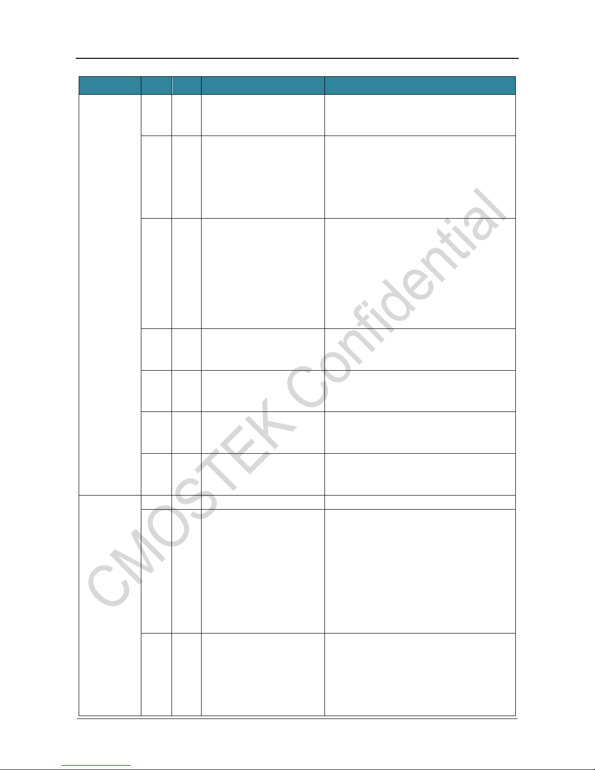
1.2 Duty-Cycle Mode in Rx
4 register control bits are used to control Duty-Cycle mode in Rx. The followings discuss the 5 combinations based on the 4
control bits and the corresponding operating modes.
In the below state transition diagrams, the gray line represents state switching through sending go_* command by MCU. The blue
line represents automatic state switching by chip. It should be noted that during switching from state Ato state B, a blue line and a
gray one cannot co-exist, meaning that, once automatic control by chip is applied, manual control by MCU is not allowed,
otherwise it will disturb the normal operation of chip and may result in chip crash. On the other hand, once manual switching is
applied, automatic switching cannot be enabled.
1.2.1 Fully Manual Control
No Duty-Cycle is applied in fully manual control mode.
Table 4. Fully Manual Control
Control Bit
Value
SLEEP_TIMER_EN
0
RX_DC_EN
0
RX_TIMER_EN
0
RX_EXIT_STATE
0
AN164
Rev 1.0 | 6/21
www.cmostek.com
SLEEP STBY RFS RX
Figure 2. Fully Manual Control of Receiver
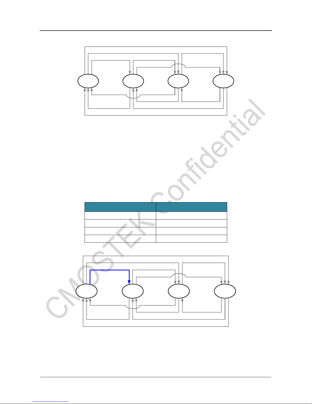
1.2.2 Automatic Wakeup from SLEEP
Only SLEEP timer runs in this mode. After automatic wakeup from SLEEP, the chip switches to STBY waiting for MCU operations.
Based on above information, once a chip enters SLEEP, the MCU cannot send a command to jump out of SLEEP. It can only wait
until the SLEEP timer time out then start operating after detecting the SL_TMO interrupt.
Table 5. Automatic Wakeup from SLEEP
Control Bit
Value
SLEEP_TIMER_EN
1
RX_DC_EN
0
RX_TIMER_EN
0
RX_EXIT_STATE
0
SLEEP_TIMER_EN = 1
SLEEP STBY RFS RX
Figure 3. Automatic Wakeup from SLEEP for Receiver

AN164
Rev 1.0 | 7/21
www.cmostek.com
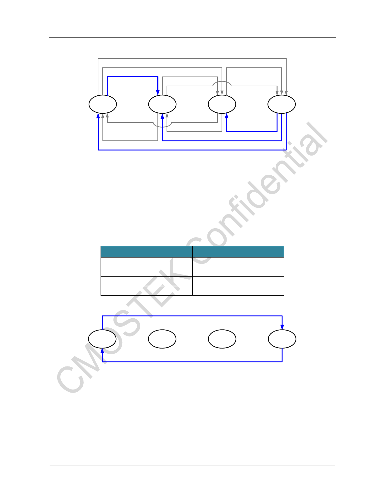
1.2.3 Automatic Wakeup from SLEEP and Enter Rx
Set RX_DC_EN on, then after automatic wakeup from SLEEP, it will not enter STBY, but directly perform PLL calibration and
switch to Rx for receiving instead. In this mode, the RFS state cannot be used and the allowed MCU operations reduce much.
Table 6. Automatic Wakeup from SLEEP and Enter Rx
Control Bit
Value
SLEEP_TIMER_EN
1
RX_DC_EN
1
RX_TIMER_EN
0
RX_EXIT_STATE
0
SLEEP_TIMER_EN = 1, RX_DC_EN = 1
SLEEP STBY RFS RX
Figure 4. Automatic Wakeup from SLEEP and Enter Rx for Receiver
1.2.4 RX Automatic Wakeup from SLEEP and Exit Rx
In this mode, automatic exit function is added based on the automatic wakeup from SLEEP mode. It still needs MCU to
participate in switching from STBY to RFS or RX (no automatic switching to Rx), however, once entering RX, RX TIMER starts
count and then times out, then the chip will switch to the corresponding state based on the configuration of RX_EXIT_STATE. In
general, the STBY state can be used as an intermediate state to allow the MCU to participate in operations such as clearing
interrupts, reading FIFOs.
Table 7. Automatic Wakeup from SLEEP and Exit Rx
Control Bit
Value
SLEEP_TIMER_EN
1
RX_DC_EN
0
RX_TIMER_EN
1
RX_EXIT_STATE
0/1/2
AN164
Rev 1.0 | 8/21
www.cmostek.com
SLEEP STBY RFS RX
RX_TIMER_EN = 1, RX_EXIT_STATE = 0
RX_TIMER_EN = 1, RX_EXIT_STATE = 1
RX_TIMER_EN = 1,
RX_EXIT_STATE = 2
SLEEP_TIMER_EN = 1
Figure 5. Automatic Wakeup from SLEEP and Exit Rx for Receiver
1.2.5 Fully Automatic Receiving
In fully automatic receiving mode, once starting, the chip does not need (and cannot) MCU participating in state switching. The
MCU can get chip operating state through the preset interrupt only then perform required operations. It should be noted that
before entering fully automatic transmission, MCU must accomplish the configuration of the packet format, operating mode of
FIFO, interrupts and IO in the STBY state.
Table 8. Fully Automatic Receiving
Control Bit
Value
SLEEP_TIMER_EN
1
RX_DC_EN
1
RX_TIMER_EN
1
RX_EXIT_STATE
0
SLEEP_TIMER_EN = 1, RX_DC_EN = 1
SLEEP STBY RFS RX
RX_TIMER_EN = 1, RX_EXIT_STATE = 0
Table 9. Fully Automatic Control for Receiver
The limitation of this mode is that it requires MCUs operate fast enough to finish reading FIFO during receiving through interrupt
interaction with chip.
As for cooperation between the MCU and the CMT2219B, users must follow the operating principle, that is, once the automatic
control is applied, do not use the manual control by command to do the same state switching. In addition, it must be noted that if
automatic RX exit function is open, and the target exit state is SLEEP, the interrupt state in control area 2 will be all lost after
exiting to SLEEP. Therefore, when using such a mode, users must pay special consideration to make sure MCU can interact with
chip properly to avoid such condition where MCU fails to get the interrupt. Generally, it is recommended for users to set
RX_EXIT_STATE to 1, that is, chip stays in STBY after exiting RX. At this time, all interrupt states will be retained, the power
consumption will be reduced much, and it allows the MCU to have all required process then switch to SLEEP manually.

AN164
Rev 1.0 | 9/21
www.cmostek.com
1.3 Enter and Exit Duty-Cycle Mode
1.3.1 Enter Duty-Cycle Mode
After chip initialization, in the configuration stage, the related registers are configured then the chip enters Duty-Cycle mode. It
should be noted that the configuration should be done in STBY state and a manual switching to SLEEP should be performed to
ensure the chip runs according to the Duty-Cycle Mode configuration.
1.3.2 Exit Duty-Cycle Mode
In non-automatic Duty-Cycle mode, the system will always stop at a certain state and wait for the MCU to operate. At this time,
the MCU can switch the system back to STBY, then reconfigure a few relevant registers according to the configuration flow
discussed earlier to exit Duty-Cycle mode.
In the fully automatic Duty-Cycle mode, the MCU does not know exact chip operating state, therefore it needs a reliable
mechanism for the MCU to exit the automatic running state and switch back to manual control mode.
Assuming that after the initialization configuration as mentioned above, the CMT2219B enters fully automatic Duty-Cycle mode.
To exit this mode, the following register operations are needed.
1. Set DC_PAUSE to 1. There are several possibilities.
a) If it's currently in RX state, it will enter STBY.
b) If it's currently in SLEEP state, it will wait for the sleep timer time out then return to the STBY.
c) If it's currently in TUNE state, it will go to RX state first, then switch according to the principles discussed above .
2. Regardless of the possibilities, the MCU can scan the CHIP_MODE_STA<3:0> register until it is confirmed the chip enters
STBY.
3. Reconfigure the Duty-Cycle related registers to turn off the fully automatic mode (other registers can be configured as well).
Set DC_PAUSE to 0 after the configuration completes, otherwise the chip cannot enter SLEEP.
4. Send the go_sleep command to make the configuration take effect. At this time, the system will stay in SLEEP and wait for
further operation from MCU.
After setting DC_PAUSE to 1, it waits sleep timer time out before entering STBY. The reason for doing so is to make sure the chip
exits fully automatic mode securely. Otherwise, if the system exits fully automatic mode at any time when receiving the command,
it can hardly ensure reliability. In case a too long sleep time is set and users don't want to wait for such a long time to exit, a
second method is supported as follows.
1. Set CONF_RETAIN to 1 (If it is already set in the initialization configuration, no need to set again). Make sure
SLEEP_BYPASS_EN is set to 0.
2. Send a soft reset or an external reset.
3. Scan the CHIP_MODE_STA<3:0> registers until the chip is in the SLEEP state.
4. Send the go_stby command immediately to switch the chip to STBY mode.
5. Do related configuration then send go_sleep.
This method does not use the DC_PAUSE register, since the MCU surely knows that the chip enters the SLEEP state after
initialization and can send go_stby command. In other words, when the MCU cannot completely determine the chip state, it
should not send go_* commands for manual switching, otherwise, it cannot ensure reliability and possibly causes chip crash.
The first method is used in general while the second one is per special requirements. For both methods, make sure the
CMT2219B already enters fully automatic Duty-Cycle mode, then performs the operations, otherwise operation errors will occur.
AN164
Rev 1.0 | 10/21
www.cmostek.com
2 Super Low Power Receiving Mode
The CMT2219B offers a series of configurations to help users achieving super low power receiving to meet different application
requirements. These configurations take in effect when RX_TIMER_EN is set to 1, that is, the RX timer is active. The core of SLP
receiving is to minimize the RX time when no signal appears and extend it properly when signal appears. As a result, it can
achieve both minimal power consumption and stable receiving.
2.1 SLP Receiving Related Registers
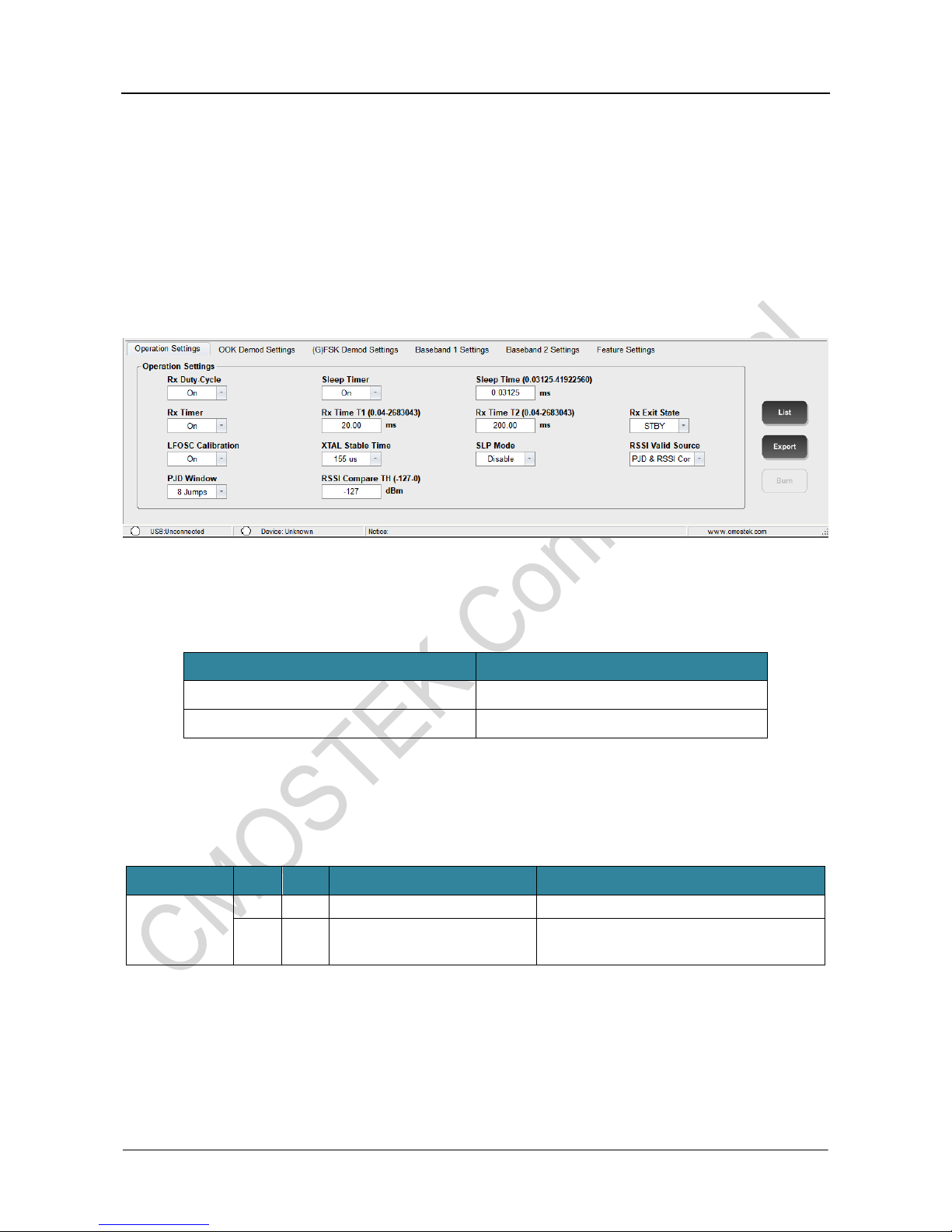
The corresponding RFPDK screen and parameters are shown in the below figure.
Figure 6. RFPDK Screen for SLP
Table 10. SLP Related Parameters
RFPDK Parameter
Register Bits
Fixed to 1
RX_AUTO_EXIT_DIS
SLP Mode
RX_EXTEND_MODE<3:0>
The related registers are listed in the below table.
Table 11. Registers in Configuration Area
Register
Bit
R/W
Flag
Description
CUS_SYS10
(0x15)
5
RW
RX_AUTO_EXIT_DIS
Fixed to 1.
3:0
RW
RX_EXTEND_MODE<3:0>
It defines 14 SLP receiving modes. Refer to the
following chapters for more details.

AN164
Rev 1.0 | 11/21
www.cmostek.com
2.2 Principle of SLP Transmission and Reception
Traditional short-range wireless transceiver systems generally use the following basic solutions to implement low-power
transmission and reception. The CMT2219B is compatible with these solutions. Moreover, it extends 13 more power-saving
solutions based on the traditional ones. Among them, the most fundamental one is discussed below, which can be implemented
through setting RX_EXTEND_MODE<3:0> to 0.
One Packet
IDLE
IDLE
IDLE
Length of Packet x 2 +
Packet Gap < RX Time TX Burst Time > RX Cycle
TX starts transmittion
发射数据:
Missed Received
接收时间:
XTAL,
TUNE
RX Sleep
RX Cycle < TX Burst Time
SLEEP
Receiving Sleeping XTAL stabilizing
and Frequency Tuning
t
t
IDLE
SLEEP SLEEP SLEEP
TX starts transmittion
Received
Figure 7. Fundamental SLP Transmission and Reception Solution
As seen from Figure 7, as long as the below two calculation relationships are satisfied, RX can surely capture the TX data in the
Duty-Cycle receiving mode:
1. A complete RX cycle < the total time of transmitting N packets in bulk by Tx
2. RX time > 2 packets plus 1 packet interval
Among them, a complete RX cycle = RX time + sleep time + crystal startup and settling time + PLL frequency calibration time.
As a summary, in this fundamental low-power solution, subject to the calculation relationship, users need balance between
SLEEP time and the length of transmitted data, other words, users need to choose whether at RX or TX side to make more
energy saving. Moreover, users must set the RX time window large enough to fully capture the data.
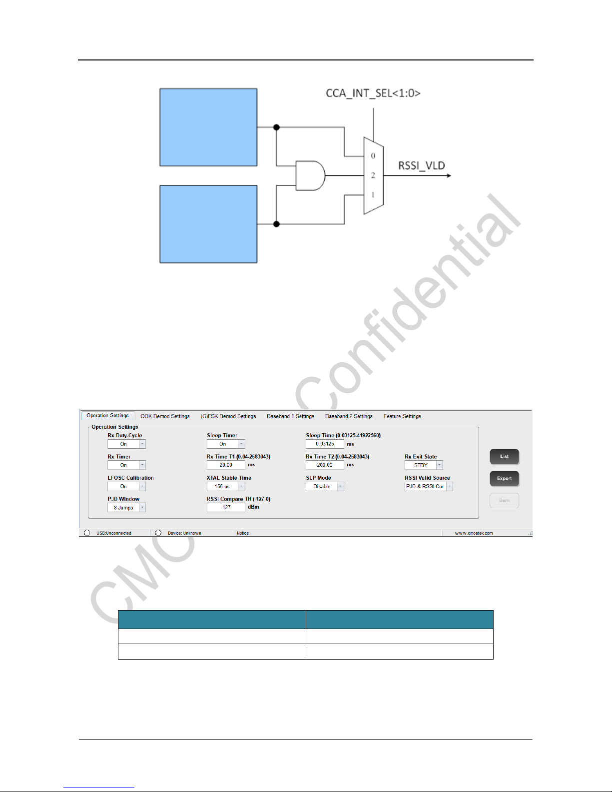
2.3 Channel Listening
As an important supporting mechanism for SLP, channel listening function generates a RSSI_VLD signal by monitoring whether a
valid signal appears (1 indicates the signal appears, 0 indicates noise). The RSSI_VLD signal can not only be used as an
interrupt output to GPIO, but serve as a triggering condition to support SLP implementation.
There are two channel listening mechanisms, PJD (phase jump detector) and RSSI comparison.
Transmitting data
Receiving time
AN164
Rev 1.0 | 12/21
www.cmostek.com
RSSI Comparison
Phase Jump
Detection
Figure 8. Channel Listening Mechanism
It should be noted that PJD can only be used in FSK mode while RSSI comparison can be used in both FSK and OOK modes.
2.3.1 Channel Listening Related Registers
The corresponding RFPDK screen and parameters are shown in the below figure.
Figure 9. RFPDK Screen for Channel Listening
Table 12. Channel Listening Related Parameters
RFPDK Parameters
Register Bits
RSSI Valid Source
CCA_INT_SEL<1:0>
PJD Window
PJD_WIN_SEL<1:0>
The related registers are listed in the below table.
AN164
Rev 1.0 | 13/21
www.cmostek.com
Table 13. Registers in Configuration Area
Register
Bit
R/W
Flag
Description
CUS_SYS11
(0x16)
7
RW
PJD_TH_SEL
The hidden configuration bit of PJD, fixed as 0.
6:5
RW
CCA_INT_SEL<1:0>
Channel listening mode selection.
0: judge signal appearing based on PJD output
1: judge signal appearing based on RSSI comparison
2: meet option 0 and 1 at the same time
3: NA.
Note: in OOK mode, only option 1 can be selected.
CUS_SYS12
(0x17)
7:6
RW
PJD_WIN_SEL<1:0>
This parameter defines how many phase jumps the PJD
needs to detect to determine a signal appearing.
0: 4
1: 6
2: 8
3: 0
2.3.2 RSSI Comparison
The principle of RSSI comparison is that when the RSSI of signal or noise is higher than the thresholds, RSSI_VLD is active,
otherwise it is invalid. The advantage of this method is it is applicable to both FSK and OOK. However the disadvantage is that it
needs debugging and testing in actual application environments to obtain proper thresholds and should try to avoid being
triggered by noise and interference signals. Please refer to the chapter RSSI measurement and comparison for more details. In
short, using RSSI_VLD to support SLP is not an ideal solution yet. Therefore, users can pay more attention on the PJD method
discussed in the following chapter.
2.3.3 Phase Jump Detection (PJD)
As a new technique, PJD identifies signal and noise based on phase jump detection of received signals during FSK
demodulation,. A transit from 0 to 1 (or from 1 to 0) is recognized as a phase jump. Users just need to configure
PJD_WIN_SEL<1:0> to inform JPD that how many phase jumps it needs to detect and judge a PJD.
2
SYM
2
SYM
1
SYM
1
SYM
1
SYM
1
SYM
Figure 10. Received Signal Phase Jump Diagram
As shown in Figure 10, 6 phase jumps appear in the total 8 received symbols, that is, the number of jumps is not equal to the
number of received symbols, however, it is true only when preamble is received. Users need pay attention to this when setting
the related parameters.
How the RSSI_VLD signal supports in implementing super low power (SLP) receiving mode will be discussed in the following
chapters. In general, the more phase jumps appear, the more reliable the judgement is. The less, the faster the judement finishes.
If the receiving time window is small, the number of detections needs to be reduced to adapt the time window setting.
AN164
Rev 1.0 | 14/21
www.cmostek.com
According to the test data, in general, 4 phase jump times can reach a quite reliable detection result, meaning that it will neither
misjudge a noise as a useful signal nor fail to detect a useful signal.
2.4 SLP Receiving Modes
As discussed above, the core of SLP is to control Rx time to achieve this purpose: when there is no useful signal, RX time is very
short and used only to detect whether the useful signal arrives; when a useful signal arrives, RX time is extended to receive data
packets successfully.
Therefore, SLP has further Rx control based on the various manual, semi-automatic, and fully automatic RX Duty-Cycle control
modes described above, other words, all the 14 SLP modes defined by RX_EXTEND_MODE<3:0> aim for RX time control.
Manual or automatic controls other than the RX state control is not relevant to SLP. Users can implement different SLP modes
based on different RX Duty-Cycle modes.
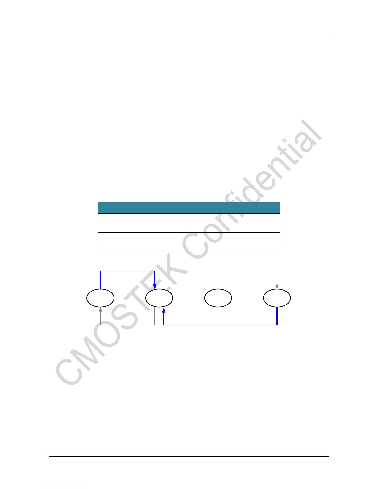
Followings will discuss the 14 SLP modes. Assume that the CMT2219B operates in a RX Duty-Cycle mode as: 1) wakeup from
SLEEP mode automatically 2) exit RX automatically then switch to STBY 3) switch from STBY to SLEEP then switch from STBY
to Rx by MCU.All the 13 SLP models evolve on the this basis.
Table 14. RX Duty-Cycle Mode for SLP
Control Bit
Value
SLEEP_TIMER_EN
1
RX_DC_EN
0
RX_TIMER_EN
1
RX_EXIT_STATE
1
SLEEP STBY RFS RX
RX_TIMER_EN = 1, RX_EXIT_STATE = 1
SLEEP_TIMER_EN = 1
Figure 11. RX Duty-Cycle Mode for SLP
The following 14 SLP modes are based on the above RX Duty-Cycle mode. T1 and T2 in the below table refer to T1 and T2 time
windows of RX, which are set by registers.
AN164
Rev 1.0 | 15/21
www.cmostek.com
Table 15. 14 SLP modes
#
RX Extension Mechanism
RX Extension Condition
0
If it is set as 0, it leaves Rx when T1 timer ends
without Rx extension.
NA
1
In T1 time window, once the condition is detected
as valid, it exits T1 and hands in control to MCU.
RSSI_VLD is valid
2
PREAM_OK is valid
3
RSSI_VLD and PREAM_OK are both valid
4
In T1 time window, once RSSI is detected as valid,
it exits T1 but stays in Rx until RSSI is detected as
invalid then exits Rx.
RSSI_VLD is valid
5
In T1 time window, once the condition is detected
as valid, it switches to T2 then exits Rx when T2
timer ends.
RSSI_VLD is valid
6
PREAM_OK is valid
7
RSSI_VLD and PREAM_OK are both valid
8
PREAM_OK or SYNC_OK is valid
9
PREAM_OK or NODE_OKis valid
10
Any one of PREAM_OK, SYNC_OK or NODE_OK is valid
11
In T1 time window, once RSSI is detected as valid,
it switches to T2. Then in T2 time window, once
SYNC is detected, it exits T2 and hands in control
to MCU, othewise exits Rx when T2 timer ends.
RSSI_VLD is valid
12
PREAM_OK is valid
13
RSSI_VLD and PREAM_OK are both valid
Among the 14 modes discussed above, there are several modes using RSSI_VLD as triggering condition. The CMT2219B
innovatively designs the feature using the RSSI_VLD generated by PJD supporting SLP with remarkable performance. Thus it is
surely a highly recommended feature for users. Option 3 combines RSSI_VLD and PREAM_OK generated by PJD as triggering
conditions, which increases the reliability without much time cost.
When option 3 is used, assuming a transmitter will send a preamble long enough, T1 can be set based on followings.
Reserve 8 symbols for the receiver to perform AFC, set the number of PJD jumps to 6, set the preamble length to 4 or 8 symbols
and increase 6 - 8 symbols time to detect the extension condition, RSSI_VLD& PREAM_OK. Thus T1 time window is a total of 14
- 16 symbols. If the crystal frequency deviation between the transmitting and receiving sides is not large, for example, much
smaller than the configured deviation, the first 8 symbols time for AFC can be reduced based on users' practical measurements.
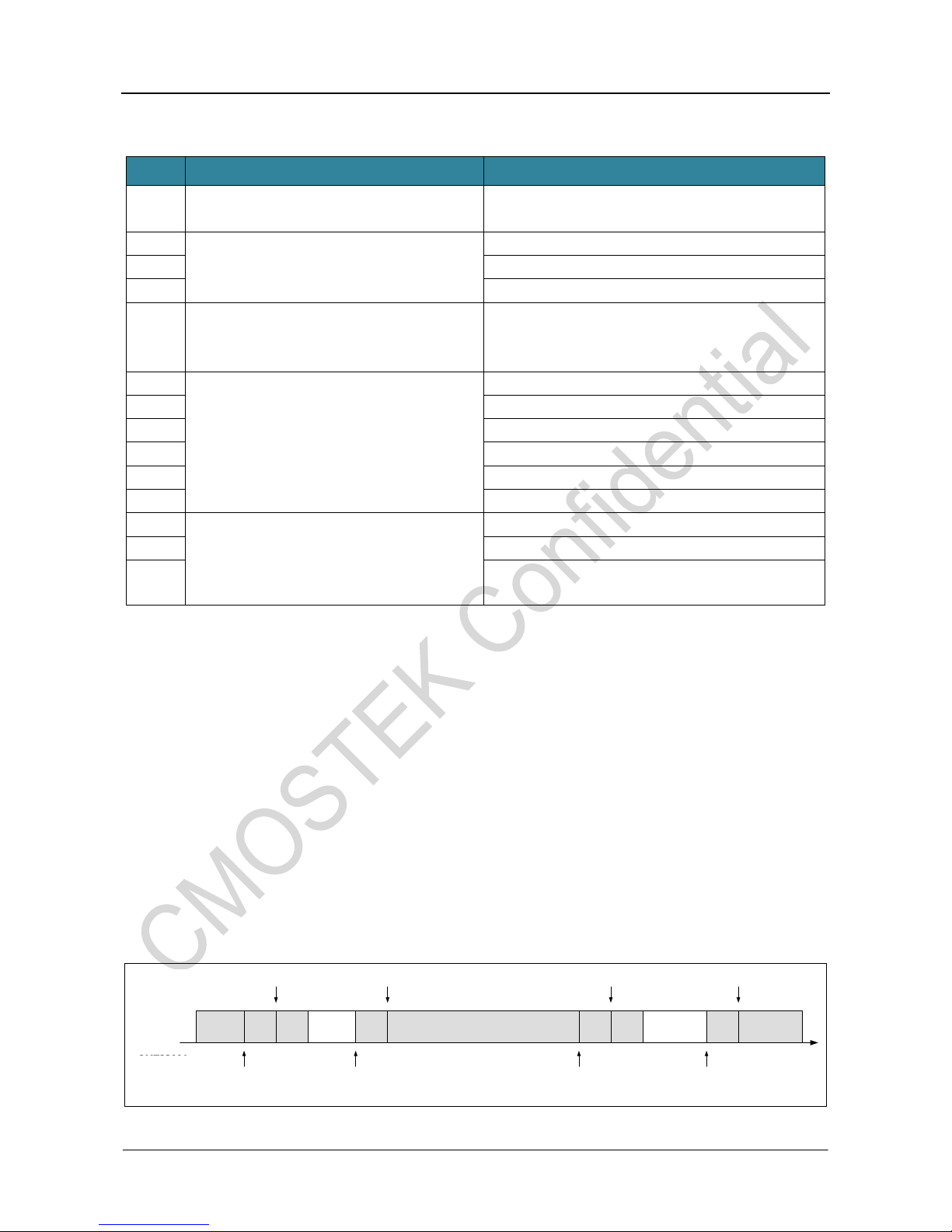
2.4.1 SLP Mode 0
When the mode is set to 0, the receiving time is equal to RX T1 with no extension. As seen from the below diagram, MCU
participates only in sending go_rx and go_sleep commands to switch states while the CMT2219B performs automatic wakeup
from sleep, automatic RX exit and corresponding interrupts generation.
Note that the RX and SLEEP time in the below figure is just for example with no specific meanings.
RX T1
(30 ms)
SLEEP STBY STBY SLEEP (500 ms) RX T1
(50 ms)
STBY STBYCAL CAL SLEEP
go_rx
RX_TMO
go_sleep go_rx go_sleep
CMT2300A
行为
MCU
控制
SL_TMO SL_TMO RX_TMO
Figure 12. SLP Mode 0
MCU
control
CMR2219B
behavior

AN164
Rev 1.0 | 16/21
www.cmostek.com
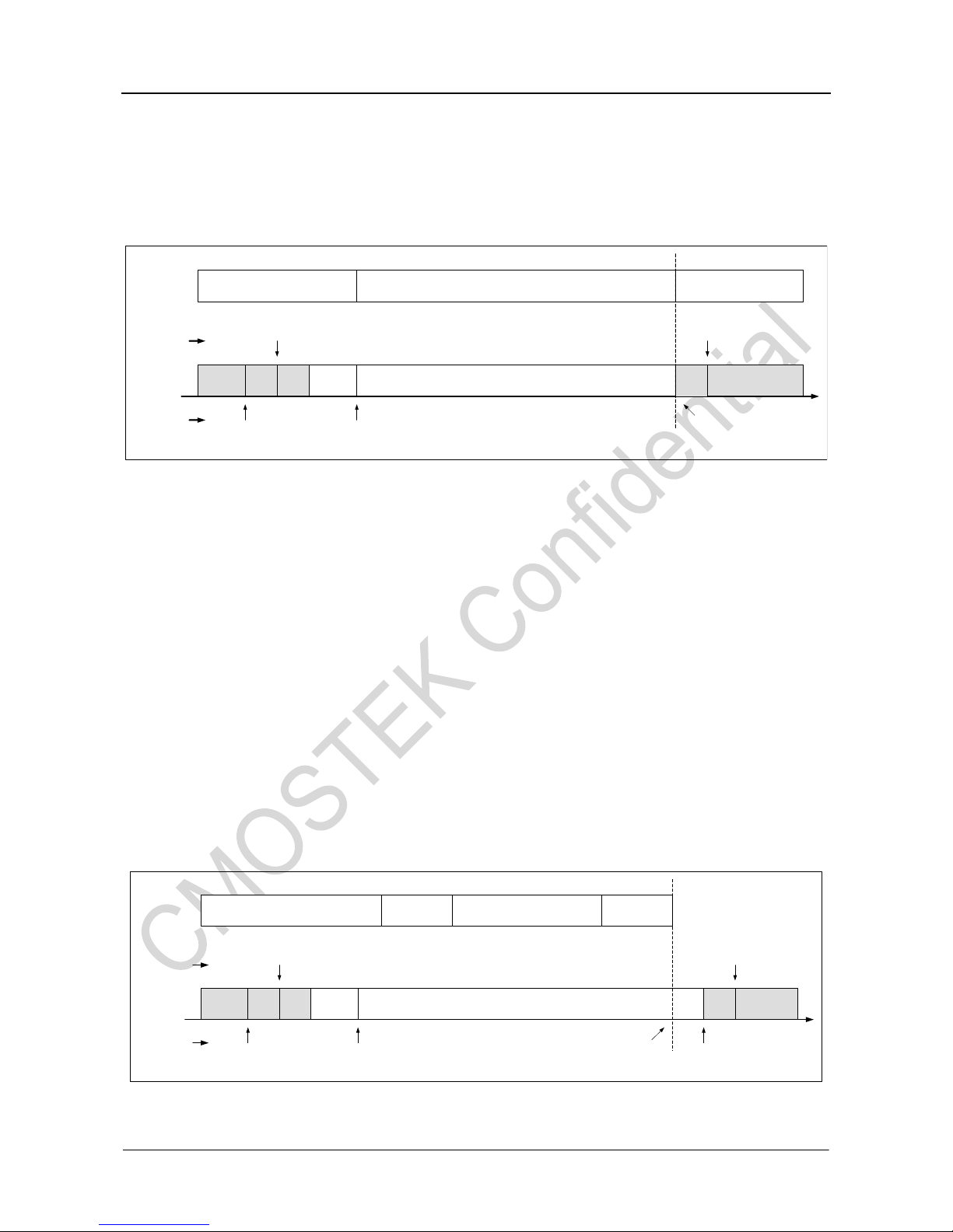
2.4.2 SLP Mode 1 - 3
When the mode is set to 1 - 3, in T1 time window, if the condition is detected as valid, RX T1 stops counting, the chip stays in RX,
exits T1 and hands in control to MCU. Otherwise it exits Rx when T1 timer ends. The 3 different conditions are as follows.
1. The detection condition is RSSI_VLD being valid.
2. The detection condition is PREAM_OK being valid.
3. The detection condition is both RSSI_VLD and PREAM_OK being valid at the same time.
Take condition 2 as an example, the timing diagram for co-working among TX, MCU and RX is shown in the below figure.
RX T1
(10 ms)
SLEEP STBY CAL SLEEP
go_rx
PREAM_OK有效
go_sleep
MCU
操作
Preamble Sync Word Data CRC
RX (等待MCU操作)
PKT_OK有效
TX
数据包
SL_TMO
CMT2300A
行为
Tx packet
MCU control
CMT2219B
behavior PREAM_OK valid
Rx (wait for MCU operation)
PKT_OK valid
Figure 13. SLP Mode 1 - 3
It should be noted that, although the preset time of the RX T1 is 10 ms, it will stop once the detection condition is met, for
example it may stop at 7.5 ms. Then Rx T1 is reset and re-counts when chip entering RX the next time.
The mode 1 - 3 are more suitable for the scenarios below.
In some applications, the TX transmission data varies much, that is, the content, packet length and number of packet are not
fixed. In this case, when the detection condition is met, RX T1 stops and hands in control to MCU, which knows better how long it
should keep in Rx state per specific requirement.
A comparison of the 3 detection conditions is as follows.
Condition 1 is per RSSI_VLD, output result of channel listening. As above mentioned, channel listening along with PJD function
can make fast and reliable judgment on whether a useful signal appears, which has the key advantages of no data format limit,
no need to transmit long preambles, etc. In short, the advantage of option 1 is that it can make sure reliable detection and
judgment even RX T1 time window is set to a small value (for example, 5-8 symbols).
Condition 2 is per PREAM_OK, an interrupt generated by packet, which is a traditional detection condition. Generally a preamble
length of at least 2 bytes is required to ensure reliable detection. It has the advantage of easy-for-understanding. However the
disadvantage is that, to ensure reliable detection it requires that preambles are contained in package, the length of transmitted
preamble of TX must be long enough (covering 2 RX T1 plus 1 SLEEP time), and the RX T1 can cover 2-byte or even longer
preambles.
Condition 3 is both option 1 and 2 being valid at the same time, a more strict condition, which cannot be triggered easily thus with
higher reliability. The RX_PREAM_SIZE of CMT2219B, which can be set to a minimal value of 4 symbols, co-working with
RSSI_VLD signal, will not increase the time of RX T1 and can achieve more reliable detection.
AN164
Rev 1.0 | 17/21
www.cmostek.com
2.4.3 SLP Mode 4
When the mode is set to 4, in T1 time window, once RSSI_VLD is detected as valid, RX T1 stops counting, the chip stays in RX
and then exits Rx automatically until RSSI_VLD is invalid. If no RSSI_VLD is detected in T1, it exits Rx when T1 timer ends.
RX T1
(10 ms)
SLEEP STBY CAL SLEEP
go_rx
RSSI_VLD有效
go_sleep
MCU
操作
噪声 连续发射数据,功率不消失(RSSI一直有效)
RX
RX_TMO
TX
数据包
SL_TMO
CMT2300A
行为
噪声
STBY
Tx packet
MCU control
CMT2219B
behavior
Noise
RSSI_VLD active
NoiseTransmitting data continuously, power keeps active (RSSI keeps active)
Figure 14. SLP Mode 4
2.4.4 SLP Mode 5 - 10
When the mode is set to 5 - 10, in T1 time window, once the condition is detected as valid, it switches to RX T2 then exits Rx
automatically when RX T2 timer ends. Otherwise if the condition is not detected within RX T1, it exits RX when T1 timer ends.
The 6 different conditions are as follows.
5: the detection condition is RSSI_VLD being valid.
6: the detection condition is PREAM_OK being valid.
7: the detection condition is RSSI_VLD and PREAM_OK being valid at the same time.
8: the detection condition is either PREAM_OK or SYNC_OK being valid.
9: the detection condition is either PREAM_OK or NODE_OK being valid.
10: the detection condition is PREAM_OK or SYNC_OK or NODE_OK being valid.
Take condition 6 as an example, the timing diagram for co-working among TX, MCU and RX is shown in the below figure.
RX T1
(10 ms)
SLEEP STBY CAL SLEEP
go_rx go_sleep
Preamble Sync Word Data CRC
RX T2
(100 ms) STBY
RX_TMO
TX
Packet
MCU
Operation
PREAM_OK validSL_TMO PKT_OK valid
CMT2219B
behavior
Figure 15. SLP Mode 5 - 10

AN164
Rev 1.0 | 18/21
www.cmostek.com
User need to set the RX T2 long enough to receive required data entirely.
The mode 5 - 10 are more suitable for the scenarios below.
Compared with mode 1 - 3, mode 5 - 10 differ in the design of RX T2. When switching to RX T2, it will exit Rx automatically when
T2 timer ends with no need for MCU control or MCU effort to take care timeout. Therefore these modes are more suitable for
applications that the transmitted data each time having similar data length, thus it is easy to set proper value to RX T2.
Furthermore, mode 8 - 10 are more practically used in following application cases.
In some cases, to minimize power consumption of TX/RX, the low-power transceiver solution will not meet the calculation
principles described in chapter 2.4. For example, the RX time may be set to a relatively short time resulting in only a proportion of
the detection conditions sent by TX being captured, meaning that 100% capturing is not ensured. By setting anyone within 2 or 3
conditions valid, it will increase the probability of successful capture, however the reliability will decline accordingly. Note that if
user applications are proven working reliably in real applications by using PJD supported RSSI_VLD, it's not necessary to use
option 8 - 10.
Moreover, if there is no NODE ID in package format, option 9 and 10 can be used.
Set the packet format related register NODE_FREE_EN to 1 when there is no NODE ID in package format, meaning that the
NODE_VALUE register is no longer used to define the NODE ID, but to define a code value according to different NODE_SIZE.
When detecting data matching with this code value, a NODE_OK interrupt will be generated, which satisfies condition 9 or 10.
2.4.5 SLP Mode 11 - 13
When the mode is set to 11 - 13, in T1 time window, once the detection condition is detected as valid, it switches to RX T2. Then
in Rx T2, when SYNC_OK is detected, it stops T2 counting, stays in Rx and hands in control to MCU. Otherwise if the condition is
not detected within RX T1, it exits RX when T1 timer ends. The 3 different conditions are as follows.
11:the detection condition is RSSI_VLD being valid.
12:the detection condition is PREAM_OK being valid.
13:the detection condition is both RSSI_VLD and PREAM_OK being valid at the same time.
RX T1
(10 ms)
SLEEP STBY CAL
go_rx
Preamble Sync Word Data CRC
RX ( wait for MCU operation)
RX T2
(30 ms)
PKT_OK
SL_TMO PREAM_OK valid SYNC_OK valid
SLEEP
go_sleep
STBY
go_stby
TX
packet
MCU
control
CMT2219B
Behavior
Figure 16. SLP Mode 11-13

AN164
Rev 1.0 | 19/21
www.cmostek.com
The following scenarios are more suitable to apply modes 11 to 13:
These 3 modes can be used for applications with preamble and sync word contained in data packets. The advantage of these
modes are as follows. When different types of transmission data contained in a channel, the detection of preamble or RSSI is not
enough to indicate desired data reception. Adding fixed sync word as the secondary detection condition will make it reliable
enough. If the secondary detection condition is not satisfied, it exits Rx when RX T2 timer ends to avoid extra power consumption
in case of triggering by fault.

AN164
Rev 1.0 | 20/21
www.cmostek.com
3 Revise History
Table 16. Revise History Records
Version No.
Chapter
Description
Date
1.0
All
Initial version
2017-11-21
Other manuals for CMT2219B
1
Table of contents
Other CMOSTEK Receiver manuals


Popular Receiver manuals by other brands


Hyundai
Hyundai MCR 1 instruction manual

Lectrosonics
Lectrosonics Venue quick start guide

Carrier
Carrier XCT 7 manual

Sony
Sony STR-DA7100ES - Fm Stereo/fm-am Receiver Technical background

Panasonic
Panasonic HDMI SA-XR700 operating instructions

Cambium Networks
Cambium Networks PTP 820 Series installation guide