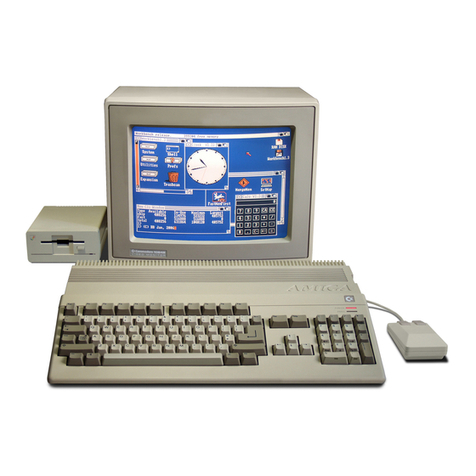
A500 PLUS SERVICE MANUAL
A501 PLUS SPECIFICATIONS
DESCRIPTION
The A501 Plus is amemory expansion board for the Amiga 500 Plus personal computer. It has 1MB of "chip" memory
and interfaces directly to the A500 Plus memory expansion slot. Unlike the A501, the A501 Plus doesn't have aReal
Time Clock (RTC), the A500 Plus has abuilt-in RTC.
The A501 can be used in either the A500 or A500 Plus personal computer, has 512K of memory and includes aReal
Time Clock. The A500 maps the A501 into pseudo-fast memory while the A500 Plus maps it into chip memory. In
addition, when used in an A500 Plus system, the internal (built-in) RTC is selected.
Both the A501 and A501 Plus uses the same printed circuit board (PCB). In the A501 Plus, the RTC and refresh
feature components are not loaded.
MEMORY TYPE
The A501 Plus shall use 256K x 4 120ns DRAMs.
PIN DESCRIPTIONS
PIN
PIN NAME
+5
GND
XDRD (0-15)
XDRA (0-8)
/EXTICK
/XCLKS
/XOE
/XCASL
/XCASU
/XRAS1
/XRAS0
/XWE
NC
XD (0-3)
XA (2-5)
/XCLKRD
/XCLKWR
+12V
NUMBER
1-2, 51-52
3-4, 21-22,
53-54
5-20
23-31
32
33
34
35
36
37,
38
39
40, 56
41-44
45-48
49
50
55
SIGNAL
DIRECTION
I
I/O
I
O
I/O
I
I
I
I
DESCRIPTION
+5Volts
Signal Ground
Memory Data Bus
Memory Address Bus
Active low. When this signal is asserted, it allows the A500 to
detect the presence of an A501. The A501 Plus does not use
this signal.
Active low. When this signal is asserted, the external RTC is
selected. This signal is not used in the A501 Plus.
Active low. When this signal is asserted, data can be read from
the expansion memory.
Active low. This signal strobes the column address into DRAMs
and corresponds to the low byte of the data word.
Active low. This signal strobes the column address into the
DRAMs and corresponds to the high byte of the data word.
Active low. This signal strobes the row address into the DRAMs
and corresponds to the upper 512K of the expansion RAM.
Active low. This signal strobes the row address into the DRAMs
and corresponds to the lower 512K of the expansion RAM.
Active low. When this signal is asserted, data is written into
the expansion memory.
Not connected.
RTC Data bus. These lines are not used in the A501 Plus.
RTC Address Bus. These lines are not used in the A501 Plus.
Active low. When this signal is asserted, data can be read from
the RTC. This signal is not used in the A501 Plus.
Active low. This signal strobes the data and address into the
RTC. This signal is not used in the A501 Plus.
+12 Volts. This is used on the A501 to charge the battery. This
line is not used on the A501 Plus.
1-2
