Dave Embedded Systems Axel ULite User manual

www.dave.eu [email protected]
ARM Cortex A7 MPCore
CPU Module
Lite Line
HARDWARE MANUAL
DAVE E bedded Syste s
AXEL ULite

AXEL ULite Hardware Manual v.1.0.2
<Page intentionally left blank
August, 2019 2/65

AXEL ULite Hardware Manual v.1.0.2
Table of Contents
1 Preface.....................................................................................................................................7
1.1 About this manual.............................................................................................................7
1.2 Copyrights/Trademarks.....................................................................................................7
1.3 Standards..........................................................................................................................7
1.4 Disclaimers.......................................................................................................................7
1.5 Warranty............................................................................................................................7
1.6 Technical Support.............................................................................................................8
1.7 Related documents...........................................................................................................9
1.8 Conventions, Abbreviations, Acronyms............................................................................9
2 Introduction.............................................................................................................................11
2.1 Product Highlights...........................................................................................................12
2.2 Block Diagram.................................................................................................................13
2.3 Feature Summary...........................................................................................................14
3 Design overview.....................................................................................................................16
3.1 NXP i.MX6UL application processor...............................................................................16
3.2 DDR3 memory bank.......................................................................................................18
3.2.1 Reliable Storage Strategy ..................................................................................... 19
3.2.1.1 Write endurance ..............................................................................................20
3.3 NOR flash bank...............................................................................................................21
3.4 NAND flash bank............................................................................................................22
3.5 Memory map...................................................................................................................22
3.6 Power supply unit...........................................................................................................22
3.7 Power consumption........................................................................................................23
3.8 CPU module connectors.................................................................................................23
4 Mechanical specifications......................................................................................................24
4.1 Board Layout...................................................................................................................24
4.2 Connectors......................................................................................................................25
4.3 Mechanical data table.....................................................................................................26
5 Pinout table............................................................................................................................27
5.1 Carrier board mating connector J2.................................................................................27
6 Peripheral interfaces..............................................................................................................35
6.1 Fixed HW peripherals.....................................................................................................36
6.1.1 Ethernet ................................................................................................................. 36
6.1.2 USB ....................................................................................................................... 37
6.1.2.1 USB OTG 1 .....................................................................................................37
6.1.2.2 USB OTG 2 .....................................................................................................37
6.1.3 MMC/SD/SDIO ...................................................................................................... 38
6.1.3.1 MMC/SD/SDIO1 ..............................................................................................38
6.1.4 SPI ......................................................................................................................... 38
6.1.5 ECSPI1 .................................................................................................................. 39
6.1.6 NAND ..................................................................................................................... 39
August, 2019 3/65

AXEL ULite Hardware Manual v.1.0.2
6.2 Variant base peripherals.................................................................................................40
6.2.1 FULL GPIO configuration ...................................................................................... 40
6.3 HMI configuration – use case 1......................................................................................41
6.3.1 LCD controller ........................................................................................................ 41
6.3.2 ECSPI2 .................................................................................................................. 43
6.3.3 I²C2 ........................................................................................................................ 43
6.3.4 KPP ........................................................................................................................ 43
6.3.5 UART1 ................................................................................................................... 44
6.3.6 UART2 ................................................................................................................... 44
6.3.7 UART3 ................................................................................................................... 44
6.3.8 SAI2 ....................................................................................................................... 44
6.4 IoT Gateway – use case 2..............................................................................................45
6.4.1 ENET2 ................................................................................................................... 46
6.4.2 UART1 ................................................................................................................... 46
6.4.3 UART2 – four wires ............................................................................................... 46
6.4.4 UART3 – four wires ............................................................................................... 47
6.4.5 UART4 – for wires ................................................................................................. 47
6.4.6 UART 5 .................................................................................................................. 47
6.4.7 UART 6 .................................................................................................................. 47
6.4.8 UART 7 .................................................................................................................. 48
6.4.9 UART 8 – for wires ................................................................................................ 48
6.4.10 I²C3 ...................................................................................................................... 48
6.4.11 I²C4 ...................................................................................................................... 48
6.4.12 ECSPI2 ................................................................................................................ 48
6.4.13 ECSPI3 ................................................................................................................ 49
6.4.14 MMC/SD/SDIO2 .................................................................................................. 49
6.5 Customized pin muxing configuration.............................................................................50
7 Power, reset and control........................................................................................................51
7.1 Power Supply Unit (PSU) and recommended power-up sequence...............................52
7.1.1 Power-up sequence ............................................................................................... 54
7.2 Reset scheme and control signals..................................................................................55
7.2.1 CPU_PORn ........................................................................................................... 55
7.3 System boot....................................................................................................................56
7.3.1 Boot options ........................................................................................................... 56
7.3.1.1 SPI NOR / SD option .......................................................................................56
7.3.1.2 NAND / SD option ...........................................................................................57
7.4 Clock scheme.................................................................................................................57
7.5 Recovery.........................................................................................................................57
7.5.1 JTAG Recovery ..................................................................................................... 57
7.5.2 USB Recovery ....................................................................................................... 57
7.5.3 SD/MMC Recovery ................................................................................................ 58
7.6 Multiplexing.....................................................................................................................58
8 Operational characteristics....................................................................................................59
August, 2019 4/65

AXEL ULite Hardware Manual v.1.0.2
8.1 PSU input range..............................................................................................................59
8.1.1 PSU input configuration 0,1 ................................................................................... 59
8.1.2 PSU input configuration 2 ...................................................................................... 59
8.1.3 PSU input configuration 3 ...................................................................................... 59
8.2 Power consumption........................................................................................................59
8.2.1 Configuration1 ....................................................................................................... 60
8.3 Heat Dissipation..............................................................................................................60
9 Application Notes...................................................................................................................61
10 RESERVED AREA registration............................................................................................62
Illustration Index
Fig. 1: AXEL ULite.....................................................................................................................11
Fig. 2: AXEL ULite block diagram.............................................................................................13
Fig. 3: Board layout - top view..................................................................................................24
Fig. 4: Board bottom - top view.................................................................................................25
Fig. 5: Simplified block diagram of integrated power supply unit.............................................53
Fig. 6: Simplified block diagram of reset circuitry and voltage monitoring................................55
Fig. 7: Accessing the RESERVED AREA.................................................................................63
Index of Tables
Tab. 1: Related documents.........................................................................................................9
Tab. 2: Abbreviations and acronyms used in this manual...........................................................9
Tab. 3: CPU, Memories, Buses.................................................................................................14
Tab. 4: Peripherals....................................................................................................................14
Tab. 5: Electrical, Mechanical and Environmental Specifications.............................................15
Tab. 6: DDR3 Specifications.....................................................................................................18
Tab. 7: comparison....................................................................................................................20
Tab. 8: comparison....................................................................................................................20
Tab. 9: NOR flash specifications...............................................................................................21
Tab. 10: NAND flash specifications...........................................................................................22
Tab. 11: mechanical data table.................................................................................................26
Tab. 12: pinout table..................................................................................................................27
Tab. 13: J2 odd pins (1 to 203).................................................................................................30
Tab. 14: J2 even pins (2 to 204)................................................................................................34
Tab. 15: Ethernet interface signals............................................................................................36
Tab. 16: USB1 interface signals................................................................................................37
Tab. 17: USB2 interface signals................................................................................................37
Tab. 18: SD1 interface signals..................................................................................................38
Tab. 19: ECSPI1 interface signals............................................................................................39
Tab. 20: SPI NOR / SD option...................................................................................................56
Tab. 21: NAND / SD option.......................................................................................................57
Tab. 22: Application Notes.........................................................................................................61
August, 2019 5/65

AXEL ULite Hardware Manual v.1.0.2
August, 2019 6/65

AXEL ULite Hardware Manual v.1.0.2
1 Preface
1.1 About this anual
This Hardware Manual describes the AXEL ULite CPU module design
and functions.
Precise specifications for the NXP i.MX6UL processor can be found in
the CPU datasheets and/or reference manuals.
1.2 Copyrights/Trade arks
Ethernet® is a registered trademark of XEROX Corporation.
All other products and trademarks mentioned in this manual are property
of their respective owners.
All rights reserved. Specifications may change any time without
notification.
1.3 Standards
DAVE E bedded Syste s is certified to ISO 9001 standards.
1.4 Disclai ers
DAVE E bedded Syste s does not assume any responsibility about
availability, supplying and support regarding all the products mentioned in
this manual that are not strictly part of the AXEL ULite CPU module.
AXEL ULite CPU modules are not designed for use in life support
appliances, devices, or systems where malfunction of these products can
reasonably be expected to result in personal injury.
DAVE E bedded Syste s customers who are using or selling these
products for use in such applications do so at their own risk and agree to
fully indemnify DAVE E bedded Syste s for any damage resulting
from such improper use or sale.
1.5 Warranty
DAVE E bedded Syste s is guaranteed against defects in material
and workmanship for the warranty period from the shipment date. During
the warranty period, DAVE E bedded Syste s will at its discretion
decide to repair or replace defective products. Within the warranty period,
the repair of products is free of charge provided that warranty conditions
are observed.
The warranty does not apply to defects resulting from improper or
inadequate maintenance or handling by the customer, unauthorized
modification or misuse, operation outside of the product’s specifications
or improper installation or maintenance.
August, 2019 7/65

AXEL ULite Hardware Manual v.1.0.2
DAVE E bedded Syste s will not be responsible for any defects or
damages to other products not supplied by DAVE E bedded Syste s
that are caused by a faulty AXEL ULite module.
1.6 Technical Support
We are committed to making our product easy to use and will help
customers use our CPU modules in their systems.
Technical support is delivered through email to our valued customers.
Support requests can be sent to [email protected] .
Software upgrades are available for download in the restricted access
download area of DAVE Embedded Systems web site:
http://www.dave.eu/reserved-area . An account is required to access this
area and is provided to customers who purchase the development kit
(please contact [email protected] for account requests).
Please refer to our Web site at http://www.dave.eu/products/axel-lite for
the latest product documentation, utilities, drivers, Product Change
Notifications, Board Support Packages, Application Notes, mechanical
drawings and additional tools and software.
August, 2019 8/65

AXEL ULite Hardware Manual v.1.0.2
1.7 Related docu ents
Docu ent Location
DAVE Developers Wiki http://wiki.dave.eu/index.php/Main_Page
Tab. 1: Related documents
1.8 Conventions, Abbreviations, Acrony s
Abbreviation Definition
BTN Button
EMAC Ethernet Media Access Controller
GPI General purpose input
GPIO General purpose input and output
GPO General purpose output
PCB Printed circuit board
PMIC Power Manage ent Integrated Circuit
PSU Power supply unit
RTC Real ti e clock
SOC Syste -on-chip
SOM Syste -on- odule
WDT Watchdog
Tab. 2: Abbreviations and acronyms used in this manual
August, 2019 9/65

AXEL ULite Hardware Manual v.1.0.2
Revision History
Version Date Notes
0.0.1 June 2016 First draft (PRELIMINARY)
0.9.0 August 2016 First Release
1.0.0 Septe ber 2016 Release
1.0.1 Dece ber 2018 Minor fixes
1.0.2 August 2019 Minor fixes
August, 2019 10/65

AXEL ULite Hardware Manual v.1.0.2
2 Introduction
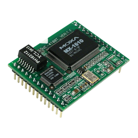
AXEL ULite is the brand new solution made by DAVE Embedded
Systems, based on the recent NXP/Freescale i.MX6UL Ultra Lite
application processor. AXEL ULite defines a new limit in low power
consumption with its ARM Cortex A7 architecture and enables customers
to design a new concept of Embedded IoT devices.
Fig. 1: AXEL ULite
AXEL ULite offers great compromise between computing and power
consumption, thanks to the ARM Cortex-A7 architecture. Additionally, the
use of this processor enables extensive system-level differentiation of
new applications in many industry fields, where power consumption,
connectivity and extremely compact form factor (67,50 mm x around
25,40 mm) are key factors. The advanced security features and the three
different CPU versions available (Base, General Purpose and Security)
offer a wide scenario of applications. Smarter system designs are made
possible, following the trends in functionalities and interfaces of the new,
state-of-the-art embedded products.
August, 2019 11/65

AXEL ULite Hardware Manual v.1.0.2
2.1 Product Highlights
●ULTRA LOW POWER thanks to ARM Cortex A7 MPCore@528 MHz
●pin to pin compatibility with AXEL LITE SOM based on i.MX6
●i.MX6 software full compatibility
●High flexibility with up to 4 different scalable CPU versions (Base, General
Purpose, Security)
●Advanced security thanks to TRNG, Crypto Engine, etc.
●Embedded IoT, connectivity version with "blind CPU"
●Boot from NOR for safe applications
●up to 2 x Ethernet 10/100 Mbps
●Single 3V3 Power Supply with very low power stand by or wide input 3.7-
5.5V
August, 2019 12/65

Fig. 2: AXEL ULite block diagram
AXEL ULite Hardware Manual v.1.0.2
2.2 Block Diagra
August, 2019 13/65

AXEL ULite Hardware Manual v.1.0.2
2.3 Feature Su ary
The following table summarizes the features available with AXEL ULite:
Feature Specifications Options
CPU NXP/Freescale i.MX6 UL
ARM Cortex A7 MPCore @ 528 MHz
Cache L1: 32 Kbyte instruction, 32 Kbyte data
L2: Unified data/instruction, 128 K
SDRAM up to 512 DDR3 -LV, x16 data bus width
NOR SPI NOR 4 -32 MB on request
NAND SLC All sizes, on request
Tab. 3: CPU, Memories, Buses
Feature Specifications Options
LAN Ethernet 10/100 Mbps (PHY on board)
additional MII/RMII interface
Video Input up to 1x CSI port 24 bit parallel
Video
Output
up to 1x RGB Parallel port 24 bit
USB up to 2x 2.0 OTG port (PHY on board)
UARTs up to 8x UART ports
GPIO GPIOs with interrupt capabilities
up to 2x 8ch ADC (12bit)
8x8 Keypad
CAN up to 2x CAN
PC CARD up to 2x SD/MMC
Audio up to 3x I²S / SSI / S / PDIF
Debug JTAG IEEE 1149.1 Test Access Port
Other up to 4x I²C channels
up to 4x SPI channels
up to 8 PWM
Tab. 4: Peripherals
August, 2019 14/65

AXEL ULite Hardware Manual v.1.0.2
Feature Specifications Options
Di ensions 67,50 mm x 25,40 mm
Operating
te perature
range
Commercial (0°C / +70°C) Temperature
Range
Industrial (-40°C / +85°C) Temperature Range
Extended (-40°C / +105°C) Temperature
Range
Weight 6.4 g
Connectors SODIMM 204 pin
Tab. 5: Electrical, Mechanical and Environmental
Specifications
August, 2019 15/65

AXEL ULite Hardware Manual v.1.0.2
3 Design overview
The heart of AXEL ULite module is composed by the following
components:
●NXP i.MX6 UL core SoC application processor
●Power supply unit with 3V3 single rail or wide 3.7-5.5V input
●DDR memory bank
●NOR and NAND flash banks
●204 pin SODIMM connector with interfaces signals. This chapter
shortly describes the main AXEL ULite components.
3.1 NXP i.MX6UL application processor
The i.MX6UL processors feature NXP’s advanced implementation of the
ARM® Cortex®-A7 MPCore, which operates at speeds up to 528MHz.
These SOCs include a deep encryption and security capability, a
complex and flexible boot management and an integrated power
management. As a result that the i.MX6UL devices are able to serve a
wide range of applications including:
●Industrial gateways
●Instrument clusters, and portable medical devices.
●Dataloggers, remote control units
●Human-machine interfaces
●Safety blocks for IoT data manipulation and streaming
August, 2019 16/65

AXEL ULite Hardware Manual v.1.0.2
The i.MX6UL application processor is composed of the following major
functional blocks:
●ARM Cortex-A7 MPCore CPU Processor, featuring:
●128KB unified L2 cache
●NEON MPE co-processor
●External memories interconnect
●Connectivity peripherals, including
●2xRMII - Ethernet 10/100 interfaces
●SD/SDIO/MMC
●Serial buses: USB, UART, I²C, SPI, CAN, …
●On G3 devices:
●Security block, including
●TRNG
●Crypto Engine (AES with DPA, TDES/SHA/RSA)
●Tamper Monitor
●Secure Boot
●SIMV2/EVMSIM X 2
●OTF DRAM Encryption
August, 2019 17/65

AXEL ULite Hardware Manual v.1.0.2
3.2 DDR3 e ory bank
DDR3 SDRAM memory bank is composed by 16-bit width chip.
The following table reports the SDRAM specifications:
Di ension Value
CPU connection Multi-mode DDR controller (MMDC)
Size min 256 MB
Size max 512 GB
Width 16 bit
Speed 400 MHz
Tab. 6: DDR3 Specifications
August, 2019 18/65

AXEL ULite Hardware Manual v.1.0.2
3.2.1 Reliable Storage Strategy
Any embedded product requires to be reliable, robust and economic. This
is the reason why DAVE Embedded Systems introduced the usage of a
good combination of memories that works perfectly in their context and
meet all embedded systems goals. NOR and NAND flash are the key
components of this strategy.
[From Wiki]
NOR and NAND flash differ in two important ways:
●the connections of the individual memory cells are different
●the interface provided for reading and writing the memory is
different (NOR allows random-access for reading, NAND allows
only page access)
These two are linked by the design choices made in the development of
NAND flash. A goal of NAND flash development was to reduce the chip
area required to implement a given capacity of flash memory, and
thereby to reduce cost per bit and increase maximum chip capacity so
that flash memory could compete with magnetic storage devices like hard
disks. [...]
Because of the series connection and removal of wordline contacts, a
large grid of NAND flash memory cells will occupy perhaps only 60% of
the area of equivalent NOR cells.
[..] NAND flash's designers realized that the area of a NAND chip, and
thus the cost, could be further reduced by removing the external address
and data bus circuitry. Instead, external devices could communicate with
NAND flash via sequential-accessed command and data registers, which
would internally retrieve and output the necessary data. This design
choice made random-access of NAND flash memory impossible, but the
goal of NAND flash was to replace mechanical hard disks, not to replace
ROMs.
Attribute NAND NOR
Main Application File Storage Code execution
Storage capacity High Low
Cost per bit Better
Active Power Better
Stability Power Better
Write Speed Good
August, 2019 19/65

AXEL ULite Hardware Manual v.1.0.2
Attribute NAND NOR
Read Speed Good
Tab. 7: comparison
3.2.1.1 Write endurance
The write endurance of SLC floating-gate NOR flash is typically equal to
or greater than that of NAND flash, while MLC NOR and NAND flash
have similar endurance capabilities. Examples of endurance cycle ratings
listed in datasheets for NAND and NOR flash are provided.
Type of flash
e ory
Endurance rating
(Erases per block)
Exa ple(s) of flash
e ory
SLC NAND 100,000 Samsung OneNAND
KFW4G16Q2M
MLC NAND 5,000 to 10,000 for
medium-capacity
applications;
1,000 to 3,000 for high-
capacity applications
Samsung K9G8G08U0M
(Example for medium-
capacity applications)
TLC NAND 1,000 Samsung 840
SLC (floating-gate)
NOR
100,000 to 1,000,000 Numonyx M58BW
(Endurance rating of
100,000 erases per block);
Spansion S29CD016J
(Endurance rating of
1,000,000 erases per
block)
MLC (floating-gate)
NOR
100,000 Numonyx J3 flash
Tab. 8: comparison
However, by applying certain algorithms and design paradigms such as
wear leveling and memory over-provisioning, the endurance of a storage
system can be tuned to serve specific requirements.1
1 https://en.wikipedia.org/wiki/Flash_memory#Distinction_between_NOR_and_NAND_flash
August, 2019 20/65
Table of contents
