decaWave DWM1001 User manual

相关的中文文档请参考 www.decawave.com/china
Overview
The DWM1001 module is based on Decawave's DW1000 Ultra
Wideband (UWB) transceiver IC, which is an IEEE 802.15.4-
2011 UWB implementation. It integrates UWB and Bluetooth®
antenna, all RF circuitry, Nordic Semiconductor nRF52832 and
a motion sensor.
Key Features
•Ranging accuracy to within 10cm.
•UWB Channel 5 printed PCB antenna (6.5 GHz)
•6.8 Mbps data rate
•60 m line-of-sight range typical
•IEEE 802.15.4-2011 UWB compliant
•Nordic Semiconductor nRF52832
•Bluetooth® connectivity
•Bluetooth® chip antenna
•Motion sensor: 3-axis accelerometer
•Current consumption optimised for low power sleep mode: <15μA
•Supply voltage: 2.8 V to 3.6 V
•Size: 19.1 mm x 26.2 mm x 2.6 mm
Key Benefits
•Enables anchors, tags & gateways to quickly get an entire RTLS system up-and-running
•Accelerates product designs for faster Time-to-Market & reduced development costs
•Ready-to-go embedded firmware to minimise software development
•Over-the-air updates
•User API to DWM1001 firmware (available as a library) for user code customisation
•On-board Bluetooth® SMART for connectivity to phones/tablets/PCs
•SPI, UART and Bluetooth® APIs to access DWM1001 firmware from an external device
•Low-power hardware design and software architecture for longer battery life
UWB
Transceiver
Decawave
DW1000
BLE
Microprocessor
Nordic
nRF52832
64 MHz ARM
Cortex M4
SPI M1*
3- Axis Motion
Detector
STM
LIS2DH12TR
BLE Antenna
UART [1:0]
SPI S2* [3:0]
I2C [1:0]
IRQ
UWB Antenna
VCC
2.8 V–3.6 V
DC-DC
Converter
1V8
GPIO
RESET
SWD[1:0]
GPIO
BT_WAKE_UP
GND
READY
4
12
*SPI M1 is nRF52 SPI master 1, SPI S2 is SPI slave 2
High Level Block Diagram

DW1000 Datasheet
Table of Contents
1OVERVIEW ................................................... 5
1.1 UWB TRANSCEIVER DW1000....................... 5
1.2 BLUETOOTH®MICROPROCESSOR NORDIC
NRF52832 ........................................................... 5
1.3 POWER SUPPLY AND POWER MANAGEMENT...... 5
1.4 THREE AXIS MOTION DETECTOR
STMICROELECTRONICS LIS2DH12TR ........................ 5
1.5 SOFTWARE ON BOARD................................... 5
2DWM1001 CALIBRATION ............................. 6
2.1.1 Crystal Oscillator Trim ...................... 6
2.1.2 Transmitter Calibration .................... 6
2.1.3 Antenna Delay Calibration ............... 6
3DWM1001 PIN CONNECTIONS ..................... 7
3.1 PIN NUMBERING.......................................... 7
3.2 PIN DESCRIPTIONS........................................ 7
4ELECTRICAL SPECIFICATIONS ...................... 10
4.1 NOMINAL OPERATING CONDITIONS ............... 10
4.2 DC CHARACTERISTICS.................................. 10
4.3 RECEIVER AC CHARACTERISTICS .................... 10
4.4 RECEIVER SENSITIVITY CHARACTERISTICS ......... 11
4.5 TRANSMITTER AC CHARACTERISTICS .............. 11
4.5.1 Absolute Maximum Ratings ........... 12
5TRANSMIT AND RECEIVE POWER
CONSUMPTION .................................................13
6ANTENNA PERFORMANCE ..........................14
7APPLICATION INFORMATION......................16
7.1APPLICATION BOARD LAYOUT GUIDELINES.......16
8PACKAGE INFORMATION ............................17
8.1 MODULE DRAWINGS................................... 17
8.2 MODULE LAND PATTERN .............................18
8.3 MODULE MARKING INFORMATION ................18
8.4 MODULE SOLDER PROFILE............................ 19
9ORDERING INFORMATION ..........................20
9.1 TAPE AND REEL INFORMATION ......................20
10 GLOSSARY ...............................................21
11 REFERENCES ............................................22
12 DOCUMENT HISTORY ..............................22
13 MAJOR CHANGES ....................................22
14 ABOUT DECAWAVE .................................23
List of Figures
FIGURE 1: DWM1001 PIN DIAGRAM ........................... 7
FIGURE 2: POWER CONSUMPTION DURING TWO WAY
RANGING......................................................... 13
FIGURE 3. ANTENNA RADIATION PATTERN PLANES ......... 14
FIGURE 4: DWM1001 APPLICATION BOARD KEEP-OUT
AREAS ............................................................. 16
FIGURE 5: MODULE PACKAGE SIZE (UNITS:MM)............17
FIGURE 6: DWM1001 MODULE LAND PATTERN (UNITS:
MM)................................................................18
FIGURE 7: DWM1001 MODULE SOLDER PROFILE.........19
FIGURE 8: DWM1001 TAPE AND REEL DIMENSIONS .....20

DWM1001 Datasheet
© Decawave Ltd 2017
Subject to change without notice
Version 1.10
Page 3
List of Tables
TABLE 1: DWM1001 PIN FUNCTIONS ........................... 7
TABLE 2: EXPLANATION OF ABBREVIATIONS..................... 9
TABLE 3: INTERNAL NRF52832 PINS USED AND THEIR
FUNCTION .......................................................... 9
TABLE 4: I2C SLAVE DEVICES ADDRESSI2C....................... 9
TABLE 5: DWM1001 OPERATING CONDITIONS ............ 10
TABLE 6: DWM1001 DC CHARACTERISTICS................. 10
TABLE 7: DWM1001 RECEIVER AC CHARACTERISTICS ... 10
TABLE 8: DWM1001 TYPICAL RECEIVER SENSITIVITY
CHARACTERISTICS .............................................. 11
TABLE 9: DWM1001 TRANSMITTER AC CHARACTERISTICS
...................................................................... 11
TABLE 10: DWM1001 ABSOLUTE MAXIMUM RATINGS. 12
TABLE 11. ANTENNA RADIATION PATTERNS .................. 15
TABLE 12: GLOSSARY OF TERMS.................................. 21
TABLE 13: DOCUMENT HISTORY.................................. 22

DWM1001 Datasheet
© Decawave Ltd 2017
Subject to change without notice
Version 1.10
Page 4
DOCUMENT INFORMATION
Disclaimer
Decawave reserves the right to change product specifications without notice. As far as possible changes to
functionality and specifications will be issued in product specific errata sheets or in new versions of this
document. Customers are advised to check with Decawave for the most recent updates on this product.
The DWM1001 is pre-loaded with firmware, please refer to the "DWM1001 Firmware User Guide" for disclaimer
and license terms.
Copyright © 2017 Decawave Ltd
LIFE SUPPORT POLICY
Decawave products are not authorized for use in safety-critical applications (such as life support) where a
failure of the Decawave product would reasonably be expected to cause severe personal injury or death.
Decawave customers using or selling Decawave products in such a manner do so entirely at their own risk
and agree to fully indemnify Decawave and its representatives against any damages arising out of the use of
Decawave products in such safety-critical applications.
Caution! ESD sensitive device. Precaution should be used when handling the device in order
to prevent permanent damage.
REGULATORY APPROVALS
The DWM1001, as supplied from Decawave, has not been certified for use in any particular geographic region
by the appropriate regulatory body governing radio emissions in that region although it is capable of such
certification depending on the region and the manner in which it is used.
All products developed by the user incorporating the DWM1001 must be approved by the relevant authority
governing radio emissions in any given jurisdiction prior to the marketing or sale of such products in that
jurisdiction and user bears all responsibility for obtaining such approval as needed from the appropriate
authorities.

DWM1001 Datasheet
© Decawave Ltd 2017
Subject to change without notice
Version 1.10
Page 5
1 OVERVIEW
The block diagram on page 1 of this data sheet shows the major sections of the DWM1001. An overview of these
blocks is given below.
1.1 UWB Transceiver DW1000
The module has a DW1000 UWB transceiver mounted on the PCB. The DW1000 uses a 38.4 MHz reference
crystal. The crystal has been trimmed in production to reduce the initial frequency error to approximately 3 ppm,
using the DW1000 IC’s internal on-chip crystal trimming circuit.
Always-On (AON) memory can be used to retain DW1000 configuration data during the lowest power operational
states when the on-chip voltage regulators are disabled. This data is uploaded and downloaded automatically. Use
of DW1000 AON memory is configurable.
The on-chip voltage and temperature monitors allow the host to read the voltage on the VDDAON pin and the
internal die temperature information from the DW1000.
See the DW1000 Datasheet [2] for more detailed information on device functionality, electrical specifications and
typical performance.
1.2 Bluetooth® Microprocessor Nordic nRF52832
The nRF52832 is an ultra-low power 2.4 GHz wireless system on chip (SoC) integrating the nRF52 Series 2.4
GHz transceiver and an ARM Cortex-M4 CPU with 512kB flash memory and 64kB RAM.
See the nRF52832 Datasheet[1] for more detailed information on device functionality, electrical specifications and
typical performance.
1.3 Power Supply and Power management
The power management circuit consists of a switch mode regulator. It is a buck convertor or step down convertor.
The input voltage to the DWM1001 can be in the range 2.8V to 3.6V. Outputs from the convertor provides 1.8V
which is required by the DW1000[2]
1.4 Three Axis Motion Detector STMicroelectronics LIS2DH12TR
The LIS2DH12 is an ultra-low-power high performance three-axis linear accelerometer with digital I2C/SPI serial
interface standard output. The LIS2DH12 has user-selectable full scales of 2g/±4g/8g/16g and is capable of
measuring accelerations with output data rates from 1 Hz to 5.3 kHz. The self-test capability allows the user to
check the functionality of the sensor in the final application. The device may be configured to generate interrupt
signals by detecting two independent inertial wake-up/free-fall events as well as by the position of the device itself.
The LIS2DH12 is guaranteed to operate over an extended temperature range from -40 °C to +85 °C.
See the LIS2DH12TR Datasheet[4] for more detailed information on device functionality, electrical specifications
and typical performance.
1.5 Software on board
The DWM1001 module comes pre-loaded with embedded firmware which provides two-way ranging (TWR) and
real time location system (RTLS) functionality. See the details in the DWM1001 Firmware User Guide [6]. The
module can be configured and controlled via its API, which can be accessed through a number of different
interfaces, allowing flexibility to the product designer. The details of the API are described in the DWM1001
Firmware API Guide [5]. Decawave also provides the module firmware in the form of binary libraries and some
source code. A build environment is provided, so that the user can customise the operation and if required add
their own functions[6].

DWM1001 Datasheet
© Decawave Ltd 2017
Subject to change without notice
Version 1.10
Page 6
2 DWM1001 CALIBRATION
Depending on the end-use applications and the system design, DWM1001 settings may need to be tuned. To
help with this tuning a number of built in functions such as continuous wave TX and continuous packet
transmission can be enabled. See the DW1000 User Manual [3] for further details.
2.1.1 Crystal Oscillator Trim
DWM1001 modules are calibrated at production to minimise initial frequency error to reduce carrier frequency
offset between modules and thus improve receiver sensitivity. The calibration carried out at module production
will trim the initial frequency offset to less than 3 ppm, typically.
2.1.2 Transmitter Calibration
The DWM1001 is calibrated in module production for the on board firmware application.
This is calibrated to meet the power spectral density requirement of less than -41.3 dBm/MHz.
2.1.3 Antenna Delay Calibration
In order to measure range accurately, precise calculation of timestamps is required. To do this the antenna delay
must be known. The DWM1001 allows this delay to be calibrated and provides the facility to compensate for
delays introduced by PCB, external components, antenna and internal DWM1001 delays.
If using the pre-loaded embedded firmware of the DWM1001 module, the Antenna Delay has been pre calibrated
for this configuration. The antenna delay is stored in OTP memory.
If you are creating your own embedded firmware, with a different configuration for the DW1000, then you will
have to calibrate antenna delay. To calibrate the antenna delay, range is measured at a known distance using
two DWM1001 systems. Antenna delay is adjusted until the known distance and reported range agree.
Antenna delay calibration must be carried out as a once off measurement for each DWM1001 design
implementation. If required, for greater accuracy, antenna delay calibration should be carried out on a per
DWM1001 module basis, see DW1000 User Manual [3] for full details. Further details can be found in the
Antenna Delay Application Note [8].
DWM1001 Datasheet
© Decawave Ltd 2017
Subject to change without notice
Version 1.10
Page 7
3 DWM1001 PIN CONNECTIONS
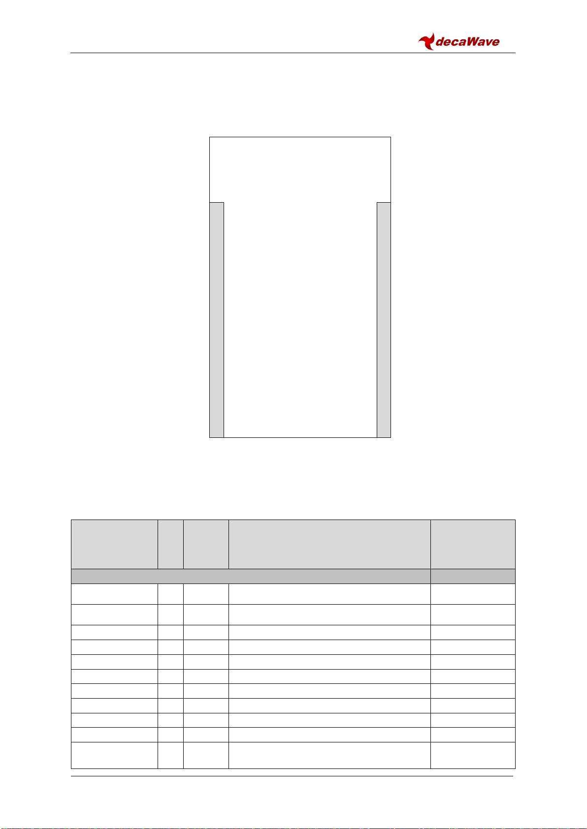
3.1 Pin Numbering
DWM1001 module pin assignments are as follows (viewed from top): -
GND
SWD_CLK
SWD_DIO
GPIO_10
GPIO_9
GPIO_12
GPIO_14
GPIO_22
GPIO_31
GPIO_30
GND
VCC
GPIO_27
I2C_SDA
I2C_SCL
GPIO_23
GPIO_13
34 GND
33 RESETn
32 BT_WAKE_UP
31 GPIO_2
30 GPIO_3
29 SPIS_CSn
28 SPIS_CLK
27 SPIS_MOSI
26 SPIS_MISO
25 GPIO_8
24 GND
23 GPIO_15
22 GPIO_0
21 GPIO_1
20 UART_TX
19 READY
18 UART_RX
1
2
3
4
5
6
7
8
9
10
11
12
13
14
15
16
17
Figure 1: DWM1001 Pin Diagram
3.2 Pin Descriptions
Pin details are given in
Table 1: DWM1001 Pin functions
SIGNAL NAME
PI
N
I/O
(Default
)
DESCRIPTION
REFERENCE (Pin
designation)
Digital Interface
SWD_CLK
2
DI
Serial wire debug clock input for debug and
programming of Nordic Processor
[N] SWDCLK
SWD_DIO
3
DIO
Serial wire debug I/O for debug and
programming of Nordic Processor
[N] SWDIO
GPIO_10
4
DIO
General purpose I/O pin.
[N] P0.10
GPIO_9
5
DIO
General purpose I/O pin.
[N] P0.9
GPIO_12
6
DIO
General purpose I/O pin.
[N] P0.12
GPIO_14
7
DIO
General purpose I/O pin.
[N] P0.14
GPIO_22
8
DIO
General purpose I/O pin.
[N] P0.22
GPIO_31
9
DIO
General purpose I/O pin. ADC function of nRF52
[N] P0.31
GPIO_30
10
DIO
General purpose I/O pin. ADC function of nRF52
[N] P0.30
GPIO_27
13
DIO
General purpose I/O pin.
[N] P0.27
I2C_SDA
(Master)
14
DIO
Master I2C Data Line.
[N] P0.29

DWM1001 Datasheet
© Decawave Ltd 2017
Subject to change without notice
Version 1.10
Page 8
SIGNAL NAME
PI
N
I/O
(Default
)
DESCRIPTION
REFERENCE (Pin
designation)
I2C_SCL
(Master)
15
DO
Master I2C Clock Line
[N] P0.28
GPIO_23
16
DIO
General purpose I/O pin.
[N] P0.23
GPIO_13
17
DIO
General purpose I/O pin.
[N] P0.13
UART_RX
18
DI
UART_RX
[N] P0.11
READY
19
DO
Generated interrupt from the device.
Indicates events such as SPI data ready, or
location data ready.
See the function dwm_int_cfg() in the DWM1001
Firmware API Guide for details[5].
[N] P0.26
UART_TX
20
DO
UART_TX, This is also the ADC function of the
nRF52
[N] P0.05
GPIO_1
21
DIO
General purpose I/O pin of the DW1000.
It may be configured for use as a SFDLED
driving pin that can be used to light a LED when
SFD (Start Frame Delimiter) is found by the
receiver. Refer to the DW1000 User Manual [1]
for details of LED use.
[DW] GPIO1
GPIO_0
22
DIO
General purpose I/O pin of the DW1000.
It may be configured for use as a RXOKLED
driving pin that can be used to light a LED on
reception of a good frame. Refer to the
DW1000 User Manual [1] for details of LED use.
[DW] GPIO0
GPIO_15
23
DIO
General purpose I/O pin.
[N] P0.15
GPIO_8
25
DIO
General purpose I/O pin.
[N] P0.08
SPIS_MISO
26
DI
Configured as a SPI slave this pin is the SPI
data output. Refer to Datasheet for more details
[1].
[N] P0.07
SPIS_MOSI
27
DO
Configured as a SPI slave this pin is the SPI
data input. Refer to Datasheet for more details
[1].
[N] P0.06
SPIS_CLK
28
DI
Configured as a SPI slave this pin is the SPI
clock. This is also the ADC function of the
nRF52
[N] P0.04
SPIS_CSn
29
DI
Configured as a SPI slave this pin is the SPI
chip select. This is an active low enable input.
The high-to-low transition on SPICSn signals the
start of a new SPI transaction. This is also the
ADC function of the nRF52
[N] P0.03
GPIO_3
30
DO
This pin is configured for use as a TXLED
driving pin that can be used to light a LED
during transmit mode. Refer to the DW1000
User Manual [2] for details of LED use.
[DW] GPIO3
GPIO_2
31
DO
This pin is configured for use as a RXLED
driving pin that can be used to light a LED
during receive mode. Refer to the DW1000
User Manual [2] for details of LED use.
[DW] GPIO2
BT_WAKE_UP
32
DI
When this pin is asserted to its active low state
the Bluetooth device will advertise its availability
for 20 seconds by broadcasting advertising
packets. This is also the ADC function of the
nRF52.
[N] P0.02
RESETn
33
DI
Reset pin. Active Low Input.
[N] P0.21
Power Supplies
VCC
12
P
External supply for the module. 2.8V - 3.6V

DWM1001 Datasheet
© Decawave Ltd 2017
Subject to change without notice
Version 1.10
Page 9
SIGNAL NAME
PI
N
I/O
(Default
)
DESCRIPTION
REFERENCE (Pin
designation)
Ground
GND
1,
11,
24,
34
G
Common ground.
Table 2: Explanation of Abbreviations
ABBREVIATION
EXPLANATION
DI
Digital Input
DIO
Digital Input / Output
DO
Digital Output
G
Ground
P
Power Supply
N
nRF52832
DW
DW1000
Note: Any signal with the suffix ‘n’ indicates an active low signal.
Table 3: Internal nRF52832 pins used and their function
nRF52832 Pin
Function
PO.19
DW_IRQ
PO.16
DW_SCK
PO.20
DW_MOSI
PO.18
DW_MISO
PO.17
DW_SPI_CS
PO.24
DW_RST
PO.25
ACC_IRQ
PO.29
I2C_SDA
PO.28
I2C_SCL
DW1000’s GPIOs 5,6 control the DW1000 SPI mode configuration. Within the DWM1001 module, those GPIOs
are unconnected and will be internally pulled down. Consequently, SPI will be set to mode 0. For more details,
please refer to DW1000 data sheet [2].
Table 4: I2C slave devices address I2C
I2C slave device
Address
LIS2DH12
0X19

DWM1001 Datasheet
© Decawave Ltd 2017
Subject to change without notice
Version 1.10
Page 10
4 ELECTRICAL SPECIFICATIONS
The following tables give detailed specifications for the DWM1001 module. Tamb = 25 ˚C for all specifications
given.
4.1 Nominal Operating Conditions
Table 5: DWM1001 Operating Conditions
Parameter
Min.
Typ.
Max.
Units
Condition/Note
Operating temperature
-40
+85
˚C
Supply voltage VCC
2.8
3.3
3.6
V
Normal operation
Voltage on VDDIO for programming OTP
3.7
3.8
3.9
V
Note that for programming the
OTP in the DWM1001 this
supply is connected to the
VDDIO test point which is
underneath the PCB. (See
Figure 6)
4.2 DC Characteristics
Table 6: DWM1001 DC Characteristics
Parameter
Min.
Typ.
Max.
Units
Condition/Note
Supply current in DEEP SLEEP mode
4
µA
All peripherals in lowest
power consumption mode
Achievable where RTC and
accelerometer are disabled
with custom firmware.
Supply current in DEEP SLEEP mode
12
µA
RTC and accelerometer
operational, all other
peripherals in lowest power
consumption mode*
Supply current in IDLE mode
13
mA
MCU and DW1000 awake
TX peak current
111
mA
TX mean current
82
mA
RX peak current
154
mA
RX mean current
134
mA
Current in Bluetooth® discovery mode
6
mA
Digital input voltage high
0.7 x VCC
VCC
V
Digital input voltage low
GND
0.3 x VCC
V
Digital output voltage high
0.7 x VCC
VCC
V
Digital output voltage low
GND
0.3 x VCC
V
* Using a ranging update rate of 1 Hz
4.3 Receiver AC Characteristics
Table 7: DWM1001 Receiver AC Characteristics
Parameter
Min.
Typ.
Max.
Units
Condition/Note
Frequency range
6240
6739.2
MHz
Centre Frequency 6489.6 MHz

DWM1001 Datasheet
© Decawave Ltd 2017
Subject to change without notice
Version 1.10
Page 11
4.4 Receiver Sensitivity Characteristics
Tamb = 25 ˚C, 20 byte payload. These sensitivity figures assume an antenna gain of 0 dBi and should be modified
by the antenna characteristics, depending on the orientation of the DWM1001.
Table 8: DWM1001 Typical Receiver Sensitivity Characteristics
Packet
Error
Rate
Data Rate
Receiver
Sensitivity
Units
Condition/Note
1%
6.8 Mbps
-98*(-92)
dBm/500 MHz
Preamble 128
Carrier
frequency
offset
±10 ppm
All measurements
performed on
Channel 5, PRF 64
MHz
10%
6.8 Mbps
-99*(-93)
dBm/500 MHz
Preamble 128
*equivalent sensitivity with Smart TX Power enabled. This is enabled in the onboard firmware.
4.5 Transmitter AC Characteristics
Table 9: DWM1001 Transmitter AC Characteristics
Parameter
Min.
Typ.
Max.
Units
Condition/Note
Frequency range
6240
6739.2
MHz
Output power spectral density
-41.3*
dBm/MHz
See DW1000 Datasheet [1]
Output Channel Power
-17
dBm/500MHz
Output power variation with
temperature*
-1
+1
dB
Using on board
compensation.
* If using the pre-loaded embedded firmware of the DWM1001 module, otherwise see the DW1000 datasheet

DWM1001 Datasheet
© Decawave Ltd 2017
Subject to change without notice
Version 1.10
Page 12
4.5.1 Absolute Maximum Ratings
Table 10: DWM1001 Absolute Maximum Ratings
Parameter
Min.
Max.
Units
Supply voltage
2.8
3.9
V
Receiver power
0
dBm
Temperature - Storage temperature
-40
+85
˚C
Temperature –Operating temperature
-40
+85
˚C
ESD (Human Body Model)
2000
V
DWM1001 pins other than VCC, VDDIO and GND
3.6
Note that 3.6 V is
the max voltage
that may be
applied to these
pins
Stresses beyond those listed in this table may cause permanent damage to the device. This is a stress rating
only; functional operation of the device at these or any other conditions beyond those indicated in the operating
conditions of the specification is not implied. Exposure to the absolute maximum rating conditions for extended
periods may affect device reliability.

DWM1001 Datasheet
© Decawave Ltd 2017
Subject to change without notice
Version 1.10
Page 13
5 TRANSMIT AND RECEIVE POWER CONSUMPTION
The following Figures give power profiles for the DWM1001 on a DWM1001-DEV PCB when used for Two Way
Ranging, see Figure 2. Peak values are given.
Figure 2 shows an example of the power consumption of a DWM1001 tag running the factory loaded firmware.
The tag is in low-power mode, and two-way ranging with 3 anchors. The deep-sleep current occurs while the tag
is sleeping with only the RTC and accelerometer active.
Once awake, the tag transmits at its allocated time in the TDMA-slotting, and awaits the anchors responses. This
can be observed as 1 transmission followed by 3 receives, repeated once. After this is completed, the tag spends
some time computing its location, before returning to sleep. The total time awake is dependent on the number of
anchors within range of the tag. For more details on the system operation, see the DWM1001 System Overview
document[9].
Figure 2: power consumption during Two Way Ranging
DWM1001 Datasheet
© Decawave Ltd 2017
Subject to change without notice
Version 1.10
Page 14
6 ANTENNA PERFORMANCE
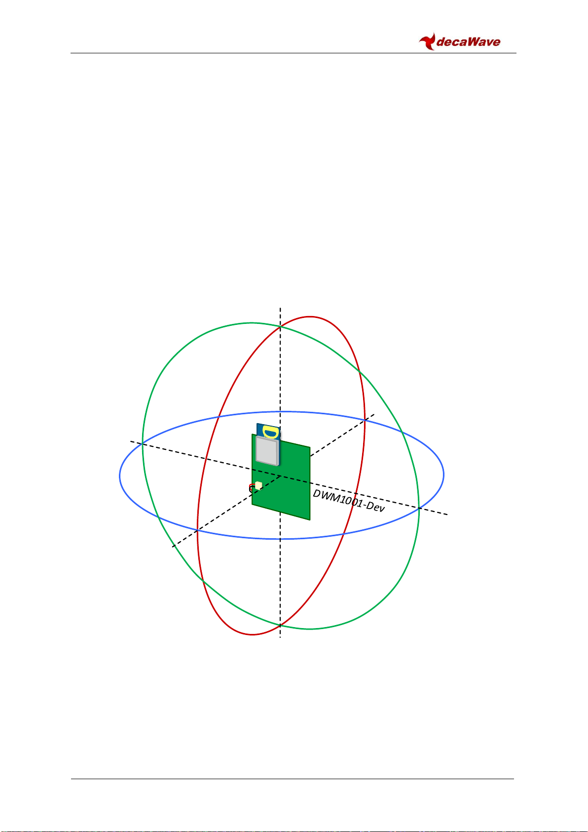
This section details antenna radiation patterns for the DWM1001-Dev board. Figure 3 presents a view of the
measurement planes considered in this document.
Table 11 shows antenna radiation patterns for the DWM1001 module mounted on the DWM1001-Dev board.
Three planes in the spherical space about the centre of the board are measured, with theta and phi plots
representing perpendicular polarisations.
The DWM1001 antenna is vertically polarised, meaning that the module is intended to be positioned vertically
upright when used in an RTLS system. An omnidirectional radiation pattern is seen in the XZ plane when
observed by another antenna which is also vertically polarised. This is shown in the XZ plane antenna patterns,
where the vertically polarised plot, phi, has a circular, or omnidirectional shape.
If the antennas are oriented perpendicular relative to each other, then the polarisation changes. In this case, the
horizontally polarised pattern, theta, applies and there are nulls at certain angles which can limit range and
introduce location inaccuracy.
Figure 3. Antenna Radiation Pattern Planes
x
z
y

DWM1001 Datasheet
© Decawave Ltd 2017
Subject to change without notice
Version 1.10
Page 15
-30
-25
-20
-15
-10
-5
0
5
0816 24 32
40
48
56
64
72
80
88
96
104
112
120
128
136
144
152
160
168
176184
192
200
208
216
224
232
240
248
256
264
272
280
288
296
304
312
320
328 336 344 352
Table 11. Antenna Radiation Patterns
Planes:
Antenna Gain (dBi) vs. Angle (°)
-30
-25
-20
-15
-10
-5
0
5
0816 24 32
40
48
56
64
72
80
88
96
104
112
120
128
136
144
152
160
168
176184
192
200
208
216
224
232
240
248
256
264
272
280
288
296
304
312
320
328 336 344 352
0°
90°
270°
180°
Theta
Phi
XZ Plane:
XY Plane:
YZ Plane:
180°
0°
90°
270°
Theta
Phi
270°
180°
0°
90°
Theta
Phi
-30
-25
-20
-15
-10
-5
0
5
0816 24 32
40
48
56
64
72
80
88
96
104
112
120
128
136
144
152
160
168
176184
192
200
208
216
224
232
240
248
256
264
272
280
288
296
304
312
320
328 336 344 352

DWM1001 Datasheet
© Decawave Ltd 2017
Subject to change without notice
Version 1.10
Page 16
7 APPLICATION INFORMATION
7.1 Application Board Layout Guidelines
When designing the PCB onto which the DWM1001 will be soldered, the proximity of the DWM1001 on-board
antenna to metal and other non-RF transparent materials needs to considered carefully. Two suggested
placement schemes are shown below.
For best RF performance, ground copper should be flooded in all areas of the application board, except
in the areas marked “Keep-Out Area”, where there should be no metal either side, above or below (e.g.
do not place battery under antenna).
The two placement schemes in Figure 4 show an application board with no metallic material in the keep-out
area. The diagram on the right is an application board with the antenna projecting off of the board so that the
keep out area is in free-space. The diagram on the left shows an application board which does not have the
module in free space but has the pcb copper removed on either side (and behind) the module antenna.
(Note: the rectangular area above the shield on the module is the antenna area)
It is also important to note that the ground plane on the application board affects the DWM1001 antenna radiation
pattern. There must be a minimum spacing of 10 mm (d) without metal either side of the module antenna.
Application Board
dd
Application Board
d d
Keep-Out
Area Keep-Out
Area
Figure 4: DWM1001 Application Board Keep-Out Areas

DWM1001 Datasheet
© Decawave Ltd 2017
Subject to change without notice
Version 1.10
Page 17
8 PACKAGE INFORMATION
8.1 Module Drawings
All measurements are given in millimetres.
Figure 5: Module Package Size (units: mm)

DWM1001 Datasheet
© Decawave Ltd 2017
Subject to change without notice
Version 1.10
Page 18
8.2 Module Land Pattern
The diagram below shows the DWM1001 module land pattern.
Figure 6: DWM1001 Module Land Pattern (units: mm)
8.3 Module Marking Information
Each module has a label on the shield with a serial number in the following format:
YY WW 0 SSSSS
Where:
YY indicates the year
WW indicates the week of the year
0 indicates the DWM1001 module
SSSSS indicates the module manufacturing number

DWM1001 Datasheet
© Decawave Ltd 2017
Subject to change without notice
Version 1.10
Page 19
8.4 Module Solder Profile
Figure 7: DWM1001 Module Solder Profile

DWM1001 Datasheet
© Decawave Ltd 2017
Subject to change without notice
Version 1.10
Page 20
9 ORDERING INFORMATION
9.1 Tape and Reel Information
Figure 8: DWM1001 Tape and Reel Dimensions
Table of contents
Popular Control Unit manuals by other brands

Datex-Ohmeda
Datex-Ohmeda B-CPU5 Technical reference manual
Ring Engineering
Ring Engineering AM-1b user manual

FedEx
FedEx SenseAware M4 user guide

Anritsu
Anritsu MT1000A Network Master Pro Operation manual
Texas Instruments
Texas Instruments DS160PR412-421EVM user guide

Opentrons
Opentrons GEN1 instruction manual
weed instrument
weed instrument EOTec 2000 installation instructions

DeZurik
DeZurik APCO CVS-250 instruction manual
Siemens
Siemens SIMOTION Function manual

SolarEdge
SolarEdge ZigBee Plug-in installation guide

Bardiani Valvole
Bardiani Valvole MIXPROOF B915PMO Instruction, use and maintenance manual
Controls
Controls XCAN-AC product manual

