FATTENTION DWARNUNG
WAARSCHUWING
AVVERTIMENTO
WARNING
Safety regulations require that the set be restored to its original condition
and that parts which are identical with those specified be used.
Veiligheidsbepalingen vereisen, dat het apparaat in zijn oorspronkelijke
toestand wordt terug gebracht en dat onderdelen, identiek aan de
gespecifieerde worden toegepast.
Bei jeder Reparatur sind die geltenden Sicherheitsvorschriften zu beachten.
Der Originalzustand des Gerats darf nicht verandert werden.
Fur Reparaturen sind Original-Ersatzteile zu verwenden.
Le norme di sicurezza esigono che l’apparecchio venga rimesso nelle
condizioni originali e che siano utilizzati pezzi di ricambiago idetici a quelli
specificati.
Les normes de sécurité exigent que l’appareil soit remis a l’état d’origine et
que soient utilisées les pièces de rechange identiques à celles spécifiées.
“Pour votre sécurité, ces documents
doivent être utilisés par des
spécialistes agrées, seuls habilités à
réparer votre appareil en panne.”
GB NL
I
D
I
F
GB
NL
All ICs and many other semi-conductors are
susceptible to electrostatic discharges (ESD).
Careless handling during repair can reduce life
drastically.
When repairing, make sure that you are connected
with the same potential as the mass of the set via a
wrist wrap with resistance.
Keep components and tools also at this potential.
Tous les IC et beaucoup d’autres semiconducteurs
sont sensibles aux décharges statiques (ESD).
Leur longévité pourrait être considérablement
écourtée par le fait qu’aucune précaution n’est prise
a leur manipulation.
Lors de réparations, s’assurer de bien être relié au
même potentiel que la masse de l’appareil et enfiler
le bracelet serti d’une résistance de sécurité.
Veiller a ce que les composants ainsi que les outils
que l’on utilise soient également a ce potentiel.
Alle IC und viele andere Halbleiter sind
empfindlich gegen elektrostatische
Entladungen (ESD).
Unsorgfältige Behandlung bei der Reparatur
kann die Lebensdauer drastisch vermindern.
Sorgen sie dafür, das Sie im Reparaturfall
dem Massepotential des Gerätes verbunden
sind.
Halten Sie Bauteile und Hilfsmittel ebenfalls
über ein Pulsarmband mit Widerstand mit auf
diesem Potential.
Alle IC’s en vele andere halfgeleiders zijn gevoelig
voor elektrostatische ontladingen (ESD).
Onzorgvuldig behandelen tijdens reparatie kan de
levensduur drastisch doen verminderen.
Zorg ervoor dat u tijdens reparatie via een polsband
met weerstand verbonden bent met apparaat.
Houd componenten en hulpmiddelen ook op
ditzelfde potentiaal.
Tutti IC e parecchi semi-conduttori sono sensibili
alle scariche statiche (ESD).
La loro longevita potrebbe essere fortemente ridatta
in caso di non osservazione della piu grande
cauzione alla loro manipolazione.
Durante le riparazioni occorre quindi essere
collegato allo stesso potenziale che quello della
massa dell’apparecchio tramite un braccialetto a
resistenza.
Assicurarsi che i componenti e anche gli utensili
con quali si lavora siano anche a questo potenziale.
LASER SAFETY
CAUTION VISIBLE AND INVISIBLE LASER RADIATION WHEN OPEN AVOID EXPOSURE TO BEAM
ADVARSEL SYNLIG OG USYNLIG LASERSTRÅLING VED ÅBNING UNDGÅ UDS
Æ
TTELSE FOR STRÅLING
ADVARSEL SYNLIG OG USYNLIG LASERSTRÅLING NÅR DEKSEL Å PNES UNNGÅ EKSPONERING FOR STRÅLEN
VARNING SYNLIG OCH OSYNLIG LASERSTRÅLNING NÄR DENNA DEL ÄR ÖPPNAD BETRAKTA EJ STRÅLEN
VARO! AVATT AESSA OLET ALTTIINA NÄKYVÄLLE JA NÄKYMÄTTÖMÄLLE LASER SÄTEILYLLE. ÄLÄ KATSO SÄTEESEEN
VORSICHT SICHTBARE UND UNSICHTBARE LASERSTRAHLUNG WENN ABDECKUNG GEÖFFNET NICHT DEM STRAHL AUSSETSEN
DANGER VISIBLE AND INVISIBLE LASER RADIATION WHEN OPEN AVOID DIRECT EXPOSURE TO BEAM
ATTENTION RAYONNEMENT LASER VISIBLE ET INVISIBLE EN CAS D'OUVERTURE EXPOSITION DANGEREUSE AU FAISCEAU
USE OF CONTROLS OR ADJUSTMENTS OR PERFORMANCE
OF PROCEDURE OTHER THAN THOSE SPECIFIED HEREIN
MAY RESULT IN HAZARDOUS RADIATION EXPOSURE.
AVOID DIRECT EXPOSURE TO BEAM
WARNING
The use of optical instruments with this product will
increase eye hazard.
Repair handling should take place as much as possible with
a disc loaded inside the player
WARNING LOCATION: INSIDE ON LASER COVERSHIELD
This unit employs a laser. Only a qualified service person should
remove the cover or attempt to service this device, due to
possible eye injury.
100301DM
WARNING AND LASER SAFETY INSTRUCTIONS
WARNING:
Parts indicated by the z mark have critical characteristics. Use ONLY replacement parts recommended
by the manufacturer.
CAUTION:
Before returning the set to the customer, be sure to carry out either (1) a leakage current check or (2)
a line to chassis resistance check. If the leakage current exceeds 0.5 milliamps, or if the resistance from
chassis to either side of the power cord is less than 460 kohms, the set is defective.
WARNING:
DO NOT return the set to the customer unless the problem is identied and remedied.
NOTICE:
(1) ALL RESISTANCE VALUES IN OHM. k=1,000 OHM / M=1,000,000 OHM
(2) ALL CAPACITANCE VALUES ARE EXPRESSED IN MICRO FARAD, UNLESS OTHERWISE INDICATED. P
INDICATES MICRO-MICRO FARAD. N INDICATES NANO FARAD.
(3) EACH VOLTAGE AND CURRENT ARE MEASURED AT NO SIGNAL INPUT CONDITION.
(4) CIRCUIT AND PARTS ARE SUBJECT TO CHANGE WITHOUT PRIOR NOTICE.
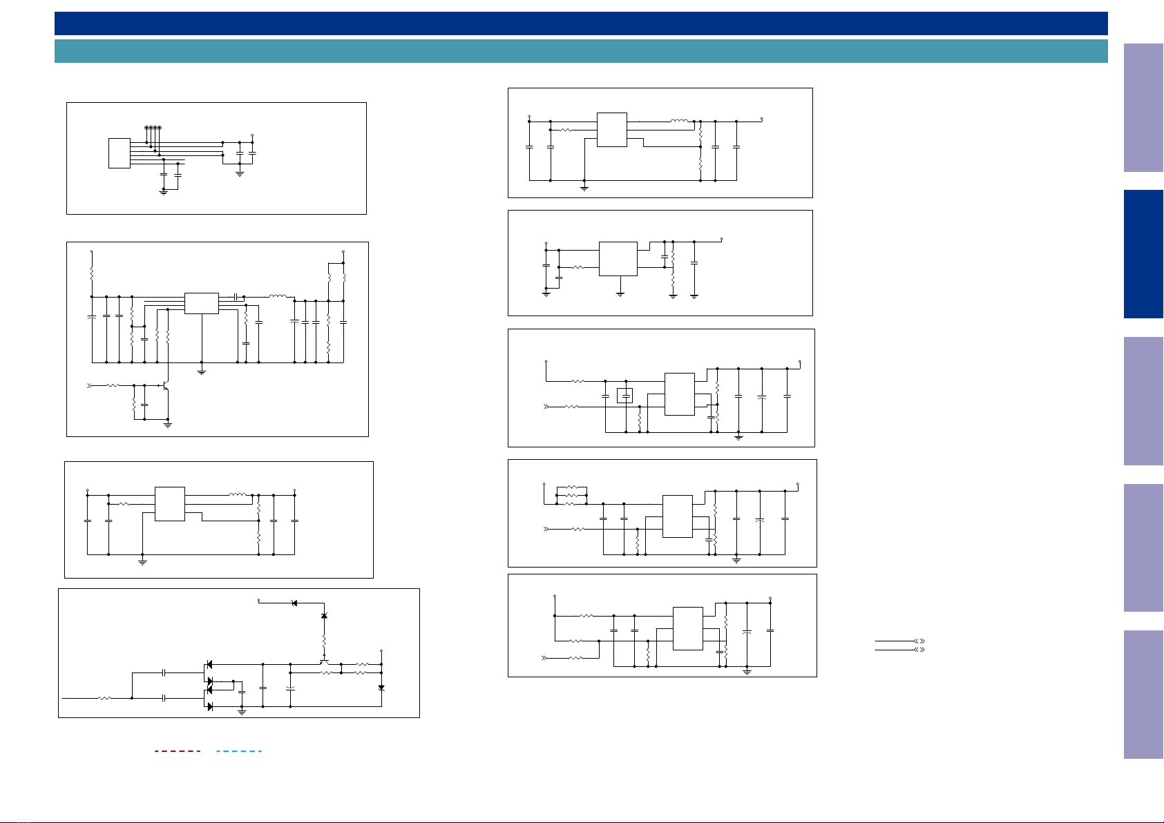
Electrostatic breakdown of the semi-conductors or optical pickup may occur due to a potential differ-
ence caused by electrostatic charge during unpacking or repair work.
1. Ground for Human Body
Be sure to wear a grounding band (1 M ohm) that is properly grounded to remove any static electricity
that may be charged on the body.
2. Ground for Workbench
Be sure to place a conductive sheet or copper plate with proper grounding (1 M ohm) on the work-
bench or other surface, where the semi-conductors are to be placed. Because the static electricity
charge on clothing will not escape through the body grounding band, be careful to avoid contacting
semi-conductors with your clothing
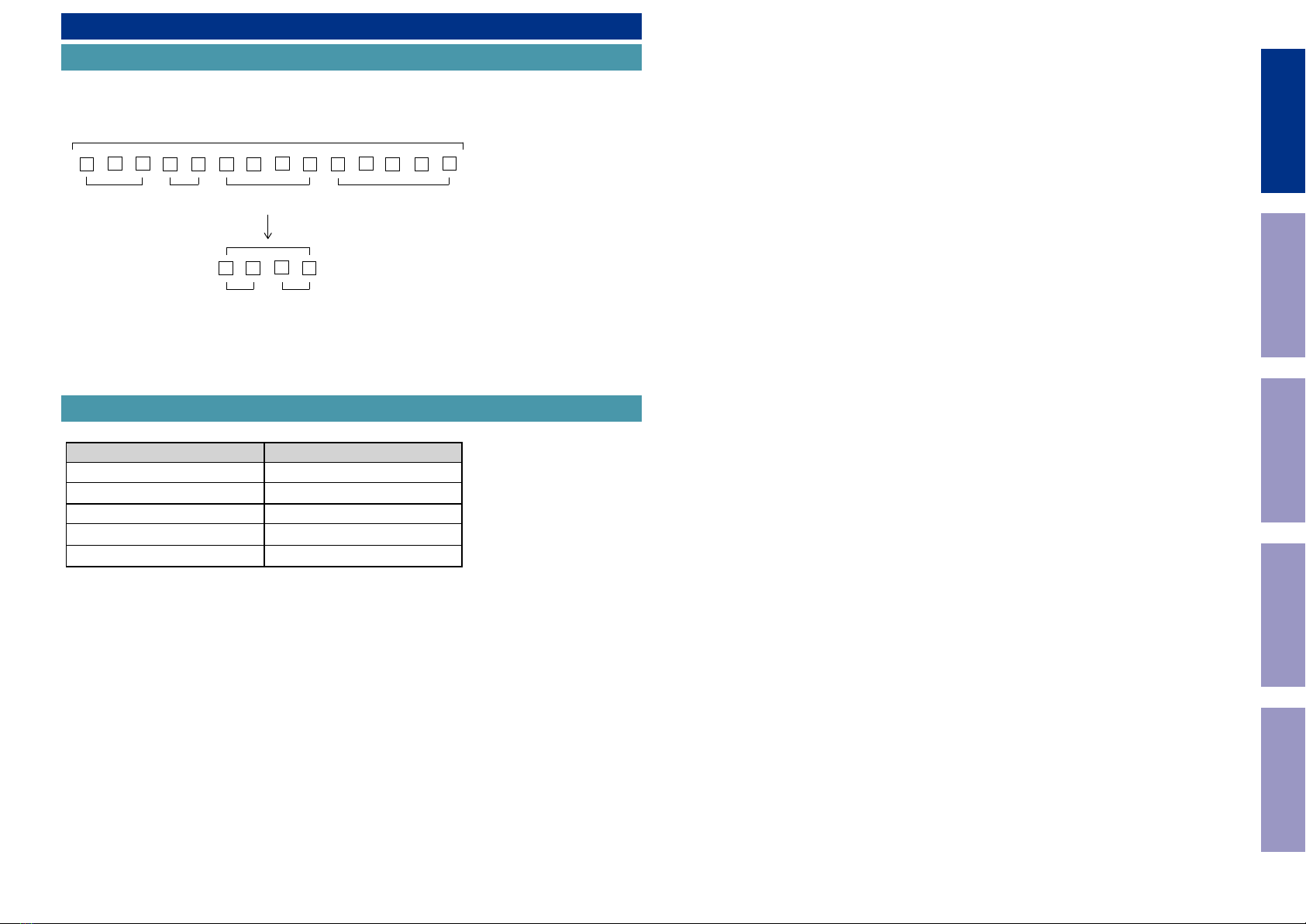
<Incorrect>
CBA
Grounding Band
Conductive Sheet or
Copper Plate
1MΩ
1MΩ
<Correct>
CBA
NOTE FOR SCHEMATIC DIAGRAM
HANDLING THE SEMICONDUCTOR AND OPTICS
Before Servicing
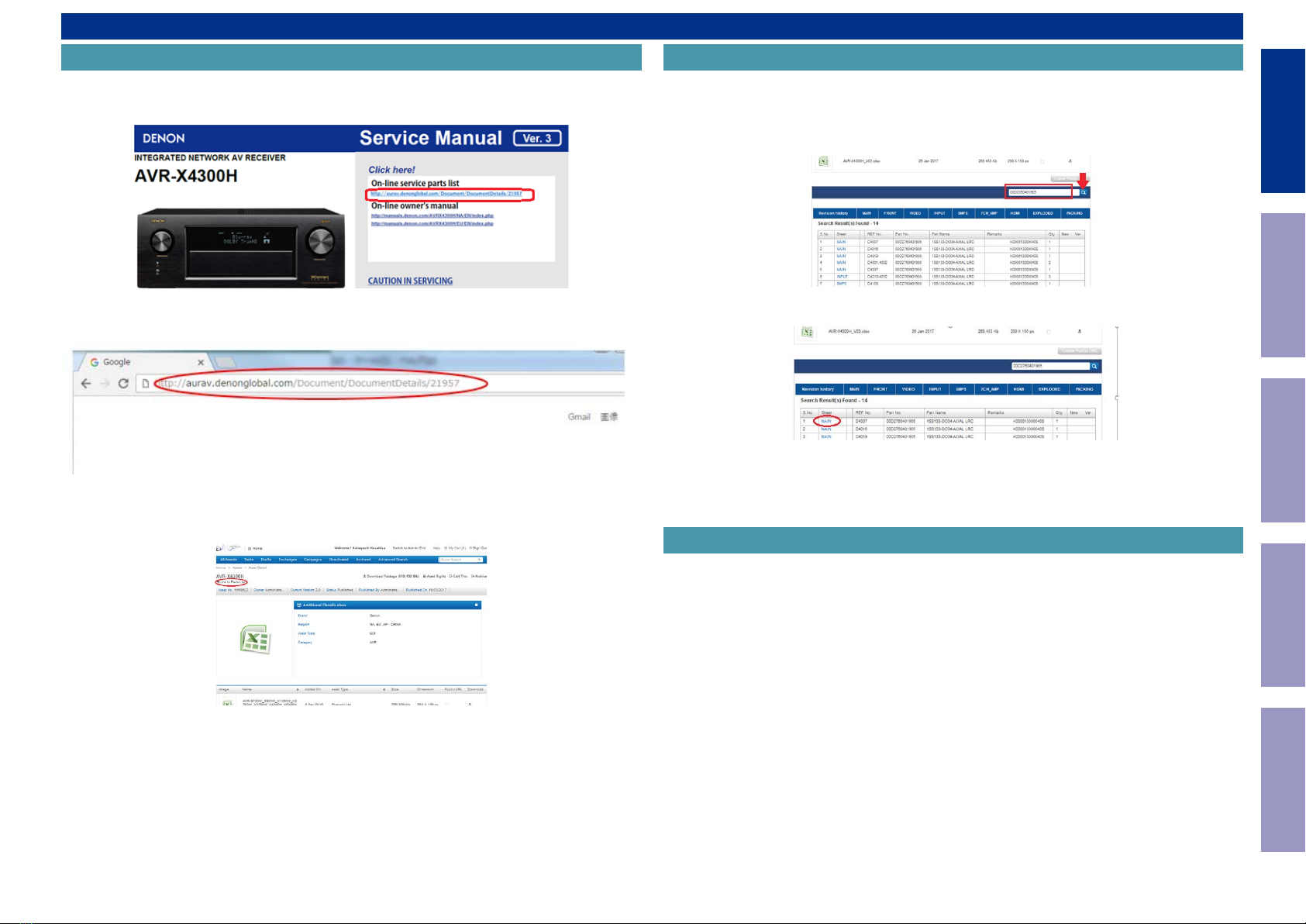
This Unit Electrical Mechanical Repair Information Updating
4