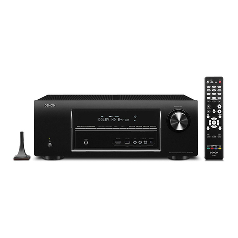
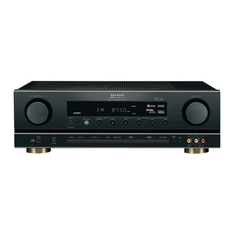
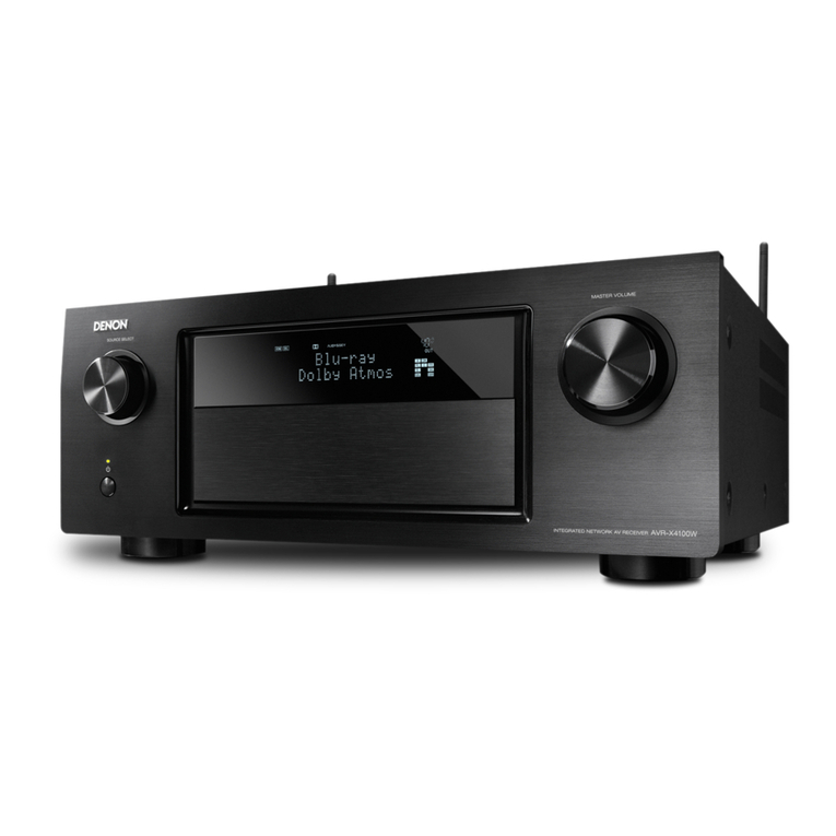
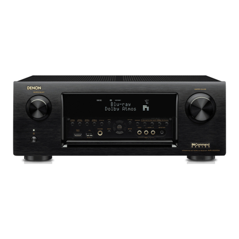
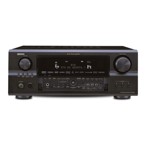
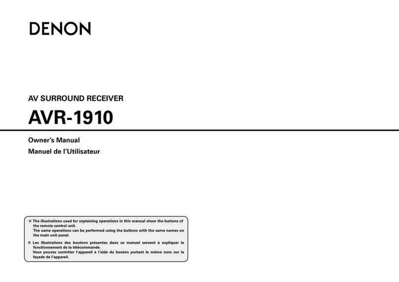
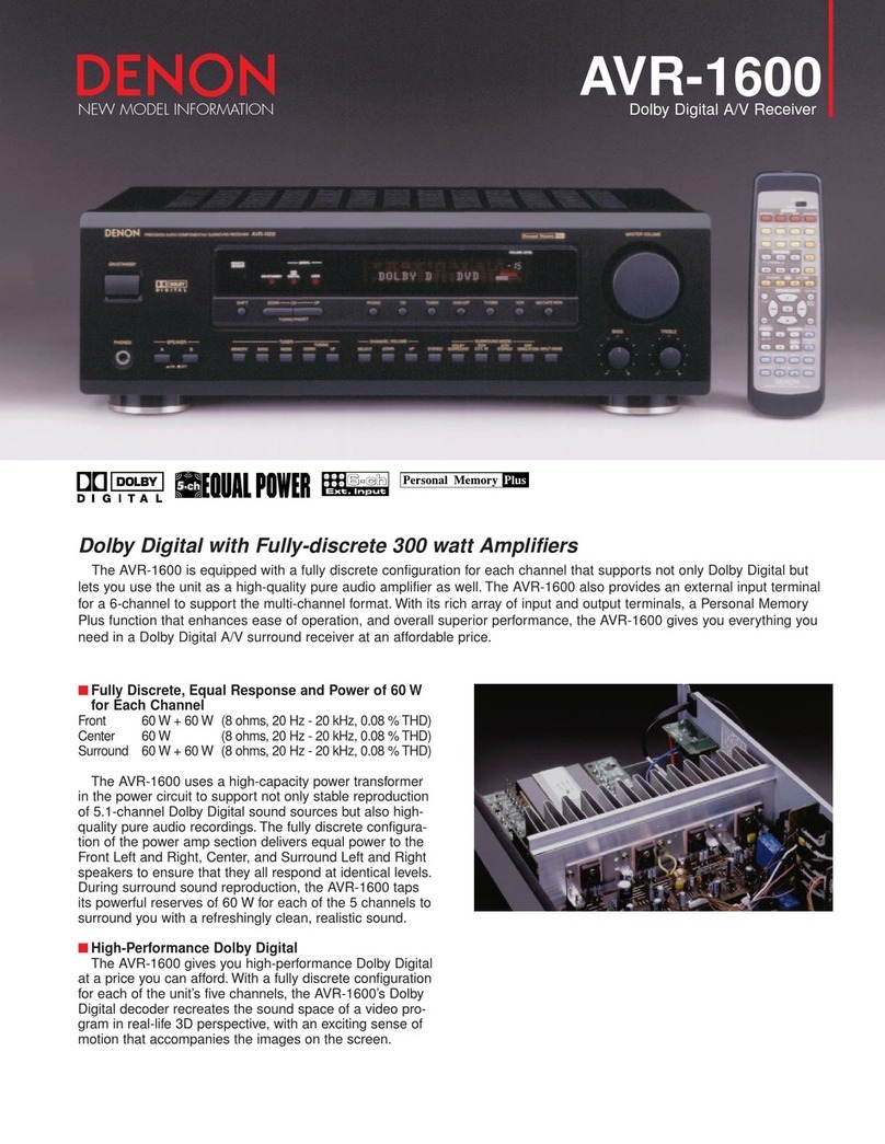
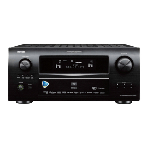
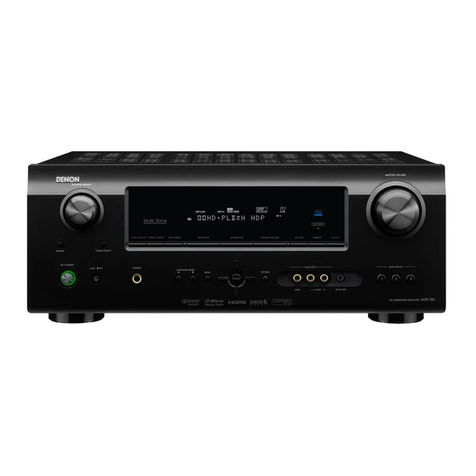
Denon AVR-4208 User manual

Hi-Fi Component
SERVICE MANUAL
MODEL
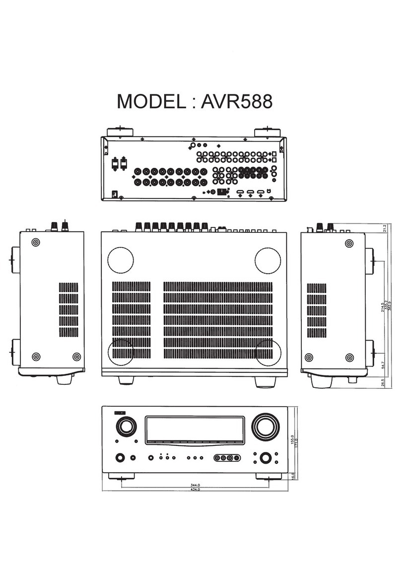
AVR-4802
MODEL
AVC-A11SR
AV SURROUND RECEIVER / AMPLIFIER
Some illustrations using in this service manual are slightly different from the actual set.
For U.S.A., Canada, Europe,
Asia, China, Hong Kong,
Korea & Taiwan R.O.C. model
14-14, AKASAKA 4-CHOME, MINATO-KU, TOKYO 107-8011 JAPAN
Telephone: 03 (3584) 8111
X0120 1174 NC 0108
For AVR-4802 For AVC-A11SR
w
w
w
.
x
i
a
o
y
u
1
6
3
.
c
o
m
Q
Q
3
7
6
3
1
5
1
5
0
9
9
2
8
9
4
2
9
8
T
E
L
1
3
9
4
2
2
9
6
5
1
3
9
9
2
8
9
4
2
9
8
0
5
1
5
1
3
6
7
3
Q
Q
TEL 13942296513 QQ 376315150 892498299
http://www.xiaoyu163.com
2
AVR-4802/AVC-A11SR
SAFETY PRECAUTIONS
The following check should be performed for the continued protection of the customer and service technician.
LEAKAGE CURRENT CHECK
Before returning the unit to the customer, make sure you make either (1) a leakage current check or (2) a line to chassis
resistance check. If the leakage current exceeds 0.5 milliamps, or if the resistance from chassis to either side of the
power cord is less than 460 kohms, the unit is defective.
SPECIFICATIONS
Audio Section
Power amplifier:
Rated output: Stereo (2 ch driven)
(All properties shown are only for the 125 W + 125 W (8 Ω/ohms, 20 Hz ~ 20 kHz with 0.05 % T.H.D.)
power amplifer stage.) 150 W + 150 W (6 Ω/ohms, 20 Hz ~ 20 kHz with 0.05 % T.H.D.)
Dynamic power: 170 W ×2 ch (8 Ω/ohms)
270 W ×2 ch (4 Ω/ohms)
350 W ×2 ch (2 Ω/ohms)
Output terminals: Front/Center: 6 ~ 16 Ω/ohms
Surround: A or B 6 ~ 16 Ω/ohms
A + B 8 ~ 16 Ω/ohms
Analog:
Input sensitivity/input impedance: 200 mV/47 kΩ/kohms
Frequency response: 10 Hz ~ 100 kHz: +0, −3 dB (DIRECT mode)
S/N: 105 dB (DIRECT mode)
Distortion: 0.005 % (20 Hz ~ 20 kHz) (DIRECT mode)
Rated output/maximum output: 1.2 V/8 V
Digital:
D/A output: Rated output 2 V (at 0 dB playback)
Total harmonic distortion 0.005 % (1 kHz, at 0 dB)
S/N ratio 110 dB
Dynamic range 108 dB
Digital input: Format Digital audio interface
Phono equalizer (PHONO input
REC OUT):
Input sensitivity: 2.5 mV
RIAA deviation: ±1 dB (20 Hz to 20 kHz)
Signal-to-noise ratio: 74 dB (A weighting, with 5 mV input)
Rated output/Maximum output: 150 mV/8V
Distortion factor: 0.03 % (1 kHz, 3 V)
Video Section
Standard video jacks
Input/output level and impedance: 1 Vp-p, 75 Ω/ohms
Frequency response: 5 Hz ~ 10 MHz +0, −3 dB
S-video jacks
Input/output level and impedance: Y (brightness) signal 1 Vp-p, 75 Ω/ohms
C (color) signal 0.286 Vp-p, 75 Ω/ohms
Frequency response: 5 Hz ~ 10 MHz +0, −3 dB
Color component video terminal:
Input/output level and impedance: Y (brightness) signal 1 Vp-p, 75 Ω/ohms
PB/CB(blue) signal 0.7 Vp-p, 75 Ω/ohms
PR/CR(red) signal 0.7 Vp-p, 75 Ω/ohms
Frequency response: DC ~ 50 MHz +0, −3 dB
Tuner Section
[FM] (note: µV at 75 Ω/ohms, 0 dBf = 1 ×10-15 W) [AM]
Receiving range: 87.5 MHz ~ 107.9 MHz 520 kHz ~ 1710 kHz
Usable sensitivity: 1.0 µV (11.2 dBf) 18 µV
50 dB Quieting sensitivity: MONO 1.6 µV (15.3 dBf)
STEREO 23 µV (38.5 dBf)
Signal to Noise Ratio (IHF-A): MONO 77 dB 50 dB
STEREO 72 dB
Total Harmonic Distortion (at 1 kHz): MONO 0.15 %
STEREO 0.3 %
General
Power supply: AC 120 V, 60 Hz (U.S.A., Canada & Taiwan R.O.C. model)
AC 230 V, 50 Hz (Europe & Asia model)
AC 220 V, 50 Hz (China model)
Power consumption: 10.5 A (U.S.A., & Canada model)
Maximum external dimensions: 434 (W) ×179 (H) ×485 (D) mm (17-3/32″×7-3/64″×19-3/32″)
Mass: 20.5 kg (45 lbs 3.1 oz)
Remote Control Unit (RC-8000): AVR Model only
Batteries: LR6/AA Type (four batteries)
External dimensions: 96 (W) ×38 (H) ×168.5 (D) mm (3-25/32″×1-1/2″×6-41/64″)
Mass: 242 g (Approx. 8.5 oz) (not including batteries)
Remote Control Unit (RC-899): AVC Model only
Batteries: R6P/AA Type (three batteries)
External dimensions: 61 (W) ×230 (H) ×34 (D) mm (2-13/32″×9-1/16″×1-11/32″)
Mass: 150 g (Approx. 5.3 oz) (not including batteries)
* For purposes of improvement, specifications and design are subject to change without notice.
w
w
w
.
x
i
a
o
y
u
1
6
3
.
c
o
m
Q
Q
3
7
6
3
1
5
1
5
0
9
9
2
8
9
4
2
9
8
T
E
L
1
3
9
4
2
2
9
6
5
1
3
9
9
2
8
9
4
2
9
8
0
5
1
5
1
3
6
7
3
Q
Q
TEL 13942296513 QQ 376315150 892498299
http://www.xiaoyu163.com
3
AVR-4802/AVC-A11SR
WIRE ARRANGEMENT
If wire bundles are untied or moved to perform adjustment or parts replacement etc.,be sure to rearrange them neatly as they
were originally bundled or placed afterward.
Otherwise, incorrect arrangement can be a cause of noise generation.
Wire arrangement viewed from the top
Back Panel side
Front Panel side
CAUTION IN SERVICING
When you have replaced the 1U-3291 Unit, or changed the CPU, DSP, or their peripheral parts, be sure to perform “RESET”
by pressing S803 on the DSP Unit Ass’y in the state of Standby or Power-on.
w
w
w
.
x
i
a
o
y
u
1
6
3
.
c
o
m
Q
Q
3
7
6
3
1
5
1
5
0
9
9
2
8
9
4
2
9
8
T
E
L
1
3
9
4
2
2
9
6
5
1
3
9
9
2
8
9
4
2
9
8
0
5
1
5
1
3
6
7
3
Q
Q
TEL 13942296513 QQ 376315150 892498299
http://www.xiaoyu163.com
5
AVR-4802/AVC-A11SR
DISASSEMBLY
(Follow the procedure below in reverse order when reassembling)
Top Cover
(1) Remove 9 screws 1on both sides and on the top.
(2) Remove 4 screws 2on the rear and detach the Top
Cover by sliding to the arrow direction.
Front Panel
(1) Remove 11 screws 3and detach the Bottom Cover.
(2) Remove the screw 4, 7 screws 5.
(3) Disconnect FFC wire from its connector, and detach
the Front Panel in the arrow direction.
Top Cover
2
1
1
Front Panel
1
1
2
3
4
5
5
5
FFC Wire
w
w
w
.
x
i
a
o
y
u
1
6
3
.
c
o
m
Q
Q
3
7
6
3
1
5
1
5
0
9
9
2
8
9
4
2
9
8
T
E
L
1
3
9
4
2
2
9
6
5
1
3
9
9
2
8
9
4
2
9
8
0
5
1
5
1
3
6
7
3
Q
Q
TEL 13942296513 QQ 376315150 892498299
http://www.xiaoyu163.com
6
AVR-4802/AVC-A11SR
P.W.B.s on Front Panel
(1) FLD P.W.B.
Remove 6 screws 6.
(2) Tact SW P.W.B.
Remove 10 screws 7after taking off the select knob
and nut.
(3) Master VR P.W.B.
Remove the screw 8after taking off the master volume
knob and nut.
(4) Power SW P.W.B.
Remove 2 screws 9.
(5) Remo-con. P.W.B.
Remove the screw 10 after taking off the input selector
knob and nut.
S. Video P.W.B. / C. Video P.W.B. / Comp
Video P.W.B. / Audio P.W.B. Block
(1) Disconnect the FFC from its connector.
(2) Remove 6 screws
11
, 3 screws 12 , 53 screws 13 , 2
screws 14 , and detach the Back Panel.
(3) Remove 16 screws 15 of the wires connecting to the
C. Video P.W.B.
(4) Remove 2 screws 16 .
Front
Rear
C.Video P.W.B. (Top view)
Tact SW P.W.B.
8
Master Volume
P.W.B.
7
6
6
10
Select Knob
9
Master Volume Knob
FLD P.W.B.Input Selector Knob
Remo-con. P.W.B.
Power SW
P.W.B.
FFC Wire
Back Panel
11
11
12
13
13
13
13
13
14
15
16
15
16
13
w
w
w
.
x
i
a
o
y
u
1
6
3
.
c
o
m
Q
Q
3
7
6
3
1
5
1
5
0
9
9
2
8
9
4
2
9
8
T
E
L
1
3
9
4
2
2
9
6
5
1
3
9
9
2
8
9
4
2
9
8
0
5
1
5
1
3
6
7
3
Q
Q
TEL 13942296513 QQ 376315150 892498299
http://www.xiaoyu163.com
7
AVR-4802/AVC-A11SR
17
P.W.B. Block
Remove P.W.B.s in the following order.
1. Connect L P.W.B.
2. Comp. Video P.W.B.
3. S Video P.W.B./C Video & Reg. P.W.B./OSD P.W.B.
4. Audio In P.W.B.
5. DSP P.W.B.
COMP. VIDEO P.W.B.
232C P.W.B.
CONNECT L P.W.B.
DSP P.W.B.
PHONO P.W.B.
AUDIO IN P.W.B.
S VIDEO P.W.B.
CONNECT R P.W.B.
C VIDEO & REG. P.W.B.
OSD P.W.B.
Power AMP L/R P.W.B.
(1) Remove 8 screws 17 fastening to the chassis.
17
17
17
w
w
w
.
x
i
a
o
y
u
1
6
3
.
c
o
m
Q
Q
3
7
6
3
1
5
1
5
0
9
9
2
8
9
4
2
9
8
T
E
L
1
3
9
4
2
2
9
6
5
1
3
9
9
2
8
9
4
2
9
8
0
5
1
5
1
3
6
7
3
Q
Q
TEL 13942296513 QQ 376315150 892498299
http://www.xiaoyu163.com

8
AVR-4802/AVC-A11SR
Front Chassis
Front Chassis, H/P P.W.B.
(1) Remove 8 screws 18 .
(2) Detach the Front Chassis by pulling upward to release
4 hooks.
(3) Remove 2 screws 19 and snap plate, then detach the
H/P P.W.B.
Hook
18
18
18
Hook
19
19
Snap Plate H/P P.W.B.
w
w
w
.
x
i
a
o
y
u
1
6
3
.
c
o
m
Q
Q
3
7
6
3
1
5
1
5
0
9
9
2
8
9
4
2
9
8
T
E
L
1
3
9
4
2
2
9
6
5
1
3
9
9
2
8
9
4
2
9
8
0
5
1
5
1
3
6
7
3
Q
Q
TEL 13942296513 QQ 376315150 892498299
http://www.xiaoyu163.com
9
AVR-4802/AVC-A11SR
CH1: IC104 (5)
1
CH1: 64fs
CH2: fs
CH3: 256fs
CH4:
FRONT DATA
3
CH1: DATA
CH2: fs
CH3: 64fs
2
CLOCK FLOW & WAVE FORM IN DIGITAL BLOCK
Clock Flow Wave Form
IC512
1
SN74LV4040APW
INPUT
SELECTOR (9) (3) (11) (2)MCLK
(10) (7) (26)BCLK
IC104 (13) (25)LRCLK
SN74HC (10) (27)SDATA
151APW CKOUT(13) FRONTch
(5) (5)DIN2 BCK(14)
LRCK(15)
DATAD(16)
XIN(22)
12.287MHz
IC113 (2)MCLK
SG-8002 (7) (26)BCLK
(13) (25)LRCLK
(3) (10) (27)SDATA
IC112 CENTERch
SN74LV4040APW (2) (13) (4) (15) (7) (18) (8) (19) SUBWOOFERch
RFS0 RFS1 RCLK0 RCLK1 TFS0 TFS1 TCLK0 TCLK1
MCLK(17) TCLK0(8) (4)RCLK0
AIN SCLK(18) TCLK1(19) (15)RCLK1
LRCK(19) (2)MCLK
SDATA(21) TFS0(7) (2)RFS0 (26)BCLK
TFS1(18) (13)RFS1 (25)LRCLK
(27)SDATA
(5)DR0A DT0A(11) (5)DR0A DT0A(11)
DT0B(12) (6)DR0B DT0B(12) SURROUNDch
DT1A(22) (16)DR1A DT1A(22)
DT1B(23) (17)DR1B DT1B(23)
(2)MCLK
(26)BCLK
(25)LRCLK
(27)SDATA
SURROUND BACKch
DIR
IC111
LC89055W
A/D CONVERTER
AD1854K
IC114
AK5353VS
IC107
74LVX157MTC
2nd DSP1st DSP
A/D SELECTOR
IC502
ADSP-21065L
IC501
ADSP-21065L
IC511
D/A CONVERTER
IC305
AD1854K
IC307
IC301
AD1854K
IC303
AD1854K
SYNC
SN74LV86APW
SN74LV00APW
IC523
256fs
64fs
fs
DATA
DATA
256fs
64fs
fs
FRONT
CENTER/SW
SURROUNDSURROUND BACK
fs
64fs
2
3
DOLBY DIGITAL Decode
DTS-ES Decode
AL24 Processing
THX Filter Processing
EX/ES Matrices Processing
Sound Simulation
Bus-Management Processing
* fs is a sampling frequency of input digital signal.
e.g.: sampling frequency 48 kHz →fs=48 kHz
* 64fs and 256fs are 64 or 256 times the sampling frequency
respectively.
e.g.:sampling frequency 48 kHz
64fs:48kHz x 64 = 3.072MHz
256fs:48kHz x 256 = 12.288MHz
* The sampling frequency for analog input is fixed to 48kHz internally.
* (No.) indicates the pin number of individual IC.
* The arrow indicates the direction of signal flow. As the input terminal
pointed by the arrowhead and the output terminal by the opposite.
ClockWave.p65 01/08/02, 20:39Page 8-9 AdobePageMaker6.5J/Win
w
w
w
.
x
i
a
o
y
u
1
6
3
.
c
o
m
Q
Q
3
7
6
3
1
5
1
5
0
9
9
2
8
9
4
2
9
8
T
E
L
1
3
9
4
2
2
9
6
5
1
3
9
9
2
8
9
4
2
9
8
0
5
1
5
1
3
6
7
3
Q
Q
TEL 13942296513 QQ 376315150 892498299
http://www.xiaoyu163.com
12
AVR-4802/AVC-A11SR
ADJUSTMENT
Audio Section
Idling Current (1U-3356-1, 2)
Required measurement equipment : DC Voltmeter
Preparation
(1) Avoid direct blow from an air conditioner or an electric fan, and adjust the unit at normal room tempereture 15 °C ~ 30 °C
(59 °F ~ 86 °F).
(2) Presetting
POWER (Power source switch) →OFF
SPEAKER (Speaker terminal) →No load (Do not connect speaker, dummy resistor, etc.)
Adjustment
(1) Remove top cover and set VR101, VR301, VR401 on 1U-3356-1 (Power Amp L unit), VR102, VR202, VR302, VR402 on
1U-3356-2 (Power Amp. R Unit) at fully counterclockwise ( ) position.
(2) Connect DC Voltmeter to test points (FRONT-Lch: TP101, FRONT-Rch: TP102, CENTER ch: TP202, SURROUND-Lch:
TP301, SURROUND-Rch: TP302, SURROUND BACK-Lch: TP401, SURROUND BACK-Rch: TP402).
(3) Connect power cord to AC Line, and turn power switch "ON".
(4) Presetting. MASTER VOLUME : "---" counterclockwise ( min.)
MODE : 5CH/7CH STEREO
FUNCTION : CD
(5) Within 2 minutes after the power on, turn VR101 clockwise ( ) to adjust the TEST POINT voltage to 2 mV ±0.5 mV DC.
(6) After 10 minutes from the preset above, turn VR101 to set the voltage to 2 mV ±0.5 mV DC.
(7) Adjust the Variable Resistors of other channels in the same way.
1U-3356-1
VR402
TP402
1U-3356-2
Power Trans
VR302
TP302
VR102
TP102
VR401
TP401
VR301
TP301
VR101
TP101
DC Voltmeter
VR202
TP202
w
w
w
.
x
i
a
o
y
u
1
6
3
.
c
o
m
Q
Q
3
7
6
3
1
5
1
5
0
9
9
2
8
9
4
2
9
8
T
E
L
1
3
9
4
2
2
9
6
5
1
3
9
9
2
8
9
4
2
9
8
0
5
1
5
1
3
6
7
3
Q
Q
TEL 13942296513 QQ 376315150 892498299
http://www.xiaoyu163.com
13
AVR-4802
13
AVR-4802/AVC-A11SR
SEMICONDUCTORS
IC’s
LH28F800BVE-BTL90 (IC504, 507)
1
2
3
4
5
6
7
8
9
10
11
12
13
14
15
16
17
18
19
20
21
22
23
24 25
26
27
28
29
30
31
32
33
34
35
36
37
38
39
40
41
42
43
44
45
46
47
48
A15
A14
A13
A12
A11
A10
A9
A8
NC
NC
WE
RESET
NC
NC
RDY/BSY
A18
A17
A7
A6
A5
A4
A3
A2
A1
A16
BYTE
V
SS
DQ15/A-1
DQ7
DQ14
DQ6
DQ13
DQ5
V
DD
DQ11
DQ3
DQ10
DQ2
DQ9
DQ0
OE
V
SS
CE
A0
DQ1
DQ8
DQ12
DQ4
D
Q
L
D
Q
L
D
Q
L
D
Q
L
D
Q
L
D
Q
L
D
Q
L
D
Q
L
D0 D1 D2 D3 D4 D5 D6 D7
LE
OE 1
234 5678
9
11
121314
1516
17
1819
Q0 Q1 Q2 Q3 Q4 Q5 Q6 Q7
S
N74AHCT573PW (IC516, 520)
S
N74LV573ANS (IC517, 521)
1
2
3
4
5
6
7
8
9
10
20
19
18
17
16
15
14
13
12
11
OE
D0
D1
D2
D3
D4
D5
D6
D7
GND
Vcc
Q0
Q1
Q2
Q3
Q4
Q5
Q6
Q7
LE
1
2
3
4
5
6
7
8
9
10
11
12
13
14
15
16
17
18
19
20
21
22 23
24
25
26
27
28
29
30
31
32
33
34
35
36
37
38
39
40
41
42
43
44
A4
A3
A2
A1
A0
CE
I/O 1
I/O 2
I/O 3
I/O 4
V
DD
GND
I/O 5
I/O 6
I/O 7
I/O 8
WE
A15
A14
A13
A12
N.C.
A5
A6
A7
OE
B
LB
I/O 1 6
I/O 1 5
I/O 1 4
I/O 1 3
GND
V
DD
I/O 1 2
I/O 1 1
I/O 1 0
I/O 9
N. .
A8
A9
A10
A11
N.C.
16MB SDRAM TSOP-8 H/W (IC505, 506, 508, 509)
Symbol Function
A0~A18 Address input
DQ0~DQ14 Data in/output
DQ15/A-1 Data in/output/Address input
CE Chip enable input
OE Output enable input
BYTE Word/byte select input
WE Write enable input
RDY/BSY Ready/busy output
RESET Hardware reset input
N.C. No connection
VDD Power
Vss GND
Symbol Function
A0~A15 Address input
I/O1~I/O16 Data in/output
CE Chip enable input
WE Write enable input
OE Output buffer control input
LB, UB Data byte control input
VDD Power terminal (3.3V)
GND GND
N.C. No connection
N.U. Unusable (input)
w
w
w
.
x
i
a
o
y
u
1
6
3
.
c
o
m
Q
Q
3
7
6
3
1
5
1
5
0
9
9
2
8
9
4
2
9
8
T
E
L
1
3
9
4
2
2
9
6
5
1
3
9
9
2
8
9
4
2
9
8
0
5
1
5
1
3
6
7
3
Q
Q
TEL 13942296513 QQ 376315150 892498299
http://www.xiaoyu163.com
14
AVR-4802/AVC-A11SR
ADSP-21065L (IC501, 502)
Pin Name
ADSP-21065L Terminal Function
Pin
No. Pin Name
Pin
No.
Pin Name
Pin
No.
Pin Name
Pin
No.
Pin Name
Pin
No.
Pin Name
Pin
No.
1 VDD
2 RFS0
3 GND
4 RCLK0
5 DR0A
6 DR0B
7 TFS0
8 TCLK0
9 VDD
10 GND
11 DT0A
12 DT0B
13 RFS1
14 GND
15 RCLK1
16 DR1A
17 DR1B
18 TFS1
19 TCLK1
20 VDD
21 VDD
22 DT1A
23 DT1B
24
PWM_EVENT1
25 GND
26
PWM_EVENT0
27 BR1
28 BR2
29 VDD
30 CLKIN
31 XTAL
32 VDD
33 GND
34 SDCLK1
35 GND
36 VDD
37 SDCLK0
38 DMAR1
39 DMAR2
40 HBR
41 GND
42 RAS
43 CAS
44 SDWE
45 VDD
46 DQM
47 SDCKE
48 SDA10
49 GND
50 DMAG1
51 DMAG2
52 HBG
53 BMSTR
54 VDD
55 CS
56 SBTS
57 GND
58 WR
59 RD
60 GND
61 VDD
62 GND
63 REDY
64 SW
65 CPA
66 VDD
67 VDD
68 GND
69 ACK
70 MS0
71 MS1
72 GND
73 GND
74 MS2
75 MS3
76 FLAG11
77 VDD
78 FLAG10
79 FLAG9
80 FLAG8
81 GND
82 DATA0
83 DATA1
84 DATA2
85 VDD
86 DATA3
87 DATA4
88 DATA5
89 GND
90 DATA6
91 DATA7
92 DATA8
93 VDD
94 GND
95 VDD
96 DATA9
97 DATA10
98 DATA11
99 GND
100 DATA12
101 DATA13
102 NC
103 NC
104 DATA14
105 VDD
106 GND
107 DATA15
108 DATA16
109 DATA17
110 VDD
111 DATA18
112 DATA19
113 DATA20
114 GND
115 NC
116 DATA21
117 DATA22
118 DATA23
119 GND
120 VDD
121 DATA24
122 DATA25
123 DATA26
124 VDD
125 GND
126 DATA27
127 DATA28
128 DATA29
129 GND
130 VDD
131 VDD
132 DATA30
133 DATA31
134 FLAG7
135 GND
136 FLAG6
137 FLAG5
138 FLAG4
139 GND
140 VDD
141 VDD
142 NC
143 ID1
144 ID0
145 EMU
146 TDO
147 TRST
148 TDI
149 TMS
150 GND
151 TCK
152 BSEL
153 BMS
154 GND
155 GND
156 VDD
157 RESET
158 VDD
159 GND
160 ADDR23
161 ADDR22
162 ADDR21
163 VDD
164 ADDR20
165 ADDR19
166 ADDR18
167 GND
168 GND
169 ADDR17
170 ADDR16
171 ADDR15
172 VDD
173 ADDR14
174 ADDR13
175 ADDR12
176 VDD
177 GND
178 ADDR11
179 ADDR10
180 ADDR9
181 GND
182 VDD
183 ADDR8
184 ADDR7
185 ADDR6
186 GND
187 GND
188 ADDR5
189 ADDR4
190 ADDR3
191 VDD
192 VDD
193 ADDR2
194 ADDR1
195 ADDR0
196 GND
197 FLAG0
198 FLAG1
199 FLAG2
200 VDD
201 FLAG3
202 NC
203 NC
204 GND
205 IRQ0
206 IRQ1
207 IRQ2
208 NC
1
53
52 104
105
156
157208
w
w
w
.
x
i
a
o
y
u
1
6
3
.
c
o
m
Q
Q
3
7
6
3
1
5
1
5
0
9
9
2
8
9
4
2
9
8
T
E
L
1
3
9
4
2
2
9
6
5
1
3
9
9
2
8
9
4
2
9
8
0
5
1
5
1
3
6
7
3
Q
Q
TEL 13942296513 QQ 376315150 892498299
http://www.xiaoyu163.com
TMP95FY64F (IC801)
75
76
100
125
26
50
51
TMP95FY64F Terminal Function
Pin.
No. Name
1 VREFL VREFL
A/D ref. GND
2 AVss AVss
A/D GND
3 AVcc AVcc
AD +5V
4 DAOUT0 DAOUT0 No connection
5 DAOUT1 DAOUT1 O C
Od L L No connection
6 _NMI _NMI I
Not used (fixed to H)
7 P53/_BUSRQ ASIC RESET O N
Eu H H ASIC control terminal (L: Reset)
8 P54/_BUSAK WP1 O C
Od Memory write protect for DSP1
9 P55/_WAIT WP2 O C
Od Memory write protect for DSP2
10 P56/INT0 B.DOWN I
E
↓
&L Eu Z
Power down detect (L: Detected)
11 P57/SCLK2/_CTS2 ROM_RES1 O C
Od Memory reset for DSP1
12 P80/TxD0 MISO O C MAIN-SUB
µ
com comm. control terminal (Data out)
13 P81/RxD0 MOSI I
MAIN-SUB
µ
com comm. control terminal (Data in)
14 P82/SCLK0/_CTS0 CLK I/O C MAIN-SUB
µ
com comm. control terminal (I2C clock in/out)
15 P83/TxD1 DIR MOSI O C
Z L DIR control terminal (LC89055Q), control data output
16 P84/RxD1 DIR MISO I
Lv
DIR control input terminal (LC89055Q), control data input
17 P85/SCLK1/_CTS1 DIR CLK O C
Z L DIR control terminal (LC89055Q), control clock output
18 P86/TxD2 TxD O C
Z L Data send output to external (common with 1394 data comm.)
19 P87/RxD2 RxD I
Lv
Data receive input from external (common with 1394 data comm.)
20 P60/_CS0 D.EXP OE O C
Z L Port Expander control out for DIGITAL input switching (TC4094B)
21 P61/_CS1 D.EXP CLK O C
Z L Port Expander control out for DIGITAL input switching (TC4094B)
22 P62/_CS2 D.EXP DATA O C
Z L Port Expander control out for DIGITAL input switching (TC4094B)
23 P63/_CS3 D.EXP STB O C
Z L Port Expander control out for DIGITAL input switching (TC4094B)
24 CLK CLK O C
Eu
25 Vcc Vcc
+5V
26 Vss I/O1
GND
27 X1 Xin I
X'tal connection
28 X2 Xout O
X'tal connection
29 _EA _EA
Fixed to +5V
30 _RESET RESET I
Lv Eu L
Reset input
31 P70/TI0/INT1 DSP ACK1 I
E
↑
&L
DSP1 host interface comm. respond input (L: OK)
32 P71/TO1 _DSP1 RESET O C
Od L L DSP1 reset output terminal (L: Reset)
33 P72/TO3/INT2 AC-3 RF DET. I
E
↓
&L
AC-3 RF signal detect input (L: AC-3 RF signal input)
34 P73/TI4/INT3 DAC-192 O C
Sets D/A to 192k
35 P74/TO5 _DSP2 RESET O C
Od L L DSP2 reset output terminal (L: Reset)
36 P75/TO7/INT4 _REQ O C
Eu H L MAIN-SUB
µ
com comm. control terminal (L: Comm. request from SUB)
37 P90/TI8/INT5 _ACK I
E
↓
&L Eu
MAIN-SUB
µ
com comm. control terminal (L: Ack. return from MAIN)
38 P91/TI9/INT6 CSI I
Lv
DIR control input terminal (LC89055Q), L: PCM
39 P92/TO8 EMP I
Lv
H: EMP ON
40 P93/TO9 DEEPM O C
Ed L L
41 P94/TIA/INT7 _CS I
E
↑
&L Od
DIR control input terminal (LC89055Q), L
→
H: Cannel status change
42 P95/TIB/INT8 ERR I
E
↑
&L
DIR control input terminal (LC89055Q), H: ERR
43 P96/TOA/TOB DIR RESET O C
Z L DIR control input terminal (LC89055Q), L: Reset
44 Vcc Vcc
+5V
45 P00/D0 DIT_RESET C
Z L DIT control terminal
46 P01/D1 DIT CLK C
Z L DIT control terminal
47 P02/D2 DIT uDATA C
Z L DIT control terminal
48 P03/D3 DIT ST C
Z L DIT control terminal
49 P04/D4 DIT_CS C
Z L DIT control terminal
50 P05/D5 DIT R/W C
Z L DIT control terminal
51 P06/D6 DH/RESET C
Z L DHIVA board reset (fixed to L)
Symbol I/O Type Det Op Res Ini Function
Pin.
No. Name Symbol I/O Type Det Op Res Ini Function
52 P07/D7 DMUTE C
Z L Digital input MUTE control output (same control as SELCK)
53 P10/D8 I/O1 I/O C
Z L DSP comm. terminal (ADSP21061L:D16)
54 P11/D9 I/O2 I/O C
Z L DSP comm. terminal (ADSP21061L:D17)
55 P12/D10 I/O3 I/O C
Z L DSP comm. terminal (ADSP21061L:D18)
56 P13/D11 I/O4 I/O C
Z L DSP comm. terminal (ADSP21061L:D19)
57 P14/D12 I/O5 I/O C
Z L DSP comm. terminal (ADSP21061L:D20)
58 P15/D13 I/O6 I/O C
Z L DSP comm. terminal (ADSP21061L:D21)
59 P16/D14 I/O7 I/O C
Z L DSP comm. terminal (ADSP21061L:D22)
60 P17/D15 I/O8 I/O C
Z L DSP comm. terminal (ADSP21061L:D23)
61 AM8/_16 Fixed to +5V
62 Vss Vss
GND
63 Vcc Vcc
+5V
64 P27/A23 _DSP REQUEST1 O C
ZL
DSP1 (ADSP21061L-A:IRQ 1_) host interface interrupt req. output, L: REQ
65 P26/A22 WRITE1 O C
Z L DSP1 comm. control terminal (H: DATA WRITE)
66 P25/A21 _DSP REQUEST2 O C
ZL
DSP2 (ADSP21061L-A:IRQ 1_) host interface interrupt req. output, L: REQ
67 P24/A20 WRITE2 O C
Z L DSP2 comm. control terminal (H: DATA WRITE)
68 P23/A19 DSP ACK2 I
E
↑
&L
DSP2 host interface comm. respond input (L: OK)
69 P22/A18 BUSY2 I
Lv
DSP busy check flag (ADSP21061L-B:FLAG 2B) input, L: Normal
70 P21/A17 FLAG 3A I
Lv
Special flag for ROM update (ADSP21061L-A:FLAG 3A)
71 P20/A16 BUSY1 I
Lv
DSP busy check flag (ADSP21061L-A:FLAG 2A) input, L: Normal
72 P37/A15 SEL CK O C
Z L ADC/DIR data/clock switching control terminal (L: ADC)
73 P36/A14 DIR CE O C
Z L DIR control terminal (LC89055Q), control chip enable output
74 P35/A13 FLAG 3B I
Lv
Special flag for ROM update (ADSP21061L-A:FLAG 3B)
75 P34/A12 DAC-RESET2 O C
Od L H DAC control terminal (L: Power down,
↑
: Reset, H: Normal)
76 P33/A11 DIGITAL POWER O C
Z L DIGITAL power ON/OFF switching
77 P32/A10 DIR AUTO O C
Od Z L
78 P31/A9 BPSYNC O C
ZL
79 P30/_B00T/A8 _B00T I
Lv Eu Z
Single Chip/Single Boot switching input (H & Reset: Single Chip Mode)
80 P47/A7 _DEMOD RESET O C
Od L L Demodulator reset output (L: Reset)
81 P46/A6 DEMOD ON O C
Od L L Demodulator osc. control output (H: Osc.)
82 P45/A5 FGAIN O C
Z L IV AMP GAIN switching control output (L: Sub-woofer on)
83 P44/A4 A/D RESET O N
Eu H H A/D control terminal (L: Reset)
84 P43/A3 DAC-RESET1 O C
Od L H DAC control terminal (L: Power down,
↑
: Reset, H: Normal)
85 P42/A2 DAC-DIF. DAC differential use: H
86 P41/A1 DIG. (AC3) MUTE O C
Od Z L Digital mute control output (L: AC-3 or DTS decode possible)
87 P40/A0 ERR MUTE_ O C
Od L L Pop noise preventive mute control output
88 P50/_RD DH IN O C
Z L For 1394 (fixed to L)
89 P51/_WR DH OUT O C
Z L For 1394 (fixed to L)
90 P52/_HWR ROM_RES2 O C
Od Memory reset for DSP2
91 Vss Vss
GND
92 PA0/AN0 96K DET I
Lv
96k signal detect input, H: 96k
93 PA1/AN1 DHERR I
Lv
DHIVA board error input (fixed to L)
94 PA2/AN2 I
Lv
Not used (Pull down)
95 PA3/AN3/_ADTRG Not used (Pull down)
96 PA4/AN4 I
Lv
Not used (Pull down)
97 PA5/AN5 I
Lv
Not used (Pull down)
98 PA6/AN6 I
Lv
Not used (Pull down)
99 PA7/AN7 MODE-0-SUB I
Lv
FLASH ROM rewrite mode input
100 VREFH VREFH
AD ref. +5V
Note: Pin No. : Terminal number of microcomputer.
Port Name : The name entered in the data sheet of microcomputer.
Symbol : Symbolized interface function.
I/O : Input or out of part.
“I” = Input port
“O” = Output port
Type : Composition of port in case of output port.
“C” = CMOS output
“N” = NMOS open drain output
“P” = PMOS open drain output
Op : Pull up/Pull down selection information.
“Iu” = Inner microcomputer pull up
“Id” = Inner microcomputer pull down
“Eu” = External microcomputer pull up
“Ed” = External microcomputer pull down
Det : Indicates judging state of input port. Level detection is “LV”; Edge detection is “Ed”; Detection by both shifting is “E&L”; Serial data
detection is “S” (Serial data output is also “S”).
Res : State at reset.
“H” = Outputs High Level at reset
“L” = Outputs Low Level at reset
“Z” = Becomes High impedance mode at reset
Ini : Initial output state.
Function : Function and logical level explanation of signals to be interface.
15
AVR-4802/AVC-A11SR
3TMP95FY64F.p65 01/08/02, 20:58Page 2-3 AdobePageMaker6.5J/Win
w
w
w
.
x
i
a
o
y
u
1
6
3
.
c
o
m
Q
Q
3
7
6
3
1
5
1
5
0
9
9
2
8
9
4
2
9
8
T
E
L
1
3
9
4
2
2
9
6
5
1
3
9
9
2
8
9
4
2
9
8
0
5
1
5
1
3
6
7
3
Q
Q
TEL 13942296513 QQ 376315150 892498299
http://www.xiaoyu163.com

TMP95FY64F (IC802)
75
76
100
125
26
50
51
TMP95FY64F Terminal Function
Pin.
No. Name Symbol I/O Type Det Op Res Ini Function
1 VREFL VREFL
A/D ref. GND
2 AVss AVss
A/D GND
3 AVcc AVcc
AD +5V
4 DAOUT0 DAOUT0 O
No connection
5 DAOUT1 DAOUT1 O
No connection
6 _NMI _NMI I
Not used (fixed to H)
7 P53/_BUSRQ ACK O C
Z
MAIN-SUB
µ
com comm. control terminal
8 P54/_BUSAK REQ I
Lv Eu Z
MAIN-SUB
µ
com comm. control terminal
9 P55/_WAIT PLFL DATA O C
Z L PLL & FL control terminal (LC72131 & LC7511NE)
10 P56/INT0 PROTECT I
E
↑
&L Ed Z
Protection detect input (H: Detected)
11 P57/SCLK2/_CTS2 PLFL CLK O C
Z L PLL & FL control terminal (LC72131 & LC7511NE)
12 P80/TxD0 PLL STB O C
Z L PLL control terminal (LC72131)
13 P81/RxD0 ERROR LED O C
Ed Z H Not used
14 P82/SCLK0/_CTS0
MULTI ROOM POWER
OC
Z L Power amp control terminal for MULTI ROOM (H: ON)
15 P83/TxD1 MOSI O C
Z L MAIN-SUB
µ
com comm. control terminal
16 P84/RxD1 MISO I
Lv
Z
MAIN-SUB
µ
com comm. control terminal
17 P85/SCLK1/_CTS1 CLK I/O (C)
Z
MAIN-SUB
µ
com comm. control terminal
18 P86/TxD2 TxD O C
Z L Data transfer terminal to external
19 P87/RxD2 RxD I
Lv
Z
Data receive terminal from external
20 P60/_CS0 FUNC/TONE CLK O C
Z L Clock output for Function switching/Tone IC control
21 P61/_CS1 FUNC/TONE DATA O C
Z L Data output for Function switching/Tone IC control
22 P62/_CS2 ST/MONO O C
Z L Stereo/Mono control signal (L: Stereo receive)
23 P63/_CS3 STANDBY O C
Ed Z H Standby LED drive output (H: Light)
24 CLK CLK O C
No connection
25 Vcc Vcc
+5V
26 Vss Vss
GND
27 X1 X1 I
X'tal connection
28 X2 X2 O
X'tal connection
29 _EA _EA I
Fixed to +5V
30 _RESET _RESET I
Lv Iu L
Reset input
31 P70/TI0/INT1 VIDEO POWER O C
Z L Video power ON/OFF switching (H: ON)
32 P71/TO1 DIGITAL POWER O C
Z L Digital power ON/OFF switching (H: ON)
33 P72/TO3/INT2 (VKK POWER) O
Z L Not used (-VKK power ON/OFF switching)
34 P73/TI4/INT3 SEL A (M) I
Lv Eu Z
Master VR turn detect input (Rotary encoder)
35 P74/TO5 SEL B (M) I
Lv Eu Z
Master VR turn detect input (Rotary encoder)
36 P75/TO7/INT4 (FAN CONTROL) O C
Z L Not used (Fan control for power Tr)
37 P90/TI8/INT5 B.DOWN I
E
↓
&L Eu Z
Power down detect (L: Detected)
38 P91/TI9/INT6 STEREO I
Lv Eu Z
Stereo detect (L: Received)
39 P92/TO8 TUNED I
Lv Eu Z
Tune detect (L: Tuned)
40 P93/TO9 S MONI.DET I
Lv Eu Z
S Monitor connection detect input (L: Connected)
41 P94/TIA/INT7 REMOCON I
E
↑
&L Ed Z
Remote control signal input
42 P95/TIB/INT8 S SIG.DET I
Lv Eu Z
S signal detect input (H: Signal input)
43 P96/TOA/TOB SYNC.DET I
Lv Eu Z
Sync. detect input (H: External sync.)
44 Vcc Vcc
+5V
45 P00/D0 POWER O C
Z H Power relay control output (H: ON)
46 P01/D1 V.EXP OE O C
Z L Port expander control output for video circuit (TC4094B)
47 P02/D2 V.EXP CLK O C
Z L Port expander control output for video circuit (TC4094B)
48 P03/D3 V.EXP DATA O C
Z L Port expander control output for video circuit (TC4094B)
49 P04/D4 V.EXP STB O C
Z L Port expander control output for video circuit (TC4094B)
50 P05/D5 SP.EXP OE O C
Z L Port expander control output for speaker output (TC4094B)
51 P06/D6 SP.EXP CLK O C
Z L Port expander control output for speaker output (TC4094B)
52 P07/D7 SP.EXP DATA O C
Z L Port expander control output for speaker output (TC4094B)
Pin.
No. Name Symbol I/O Type Det Op Res Ini Function
53 P10/D8 SP.EXP STB O C
Z L Port expander control output for speaker output (TC4094B)
54 P11/D9 A.EXP OE O C
Z L Port expander control output for audio mute and relay control (TC4094B)
55 P12/D10 A.EXP CLK O C
Z L Port expander control output for audio mute and relay control (TC4094B)
56 P13/D11 A.EXP DATA O C
Z L Port expander control output for audio mute and relay control (TC4094B)
57 P14/D12 A.EXP STB O C
Z L Port expander control output for audio mute and relay control (TC4094B)
58 P15/D13 MAIN/SUB O C
Z L RS232C/MAIN-SUB
µ
com input switching
59 P16/D14 RESET2 O C
Z L SUB
µ
com reset output
60 P17/D15 E.VOL STBB O C
Z L E VR control output (TC9459)
61 AM8/_16 AM8/_16
I
Fixed to +5V
62 Vss Vss
GND
63 Vcc Vcc
+5V
64 P27/A23 STB EXP OE O C
Z H Port expander control output for audio circuit IC strobe (TC4094B)
65 P26/A22 STB EXP CLK O C
Z L Port expander control output for audio circuit IC strobe (TC4094B)
66 P25/A21 STB EXP DATA O C
Z L Port expander control output for audio circuit IC strobe (TC4094B)
67 P24/A20 STB EXP STB O C
Z H Port expander control output for audio circuit IC strobe (TC4094B)
68 P23/A19 LED CLK O C
Z L LED driver control output (M66313)
69 P22/A18 LED DATA O C
Z L LED driver control output (M66313)
70 P21/A17 LED LE O C
Eu Z L LED driver control output (M66313)
71 P20/A16 LED OE O C
Z H LED driver control output (M66313)
72 P37/A15 SEL H (T) I
Lv Eu Z
Treble VR turn detect input (Rotary encoder)
73 P36/A14 SEL G (T) I
Lv Eu Z
Treble VR turn detect input (Rotary encoder)
74 P35/A13 SEL F (B) I
Lv Eu Z
Bass VR turn detect input (Rotary encoder)
75 P34/A12 SEL E (B) I
Lv Eu Z
Bass VR turn detect input (Rotary encoder)
76 P33/A11 SEL D (I) I
Lv Eu Z
Input selector turn detect input (Rotary encoder)
77 P32/A10 SEL C (I) I
Lv Eu Z
Input selector turn detect input (Rotary encoder)
78 P31/A9 H/P DET I
Lv Eu Z
H/P detect input (H: Detected)
79 P30/_BOOT/A8 _BOOT I
Lv Eu Z
Single Chip/Single Boot switching input (H & Reset: Single Chip Mode)
80 P47/A7 E.VOL CLK O C
Z L E VR control output (TC9459)
81 P46/A6 E.VOL DATA O C
Z L E VR control output (TC9459)
82 P45/A5 E.VOL STBA O C
Z L E VR control output (TC9459)
83 P44/A4 E.VOL MULTI STB O C
Z L E VR control output for MULTI ROOM (TC9459)
84 P43/A3 O C
Z L No connection
85 P42/A2 OSD RST O C
Z H OSD control terminal (M35015)
86 P41/A1 OSD STB O C
Z H OSD control terminal (M35015)
87 P40/A0 OSD DATA O C
Z L OSD control terminal (M35015)
88 P50/_RD OSD CLK O C
Z H OSD control terminal (M35015)
89 P51/_WR FL CE O C
Z H FL control terminal (LC75711NE)
90 P52/_HWR FL RST O C
Z H FL control terminal (LC75711NE)
91 Vss Vss
GND
92 PA0/AN0 KEY1 I
Lv Eu Z
Button input 1
93 PA1/AN1 KEY2 I
Lv Eu Z
Button input 2
94 PA2/AN2 KEY3 I
Lv Eu Z
Button input 3
95 PA3/AN3/_ADTRG KEY4 I
Lv Eu Z
Button input 4
96 PA4/AN4 SBL LEVEL I
Lv Eu Z
SBL channel signal level detect, set to A/D input
97 PA5/AN5 SBR LEVEL I
Lv Eu Z
SBR channel signal level detect, set to A/D input
98 PA6/AN6 MODE I
Lv Eu Z
Destination switching input
99 PA7/AN7 MODE0 I
Lv Eu Z
FLASH ROM rewrite mode input
100 VREFH VREFH
AD ref. +5V
Note: Pin No. : Terminal number of microcomputer.
Port Name : The name entered in the data sheet of microcomputer.
Symbol : Symbolized interface function.
I/O : Input or out of part.
“I” = Input port
“O” = Output port
Type : Composition of port in case of output port.
“C” = CMOS output
“N” = NMOS open drain output
“P” = PMOS open drain output
Op : Pull up/Pull down selection information.
“Iu” = Inner microcomputer pull up
“Id” = Inner microcomputer pull down
“Eu” = External microcomputer pull up
“Ed” = External microcomputer pull down
Det : Indicates judging state of input port. Level detection is “LV”; Edge detection is “Ed”; Detection by both shifting is “E&L”; Serial data
detection is “S” (Serial data output is also “S”).
Res : State at reset.
“H” = Outputs High Level at reset
“L” = Outputs Low Level at reset
“Z” = Becomes High impedance mode at reset
Ini : Initial output state.
Function : Function and logical level explanation of signals to be interface.
16
AVR-4802/AVC-A11SR
3TMP95FY64F.p65 01/08/02, 20:58Page 4-5 AdobePageMaker6.5J/Win
w
w
w
.
x
i
a
o
y
u
1
6
3
.
c
o
m
Q
Q
3
7
6
3
1
5
1
5
0
9
9
2
8
9
4
2
9
8
T
E
L
1
3
9
4
2
2
9
6
5
1
3
9
9
2
8
9
4
2
9
8
0
5
1
5
1
3
6
7
3
Q
Q
TEL 13942296513 QQ 376315150 892498299
http://www.xiaoyu163.com
17
AVR-4802/AVC-A11SR
LC89055W-RA8 (IC111)
Pin Name Function
LC89055W-RA8 Terminal Function
Pin
No.
1 DISEL I Data input terminal (select input pin of DIN0, DIN1)
2 DOUT O Input bi-phase data through output terminal
3 DIN0 I Amp built-in coaxial/optical input correspond data input terminal
4 DIN1 I Amp built-in coaxial/optical input correspond data input terminal
5 DIN2 I Optical input correspond data input terminal
6 DGND Digital GND
7 DVDD Digital power supply
8 R I VCO gain control input terminal
9 VIN I VCO free-run frequency setting input terminal
10 LPF O PLL loop filter setting terminal
11 AVDD Analog power supply
12 AGND Analog GND
13 CKOUT O Clock output terminal (256fs, 384fs, 512fs, X′tal osc., VCO free-run osc.)
14 BCK O 64fs clock output terminal
15 LRCK O fs clock output terminal (L: Rch, H: Lch, I2S: Reverse)
16 DATAO O Data output terminal
17 XSTATE O Input data detecting result output terminal
18 DGND Digital GND
19 DVDD Digital power supply
20 XMCK O X′tal osc. clock output terminal (24.576MHz or 12.288MHz)
21 XOUT O X′tal osc. connection output terminal
22 XIN I X′tal osc. connection output terminal
23 EMPHA O Emphasis information output terminal of channel status
24 AUDIO O Bit1 output terminal of channel status
25 CSFLAG O Top 40bit revise flag output terminal of channel status
26 F0/P0/C0 O Input fs cal. sig. out / data type out / input word inf. output terminal
27 F1/P1/C1 O Input fs cal. sig. out / data type out / input word inf. output terminal
28 F2/P2/C2 O Input fs cal. sig. out / data type out / input word inf. output terminal
29 VF/P3/C3 O Validity flag out / data type out / input word inf. output terminal
30 DVDD Digital power supply
31 DGND Digital GND
32 AUTO O Non PCM burst data transfer detect sig. output terminal
33 BPSYNC O Non PCM burst data preamble Pa, Pb, Pc, Pd sync sig. output terminal
34 ERROR O PLL lock error, data error flag output terminal
35 DO O CPU I/F read data output terminal
36 DI I CPU I/F write data input terminal
37 CE I CPU I/F chip enable input terminal
38 CL I CPU I/F clock input terminal
39 XSEL I Frequency select input pin of XIN X′tal osc. (24.576MHz or 12.288MHz)
40 MODE0 I Mode setting input terminal
41 MODE1 I Mode setting input terminal
42 DGND Digital GND
43 DVDD Digital power supply
44 DOSEL0 I Data output format select input terminal
45 DOSEL1 I Data output format select input terminal
46 CKSEL0 I Output clock select input terminal
47 CKSEL1 I Output clock select input terminal
48 XMODE I Reset input terminal
I/O
* For latch-up countermeasure, set digital (DVDD) and analog (AVDD) power on/off in the same timing.
w
w
w
.
x
i
a
o
y
u
1
6
3
.
c
o
m
Q
Q
3
7
6
3
1
5
1
5
0
9
9
2
8
9
4
2
9
8
T
E
L
1
3
9
4
2
2
9
6
5
1
3
9
9
2
8
9
4
2
9
8
0
5
1
5
1
3
6
7
3
Q
Q
TEL 13942296513 QQ 376315150 892498299
http://www.xiaoyu163.com
18
AVR-4802/AVC-A11SR
1
2
3
4
5
6
7
8
16
15
14
13
9
10 11
12
20
19
18
17
V
DD1
VERT*
HOR*
OSCIN
OSCOUT
P3
P2
P1
P0
Vss
OSC1
OSC2
CS
SCK
SIN
AC
V
DD2
CVIDEO
LECHA
CVIN
3
4
5
20
6
11
7
1219 18
17
16
8
9
10
12
13
14
15
CS
SCK
SIN
V
DD1
AC
V
SS
V
DD2
OSCI OSC2 VERT* HOR*
INPUT
CONTROL
CIRCUIT
DATA
CONTROL
CIRCUIT
ADDRESS
CONTROL
CIRCUIT
INDICATION
OSCILLATOR
TIMING
GENERATOR
INDICATION
CONTROL
REGISTER
INDICATION RAM
INDICATION CHARACTER ROM
BLINKING CIRCUIT
SYNC SIGNAL
SWITCHING CIRCUIT
H COUNTER
INDICATION LOCATION
DETECTION CIRCUIT
READ OUT ADDRESS
CONTROL CIRCUIT
INDICATION
CONTROL CIRCUIT
SHIFT REGISTER
SYNC SIGNAL DIS-
CRIMINATING CIRCUIT
OSC CIRCUIT
FOR SYNC SIGNAL
GENERATION
TIMING
GENERATOR
NTSC
VIDEO OUTPUT
CIRCUIT
OSCIN
OSCOUT
CVIDEO
LECHA
CVIN
P0
P1
P2
P3
M35015-210SP (IC416)
M35015-210SP Terminal Function
Pin No. Symbol Name I/O Function
1 OSC1 Osc. circuit ext. I External terminal for indication oscillator circuit. Standard OSC. freq. is approx. 7MHz.
2 OSC2 terminal. O With this OSC. freq., decides horizontal indicatin and character width.
3 CS Chip select input I Chip select terminal and turns to “L” when transfer serial data.
Hysteresis input. Pull up resistor is built-in.
4 SCK Serial clock input I Takes in serial data of SIN at SCK rise when CS terminal is in “L”.
Hysteresis input. Pull up rersist is built-in.
5 SIN Serial data input I Serial input of register for indication control and data, and address for indication data
memory. Hysteresis input. Pull up rersistor is built-in.
6 AC Auto-clear input I Resets internal circuit of IC at “L” mode.
Hysteresi input. Pull up resistor is built-in.
7V
DD2 Power supply Power supply terminal of analog system. Connect to +5V.
8CVIDEO
Combined
video output OOutput terminal of combined video signal. Outputs 2Vp-p combined signal. Character
output, etc. Overlap CVIN signal and outputs at superimpose.
9 LECHA Character level
input IInput terminal deciding character output level in combined video signal. color of character
is white.
10 CVIN Combined video
input IInput terminal of external combined video signal.
Character output etc. overlap this external combined video signal.
11 Vss Ground Ground terminal. Connect to GND.
12 P0 Output port p0 O General output or character background signal BL NK1* output is switchable.
Polarity can be selected at ROM mask.
13 P1 Output port P1 O General output or character background signal CO1* output is switchable.
Polarity can be selected at ROM mask.
14 P2 Output port P2 O General output or character background signal BLNK2* output is switchable.
Polarity can be selected at ROM mask.
15 P3 Output port P3 O General output or character background signal CO2* output is switchable.
Polarity can be selected at ROM mask.
16 OSCOUT O Terminal for external use of sync si
g
nal OSC. circuit. Use the freq.: 14.32MHz at NTSC
17 OSCIN I system, 17.73MHz at PAL. system, 14.30MHz at MPAL system.
18 HOR* Horizontal sync
signal IInputs horizontal sync signal.
Hysteresis input.
19 VERT* Vertical sync
signal I Input vertical sync signal. Hysteresis input. Polarity can be selected at ROM mask.
20 VDD1 Power supply Power supply terminal of digital system. Connect to +5V.
Ext. terminal
for sync sig.
OSC. Circuit
w
w
w
.
x
i
a
o
y
u
1
6
3
.
c
o
m
Q
Q
3
7
6
3
1
5
1
5
0
9
9
2
8
9
4
2
9
8
T
E
L
1
3
9
4
2
2
9
6
5
1
3
9
9
2
8
9
4
2
9
8
0
5
1
5
1
3
6
7
3
Q
Q
TEL 13942296513 QQ 376315150 892498299
http://www.xiaoyu163.com
19
AVR-4802/AVC-A11SR
LC75721E (IC102)
AD1854 (IC301, 303, 305, 307)
64
49
48 33
32
17
161
AM 1
AM 2
AM 3
AM 4
AM 5
AM 6
AM 7
AM 8
AM 9
AM 10
AM 11
AM 12
AM 13
AM 14
AM 15
AM 16
AM 17
AM 18
AM 19
AM 20
AM 21
AM 22
AM 23
AM 24
AM 25
AM 26
AM 27
AM 28
AM 29
AM 30
AM 31
AM 32
G7
G8
G9
G10
G11
AA8/G12
AA7/G13
AA6/G14
AA5/G15
AA4/G16
AA3
AA2
AA1
AM35
AM34
AM33
DI
CL
CE
RES
V
DD
OSCI
OSCO
Vss
TEST
V
FL
G1
G2
G3
G4
G5
G6
1
2
3
4
5
6
7
8
9
10
11
12
13
14
28
27
26
25
24
23
22
21
20
19
18
17
16
15
DGND
MCLK
CLATCH
CCLK
CDATA
384/256
X2MCLK
ZEROR
DEEMP
96/48
AGND
OUTR+
OUTR
-
FILTR
DVDD
SDATA
BCLK
L/RCLK
PD/RST
MUTE
ZEROL
IDPM0
IDPM1
FILTB
AVDD
OUTL+
OUTL
-
AGND
Name Function
Terminal Function
No.
1 DGND I Digital Ground
2 MCLK I Master Clock Input
3 CLATCH I Latch input for control data
4 CCLK I Control clock input for control data
5 CDATA I Serial control input
6 384/256 I Selects the master clock mode
7 X2MCLK I Selects internal clock doubler (LO) or internal clock=MCLK (HI)
8 ZEROR O Right Channel Zero Flag Output
9 DEEMP I De-Emphasis
10 96/48 I Selects 48kHz (LO) or 96kHz Sample Frequency Control
11,15 AGND I Analog Ground
12 OUTR+ O Right Channel Positive line level analog output
13 OUTR- O Right Channel Negative line level analog output
14 FILTR O Voltage Reference Filter Capacitor Connection
16 OUTL- O Left Channel Negative line level analog output
17 OUTL+ O Left Channel Positive line level analog output
18 AVDD I Analog Power supply
19 FILTB O Filter Capacitor connection
20 IDPM1 I Input serial data port mode control one
21 IDPM0 I Input serial data port mode control zero
22 ZEROL O Left Channel Zero Flag output
23 MUTE I Mute. Assert HI to mute both stereo analog output
24 PD/RST I Power-Down/Reset
25 L/R CLK I Left/Right clock input for input data
26 BCLK I Bit clock input for input data
27 SDATA I Serial input
28 DVDD I Digital Power Supply
I/O
Terminal Function
Symbol Function
VDD Power terminal +5V
Vss Power terminal GND
VFL Power terminal FL drive
Serial data transfer terminal
DI DI: Data
CL CL: Clock
CE CE: Chip enable
OSCI External CR connecting terminal
OSCO
RES System reset terminal
AM1 ~ AM35 Anode output terminal
AA1 ~ AA3
AA4/G16
Anode/Grid output terminal
AA5/G15
AA6/G14
AA7/G13
AA8/G12
G1 ~ G11 Grid output terminal
TEST LSI test terminal
w
w
w
.
x
i
a
o
y
u
1
6
3
.
c
o
m
Q
Q
3
7
6
3
1
5
1
5
0
9
9
2
8
9
4
2
9
8
T
E
L
1
3
9
4
2
2
9
6
5
1
3
9
9
2
8
9
4
2
9
8
0
5
1
5
1
3
6
7
3
Q
Q
TEL 13942296513 QQ 376315150 892498299
http://www.xiaoyu163.com
20
AVR-4802/AVC-A11SR
NJM2229S (IC417)
1
16
Sync Sepa
Sync Det Phase
Det
Vsync Sepa
32fH
VCO 1/32
15 7910
5
16
1
23
4
1211
8
13
14
6
T
C9184AP (IC401, 403)
2
3
4
5
6
116 78910
15
14
13
12
11
BASS+
BASS−
COM
TREBLE−
TREBLE+
Vss
V
DD
GND
CK
DATA
STB
BASS+
BASS−
COM
TREBLE−
TREBLE+
Ladder resister
Analog switch
13 bit latch circuit
Level shift
20 bit Shift register circuit
Analog switch
Ladder resister
Ladder resister
Analog switch
13 bit latch circuit
Code
detect
circuit
Analog switch
Ladder resister
T
C9274N-017 (IC113)
42
1
21
BU2090F (IC103)
1Vss
2DATA
3CLOCK
4LCK
5Q0
6Q1
7Q2
8Q3
9Q4
18
17
16
15
14
13
12
11
10
V
DD
OE
Q11
Q10
Q9
Q8
Q7
Q6
Q5
CONTROL CIRCUIT
12-bit SHIFT RESISTER
12-bit STRAGE RESISTER
OUTPUT BUFFER (OPEN DRAIN)
MC74HC4053N (IC415)
1
2
V
3
4
5
6
7
89
10
11
16
15
14
13
12
Y1
Y0
Z1
Z
Z0
Enabe
EE
GND
Vcc
Y
X1
X
X0
C
A
B
PQ15RW11 (IC202)
4
3
2
1
Vin Vo
Vadj
GND
S p e c ific IC
12
3
4
1
23456789
10 11 12 13 14 15 16 17 18 19
20
21
22
23
24
25
26
27
28
29
3031
32
33
34
35
36
37
383940
41
42
V
DD
V
SS
S1
S2
S3
S4
S5
S6
S7
S8
S9
S10
S11
S12
S13
S14
S15
S16
S17
S18
GND
CK
DATA
STB
S1
S2
S3
S4
S5
S6
S7
S8
S9
S10
S11
S12
S13
S14
S15
S16
S17
S18
18 bit Latch Circuit (Rch)
(Lch) Same as Rch
L e v e S h ift + S h ift R e g is te r C irc u it
L-LD 2
9
L-ch7 to 91decoder
R-ch latch circuit
R-ch7 to 91decoder
10 19
NC
22
NC
3
2
4
5
6
7
8
11
12
13
14
28
27
26
25
24
23
21
20
18
17
16
15
1
NC
L-O U T
NC
L-IN
L-LD 1
L-A -G N D
NC
CS1
NC
GND
CK
V
SS
V
DD
NC
R-OUT
R-LD1
R-LD2
R-A-GND
NC
CS2
NC
STB
DATA
R-IN
50kΩ/
91STEP
VR
Same as L-ch
L-ch latch circuit
Shift register (24Bit)
Level shift circuit
TC9459N (IC119, 302, 304, 306, 308)
1
2
GND
3
4
5
6
7
89
10
11
16
15
14
13
12
Vss
BASS+
BASS−
COM
TREBLE−
TREBLE+
CK
V
DD
BASS+
BASS−
COM
TREBLE−
TREBLE+
STB
DATA
1
2
3
4
5
6
7
8
9
10
11
12
13
14
28
27
26
25
24
23
22
21
20
19
18
17
16
15
X = D o n 't C a re
Truth Table
Control Inputs
Select
Enable C B A
O N S w i t c h e s
L L L L Z0 Y0 X0
L L L H Z0 Y0 X1
L L H L Z0 Y1 X0
L L H H Z0 Y1 X1
L H L L Z1 Y0 X0
L H L H Z1 Y0 X1
L H H L Z1 Y1 X0
L H H H Z1 Y1 X1
H X X X None
TC9274N-011 (IC114, 115)
42
1
21
1
23456789
10 11 12 13 14 15 16 17 18 19
20
21
22
23
24
25
26
27
28
29
3031
32
33
34
35
36
37
383940
41
42
V
DD
V
SS
S1
S2
S3
S4
S5
S6
S7
S8
S9
S10
S11
S12
S13
S14
S15
S16
S17
S18
GND
CK
DAT
A
STB
S1
S2
S3
S4
S5
S6
S7
S8
S9
S10
S11
S12
S13
S14
S15
S16
S17
S18
18 bit Latch Circuit (Rch)
(Lch) Same as Rch
L e v e S h ift + S h ift R e g is te r C irc u it
w
w
w
.
x
i
a
o
y
u
1
6
3
.
c
o
m
Q
Q
3
7
6
3
1
5
1
5
0
9
9
2
8
9
4
2
9
8
T
E
L
1
3
9
4
2
2
9
6
5
1
3
9
9
2
8
9
4
2
9
8
0
5
1
5
1
3
6
7
3
Q
Q
TEL 13942296513 QQ 376315150 892498299
http://www.xiaoyu163.com
This manual suits for next models
1
Table of contents
Other Denon Receiver manuals

Denon
Denon AVR-2312CI User manual

Denon
Denon IN-Command AVR-X4000 User manual

Denon
Denon AVR-1908 User manual

Denon
Denon AVR-2105/885 User manual

Denon
Denon AVR-985 User manual

Denon
Denon AVR-4806CI User manual

Denon
Denon AVR-591 User manual

Denon
Denon AVR-2112CI User manual

Denon
Denon AVR-X3000 User manual

Denon
Denon AVR-1613 User manual

Denon
Denon AVR-1802/882 User manual

Denon
Denon S-5BD Dimensions

Denon
Denon AVR-390 User manual

Denon
Denon AVR-1713 User manual

Denon
Denon AVR-3808CI User manual

Denon
Denon AVR-X1000 User guide

Denon
Denon AVR-S700W User manual

Denon
Denon AVR-X2300W User manual

Denon
Denon Ceol User manual

Denon
Denon AVR-S900W User manual