Diodes AP63356Q-EVM User manual

AP63356/7/Q-EVM
3.8V TO 32V INPUT, 3.5A LOW IQ SYNCHRONOUS BUCK WITH
ENHANCED EMI REDUCTION
AP63356Q/AP63357Q
Document number: DSxxxxRev. 1 - 1
1 of 11
www.diodes.com
August 2019
© Diodes Incorporated
DESCRIPTION
The AP63356Q/AP63357Q is a 3.5A, synchronous
buck converter with a wide input voltage range of
3.8V to 32V and fully integrates an 74mΩ high-
side power MOSFET and a 40mΩ low-side power
MOSFET to provide high-efficiency step-down
DC/DC conversion.
The AP63356Q/AP63357Q device is easily used
by minimizing the external component count due
to its adoption of peak current mode control along
with the integrated compensation network.
FEATURES
Qualified for Automotive Applications
AEC-Q100 Qualified with the Following
Results
oDevice Temperature Grade 1: -40C to
125C TARange
oDevice HBM ESD Classification Level H1C
oDevice CDM ESD Classification Level C3B
VIN 3.8V to 32V
3.5A Continuous Output Current
0.8V ±1% Reference Voltage
22µA Ultralow Quiescent Current (Pulse
Frequency Modulation)
450kHz Switching Frequency
Pulse Width Modulation (PWM) Regardless of
Output Load
oAP63356Q
Supports Pulse Frequency Modulation (PFM)
oAP63357Q
oUp to 80% Efficiency at 1mA Light Load
oUp to 87% Efficiency at 5mA Light Load
The AP63356Q/AP63357Q has optimized design
for Electromagnetic Interference (EMI) reduction.
The converter features Frequency Spread
Spectrum (FSS) with a switching frequency jitter of
±6%, which reduces EMI by not allowing emitted
energy to stay in any one frequency for a significant
period of time. It also has a proprietary gate driver
scheme to resist switching node ringing without
sacrificing MOSFET turn-on and turn-off times,
which reduces high-frequency radiated EMI noise
caused by MOSFET switching.
The device is available in a 2x3mm W-QFN2030-13
package.
Proprietary Gate Driver Design for Best EMI
Reduction
Frequency Spread Spectrum (FSS) to
Reduce EMI
Power Good Indicator with 5MInternal Pull-up
Precision Enable Threshold to Adjust UVLO
Protection Circuitry
oUndervoltage Lockout (UVLO)
oOutput Overvoltage Protection (OVP)
oOutput Undervoltage Protection (UVP)
oCycle-by-Cycle Peak Current Limit
oThermal Shutdown
Totally Lead-Free & Fully RoHS Compliant
Halogen and Antimony Free. “Green” Device
AP63356/7/Q-EVM
3.8V TO 32V INPUT, 3.5A LOW IQ SYNCHRONOUS BUCK WITH
ENHANCED EMI REDUCTION
AP63356Q/AP63357Q
Document number: DSxxxxRev. 1 - 1
2 of 11
www.diodes.com
August 2019
© Diodes Incorporated
APPLICATIONS
12V and 24V Distributed Power Bus Supplies
Flat Screen TV Sets and Monitors
Power Tools and Laser Printers
White Goods and Small Home Appliances
FPGA, DSP, and ASIC Supplies
Home Audio
Network Systems
Set Top Boxes
Gaming Consoles
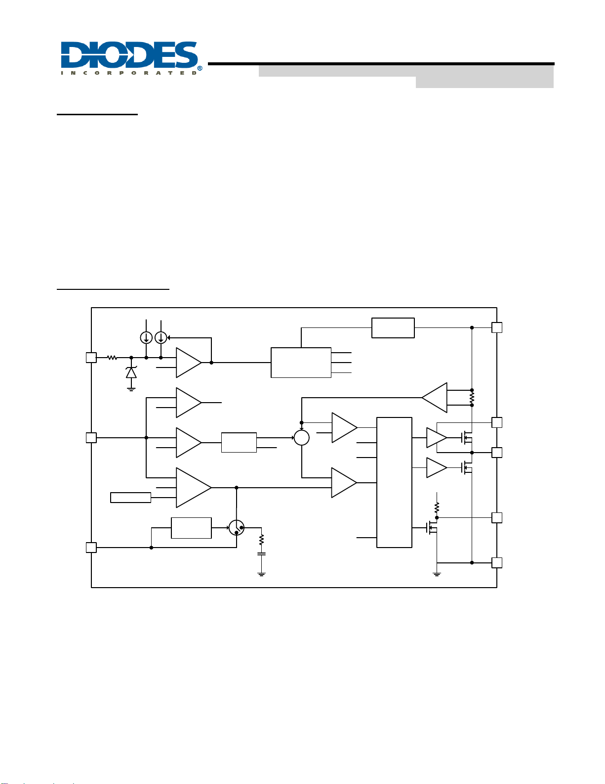
FUNCTIONAL BLOCK
0.88V
0.72V
OVP
Oscillator
450kHz
+
SE= 0.83V/T
RT= 0.2V/A
EN
FB
SW
VIN
Internal
Reference
VCC
Regulator
COMP
2ON
1.18V
I1
1.5μA
I2
4μA
20kΩ
1
0.4V
0.8V
1.1V
VCC
+
–
+
–
3+
–
+
+
–
gm
4
+
–
+
–
OSC
VSUM Control
Logic
GND
Detection
0.8V
Internal SS
Ref
18kΩ
7.6nF
PWM
Comparator
OCP
9
6
8
5MΩ
VCC
5
OSC
OVP
UVP
+
–
CSA
UVP
BST
PG
GND
Error
Amplifier
Figure 1. Functional Block Diagram
AP63356/7/Q-EVM
3.8V TO 32V INPUT, 3.5A LOW IQ SYNCHRONOUS BUCK WITH
ENHANCED EMI REDUCTION
AP63356Q/AP63357Q
Document number: DSxxxxRev. 1 - 1
3 of 11
www.diodes.com
August 2019
© Diodes Incorporated
ABSOLUTE MAXIMUM RATINGS
Symbol
Parameter
Rating
Unit
VIN
Supply Pin Voltage
-0.3 to +35.0 (DC)
V
-0.3 to +40.0 (400ms)
VEN
Enable/UVLO Pin Voltage
-0.3 to +35.0
V
VFB
Feedback Pin Voltage
-0.3 to +6.0
V
VCOMP
Compensation Pin Voltage
-0.3 to +6.0
V
VPG
Power-Good Pin Voltage
-0.3 to +6.0
V
VBST
Bootstrap Pin Voltage
VSW - 0.3 to VSW + 6.0
V
VSW
Switch Pin Voltage
-1.0 to VIN+ 0.3 (DC)
V
-2.5 to VIN + 2.0 (20ns)
TST
Storage Temperature
-65 to +150
°C
TJ
Junction Temperature
+170
°C
TL
Lead Temperature
+260
°C
ESD Susceptibility
HBM
Human Body Mode
2000
V
CDM
Charge Device Model
1000
V
RECOMMENDED OPERATING CONDITIONS
Symbol
Parameter
Min
Max
Unit
VIN
Supply Voltage
3.8
32
V
VOUT
Output Voltage
0.8
32
V
TA
Operating Ambient Temperature Range
-40
+125
°C
TJ
Operating Junction Temperature
Range
-40
+150
°C
AP63356/7/Q-EVM
3.8V TO 32V INPUT, 3.5A LOW IQ SYNCHRONOUS BUCK WITH
ENHANCED EMI REDUCTION
AP63356Q/AP63357Q
Document number: DSxxxxRev. 1 - 1
4 of 11
www.diodes.com
August 2019
© Diodes Incorporated
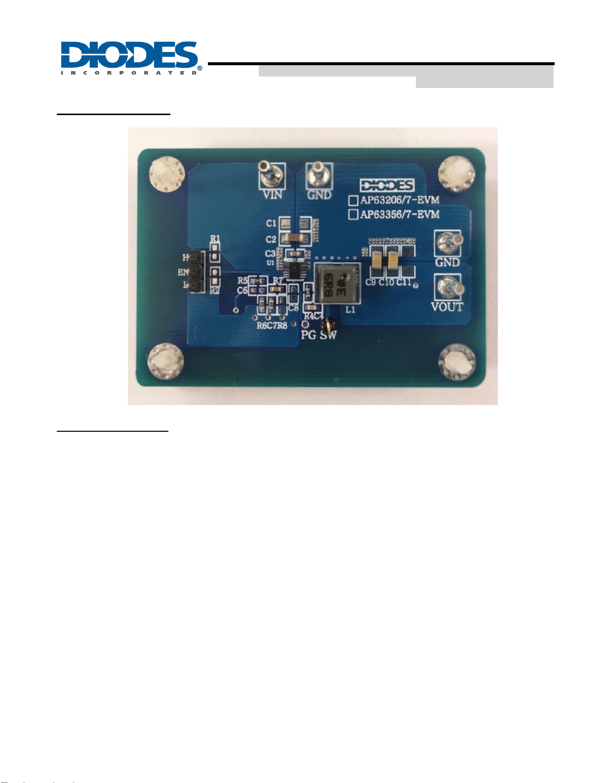
EVALUATION BOARD
QUICK START GUIDE
The AP63356/7/Q-EVM has a simple layout and allows access to the appropriate signals through test
points. To evaluate the performance of the AP63356/7/Q, follow the procedure below:
1. For evaluation board configured at VOUT=12V, connect a power supply to the input terminals VIN and
GND. Set VIN to 24V.
2. Connect the positive terminal of the electronic load to VOUT and negative terminal to GND.
3. For Enable, place a jumper to “H” position to enable IC. Jump to “L” position to disable IC.
4. The evaluation board should now power up with a 12V output voltage.
5. Check for the proper output voltage of 12V (±1%) at the output terminals VOUT and GND.
Measurement can also be done with a multimeter with the positive and negative leads between VOUT
and GND.
6. Set the load to 2A through the electronic load. Check for the stable operation of the SW signal on the
oscilloscope. Measure the switching frequency.

AP63356/7/Q-EVM
3.8V TO 32V INPUT, 3.5A LOW IQ SYNCHRONOUS BUCK WITH
ENHANCED EMI REDUCTION
AP63356Q/AP63357Q
Document number: DSxxxxRev. 1 - 1
5 of 11
www.diodes.com
August 2019
© Diodes Incorporated
MEASUREMENT/PERFORMANCE GUIDELINES:
1) When measuring the output voltage ripple, maintain the shortest possible ground lengths on the
oscilloscope probe. Long ground leads can erroneously inject high frequency noise into the
measured ripple.
2) For efficiency measurements, connect an ammeter in series with the input supply to measure the
input current. Connect an electronic load to the output for output current.
Setting the Output Voltage of AP63356/7
1) Setting the output voltage
The AP63356/7 features external programmable output voltage by using a resistor divider network R3
and R1 as shown in the typical application circuit. The output voltage is calculated as below,
6
65
8.0 RRR
VOUT
First, select a value for R1 according to the value recommended in the table 1. Then, R3 is determined.
The output voltage is given by Table 1 for reference. For accurate output voltage, 1% tolerance is
required. Table 1. Resistor selection for output voltage setting
Vo
R5
R6
C5(External/Internal
Compensation)
1.0V
7.45K
30K
NC
3.3V
93.5KΩ
30 KΩ
33pF/33pF
5.0V
157 KΩ
30 KΩ
NC/47pF
12V
420 KΩ
30 KΩ
NC
EXTERNAL COMPONENT SELECTION:
1) Input & output Capacitors (Cin, Cout)
(1) For lower output ripple, low ESR is required.
(2) Low leakage current needed, X5R/X7R ceramic recommend, multiple capacitor parallel
connection.
(3) The Cin and Cout capacitances are greater than 10uF and 44uF respective. When set output
voltage to 1.0V, 66uF Cout is recommended.
2) Bootstrap Voltage Regulator
(1) An external 0.1uF ceramic capacitor is required as bootstrap capacitor between BST and
SW pin to work as high side power MOSFET gate driver.
AP63356/7/Q-EVM
3.8V TO 32V INPUT, 3.5A LOW IQ SYNCHRONOUS BUCK WITH
ENHANCED EMI REDUCTION
AP63356Q/AP63357Q
Document number: DSxxxxRev. 1 - 1
6 of 11
www.diodes.com
August 2019
© Diodes Incorporated
3) Compensation Capacitors and Resistors
(1) For internal compensation: Connect Comp Pin to GND directly;
(2) For external compensation: A resistor and a capacitor in series are connected from Comp Pin
to GND, the value of resistor and capacitor is recommended refer to below table.
Output
capacitor(uF)
Vo=3.3V
Vo=5.0V
Vo=1.0V/12V
R7(KΩ)
C7(nF)
R7(KΩ)
C7(nF)
R7(Ω)
C7(nF)
44
25
3.3
24
3.3
Internal compensation Recommended
66
25
3.3
36
3.3
Internal compensation Recommended
4) Inductor (L)
(1) Low DCR for good efficiency
(2) Inductance saturate current must higher than the output current
(3) The recommended inductance is shown in the table 2 below.
Table 2. Recommended inductors
Output
Voltage
1.0V
3.3 V
5.0 V
12 V
Co=44uF
4.7uH
6.8uH
Co=66uF
2.2uH
6.8uH
6.8uH
10uH
Würth PART
744 393 460 47
744 393 460 68
744 393 440 22
744 393 460 68
744 393 460 68
744 393 461 00
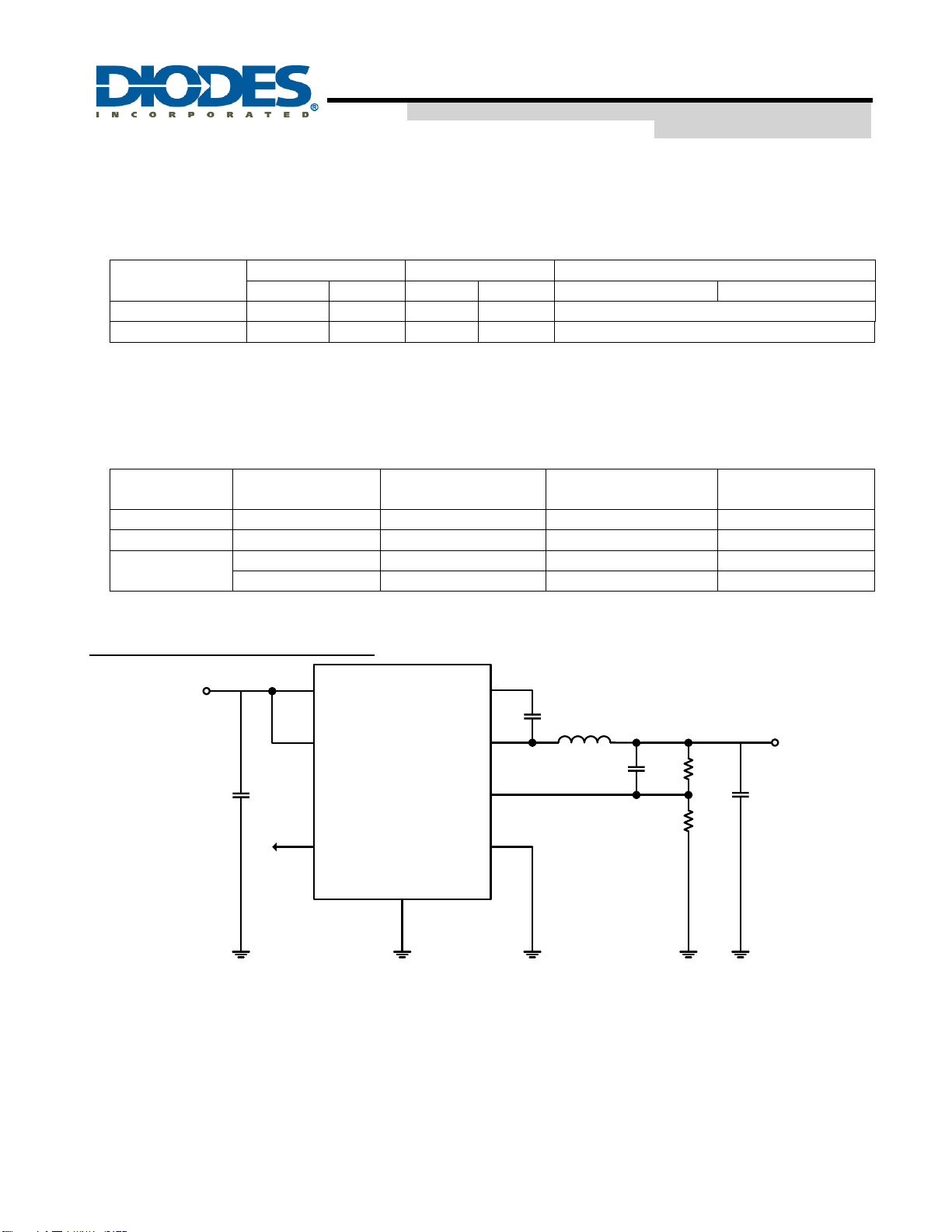
EVALUATION BOARD SCHEMATIC
AP63356Q
AP63357Q
1
VIN
2
EN
9
SW
6
BST
3
FB
8
GND
INPUT
R1
157kΩ
C4
47pF
R2
30kΩ
L
6.8μH
C3
100nF
C2
2x22µF
C1
10µF
OUTPUT VOUT
5V
5
PG
4
COMP
Figure 2. Typical Application Circuit
AP63356/7/Q-EVM
3.8V TO 32V INPUT, 3.5A LOW IQ SYNCHRONOUS BUCK WITH
ENHANCED EMI REDUCTION
AP63356Q/AP63357Q
Document number: DSxxxxRev. 1 - 1
7 of 11
www.diodes.com
August 2019
© Diodes Incorporated
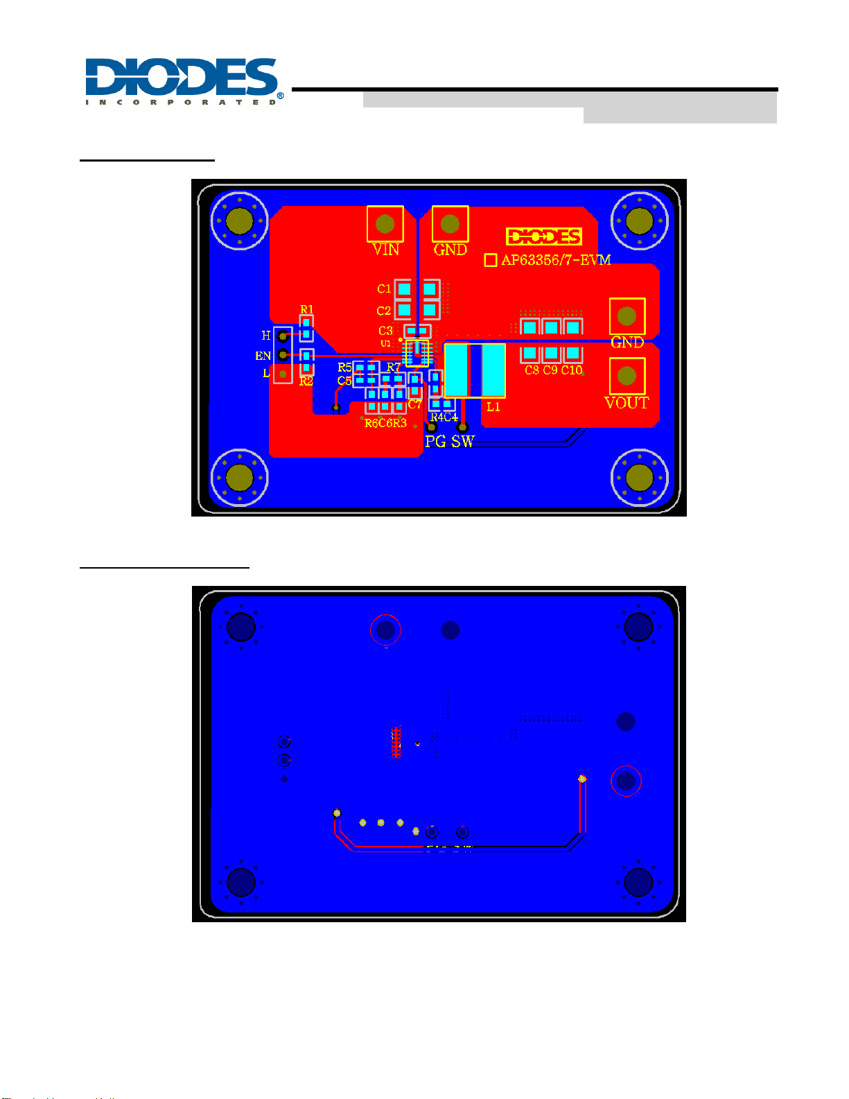
PCB TOP LAYOUT
Figure 3. AP63356/7/Q-EVM –Top Layer
PCB BOTTOM LAYOUT
Figure 4. AP63356/7/Q -EVM –Bottom Layer
AP63356/7/Q-EVM
3.8V TO 32V INPUT, 3.5A LOW IQ SYNCHRONOUS BUCK WITH
ENHANCED EMI REDUCTION
AP63356Q/AP63357Q
Document number: DSxxxxRev. 1 - 1
8 of 11
www.diodes.com
August 2019
© Diodes Incorporated
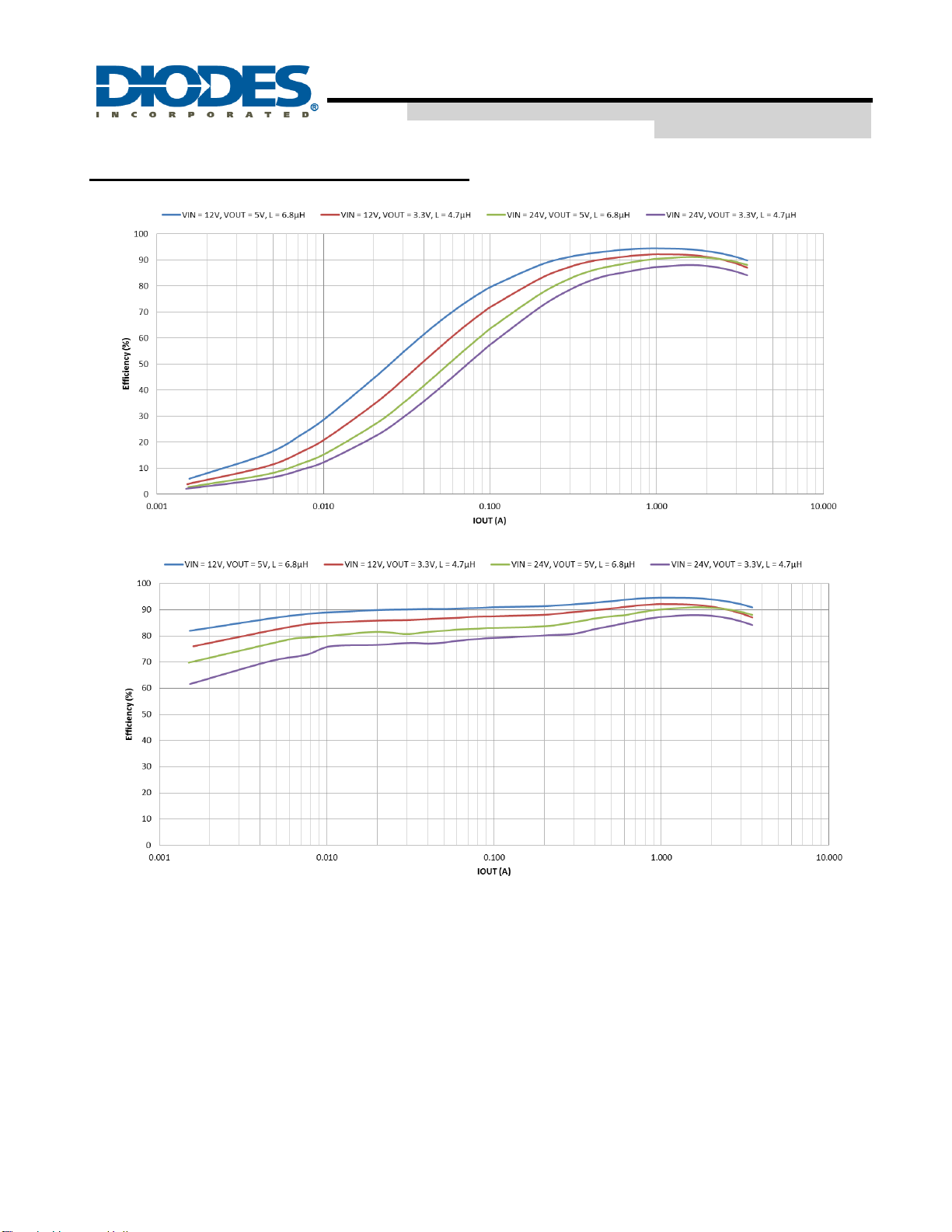
BILL OF MATERIALS for AP63356/7/Q-EVM (VOUT=12V)
Item
Value
Type
Rating
Description
C2
10uF
X5R/X7R, Ceramic/1206
35V
Input CAP
C3
0.1uF
X5R/X7R, Ceramic/0603
50V
Input CAP
C4
0.1uF
X5R/X7R, Ceramic/0603
50V
Bootstrap CAP
C7
3.3nF
X5R/X7R, Ceramic/0603
50V
Comp CAP
C9 & C10
22uF
X5R/X7R, Ceramic/1206
25V
Output CAP
L1
6.8uH
6060
5.0A
Inductor
R1
100K
0603
1%
Enable RES
R4
0
0603
1%
Bootstrap RES
R5
157K
0603
1%
Voltage set RES*
R6
30K
0603
1%
R7
36K
0603
1%
Comp RES
U1
AP63356/7
QFN
AP63356/7/Q-EVM
3.8V TO 32V INPUT, 3.5A LOW IQ SYNCHRONOUS BUCK WITH
ENHANCED EMI REDUCTION
AP63356Q/AP63357Q
Document number: DSxxxxRev. 1 - 1
9 of 11
www.diodes.com
August 2019
© Diodes Incorporated
TYPICAL PERFORMANCE CHARACTERISTICS
Figure 5. Efficiency vs. Output Current for AP63356Q
Figure 6. Efficiency vs. Output Current for AP63357Q
AP63356/7/Q-EVM
3.8V TO 32V INPUT, 3.5A LOW IQ SYNCHRONOUS BUCK WITH
ENHANCED EMI REDUCTION
AP63356Q/AP63357Q
Document number: DSxxxxRev. 1 - 1
10 of 11
www.diodes.com
August 2019
© Diodes Incorporated
Figure 7. AP63356 Output Voltage Ripple,
VIN = 12V, VOUT = 5V IOUT = 50mA
Figure 8. AP63357 Output Voltage Ripple,
VIN = 12V, VOUT = 5V IOUT = 50mA
Figure 9. AP63356/7 Output Voltage Ripple,
VIN = 12V, VOUT = 5V IOUT = 3.5A
VOUT (50mV/div)
IL(2A/div)
VSW (10V/div)
5μs/div
VOUT (50mV/div)
IL(1A/div)
VSW (10V/div)
50μs/div
5μs/div
VOUT (50mV/div)
IL(2A/div)
VSW (10V/div)

AP63356/7/Q-EVM
3.8V TO 32V INPUT, 3.5A LOW IQ SYNCHRONOUS BUCK WITH
ENHANCED EMI REDUCTION
AP63356Q/AP63357Q
Document number: DSxxxxRev. 1 - 1
11 of 11
www.diodes.com
August 2019
© Diodes Incorporated
IMPORTANT NOTICE
DIODES INCORPORATED MAKES NO WARRANTY OF ANY KIND, EXPRESS OR IMPLIED, WITH REGARDS TO THIS DOCUMENT,
INCLUDING, BUT NOT LIMITED TO, THE IMPLIED WARRANTIES OF MERCHANTABILITY AND FITNESS FOR A PARTICULAR PURPOSE
(AND THEIR EQUIVALENTS UNDER THE LAWS OF ANY JURISDICTION).
Diodes Incorporated and its subsidiaries reserve the right to make modifications, enhancements, improvements, corrections or other changes
without further notice to this document and any product described herein. Diodes Incorporated does not assume any liability arising out of the
application or use of this document or any product described herein; neither does Diodes Incorporated convey any license under its patent or
trademark rights, nor the rights of others. Any Customer or user of this document or products described herein in such applications shall assume
all risks of such use and will agree to hold Diodes Incorporated and all the companies whose products are represented on Diodes Incorporated
website, harmless against all damages.
Diodes Incorporated does not warrant or accept any liability whatsoever in respect of any products purchased through unauthorized sales channel.
Should Customers purchase or use Diodes Incorporated products for any unintended or unauthorized application, Customers shall indemnify and
hold Diodes Incorporated and its representatives harmless against all claims, damages, expenses, and attorney fees arising out of, directly or
indirectly, any claim of personal injury or death associated with such unintended or unauthorized application.
Products described herein may be covered by one or more United States, international or foreign patents pending. Product names and markings
noted herein may also be covered by one or more United States, international or foreign trademarks.
This document is written in English but may be translated into multiple languages for reference. Only the English version of this document is the
final and determinative format released by Diodes Incorporated.
LIFE SUPPORT
Diodes Incorporated products are specifically not authorized for use as critical components in life support devices or systems without the express
written approval of the Chief Executive Officer of Diodes Incorporated. As used herein:
A. Life support devices or systems are devices or systems which:
1. are intended to implant into the body, or
2. support or sustain life and whose failure to perform when properly used in accordance with instructions for use provided in the
labeling can be reasonably expected to result in significant injury to the user.
B. A critical component is any component in a life support device or system whose failure to perform can be reasonably expected to cause the
failure of the life support device or to affect its safety or effectiveness.
Customers represent that they have all necessary expertise in the safety and regulatory ramifications of their life support devices or systems, and
acknowledge and agree that they are solely responsible for all legal, regulatory and safety-related requirements concerning their products and any
use of Diodes Incorporated products in such safety-critical, life support devices or systems, notwithstanding any devices- or systems-related
information or support that may be provided by Diodes Incorporated. Further, Customers must fully indemnify Diodes Incorporated and its
representatives against any damages arising out of the use of Diodes Incorporated products in such safety-critical, life support devices or systems.
Copyright © 2019, Diodes Incorporated
www.diodes.com
This manual suits for next models
1
Table of contents
Other Diodes Motherboard manuals

Diodes
Diodes AL8400QEV1 User manual

Diodes
Diodes EV1 User manual

Diodes
Diodes PI6CG18801 Mounting instructions

Diodes
Diodes ZXLD1374QEV1 User manual

Diodes
Diodes ZXLD1370 EV4 User manual

Diodes
Diodes AP63300-EVM User manual

Diodes
Diodes AL5802EV1 User manual

Diodes
Diodes AP3983R User manual

Diodes
Diodes AP3041EV1 User manual

Diodes
Diodes AP3981D2 User manual


