Diodes ZXLD1374QEV1 User manual
September 2018 www.diodes.com
© Diodes Incorporated, 2018
ZXLD1374QEV1 BUCK LED DRIVER
USER GUIDE
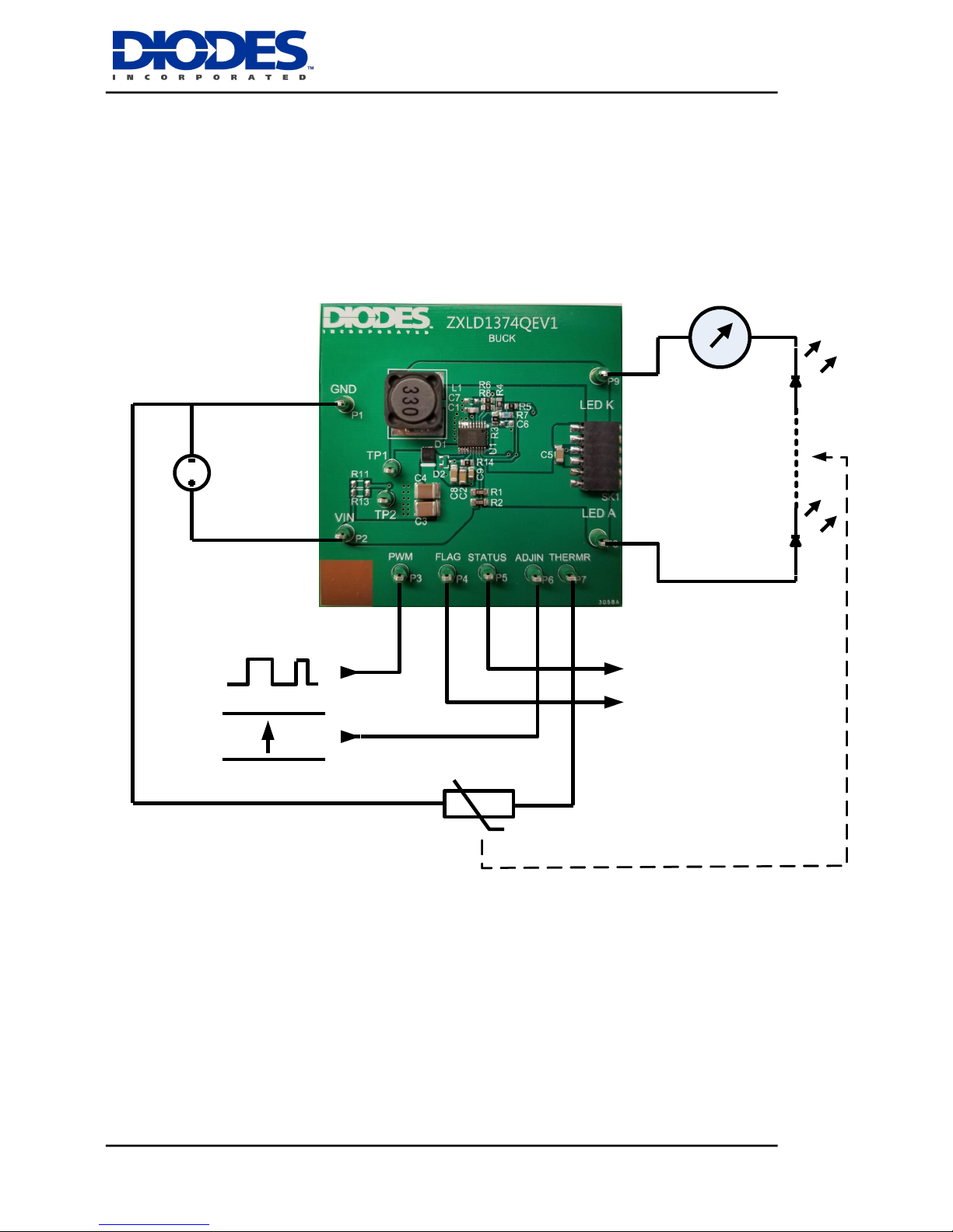
Fig. 1 ZXLD1374QEV1 Evaluation board connection diagram
8-48V 2A
DC PSU
0-1.5A DC
DVM
1 - 15 LEDs
1.5A
0V
4.5V
Open Drain output
125mV = 10%
2.5V = 200%
-t°
GND
0 –4.5V Status steps
Thermal connection
ZXLD1374QEV1
September 2018 www.diodes.com
© Diodes Incorporated 2018 2
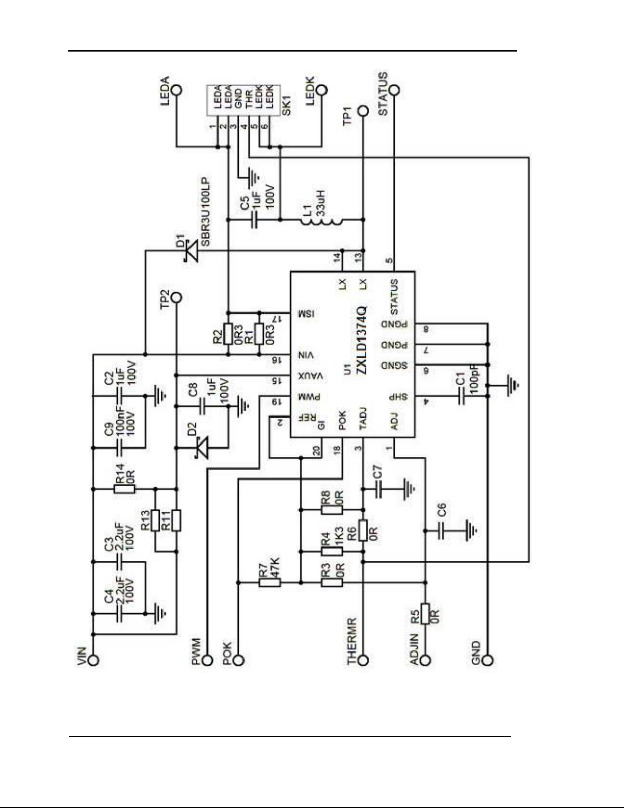
Fig. 2 ZXLD1374QEV1 Schematic Diagram
ZXLD1374QEV1
September 2018 www.diodes.com
© Diodes Incorporated 2018 3
PARTS LIST
Ref
Value
Package
Part Number
Manufacturer
Contact Details
U1
1.5A LED Driver
TSSOP20L- EP
ZXLD1374Q
Diodes
www.diodes.com
D1
Freewheeling
diode 3A 100V
DFN3030
SBR3U100LP
Diodes
www.diodes.com
D2
NOT FITTED
SOT23
DDZX15
Diodes
www.diodes.com
L1
33uH 2.3A
MSS1278-333MLB
NPIS27H330MTRF
744-770-133
Coilcraft
NIC Comps.
Wurth
www.coilcraft.com
www.niccomp.com
www.we-
online.com
C1
100pF 10V
0805
generic
C2 C5
C8
1uF 100V X7R
1206
GRM31CR72A105
KA01L
Murata /
generic
www.murata.com
C3 C4
2.2uF 100V X7R
1812
GRM43ER72A225
KA01L
Murata /
generic
www.murata.com
C6 C7
NOT FITTED
C9
100nF 100V X7R
0805
generic
R1 R2
0R3
1206
generic
R3 R5
R6 R8
R14
0R
0805
generic
R4
1K3
0805
generic
R7
47K
0805
generic
R11,
R13
NOT FITTED
1206
NOTES
The PCB is supplied with R3 and R8 0R0 resistors fitted.
The ‘ADJ’pin and the ‘TADJ’pin are disabled.
‘VIN’and ‘VAUX’are shorted on ZXLD1374QEV1
The LED current of the ZXLD1374QEV1 boards = 1.5A with 2x // 0R3 = 0R15 (R1 & R2)
The ZXLD1374Q ‘VAUX’pin can be driven from a separate supply instead of the ‘VIN’voltage.
To do this, remove R14, fit R11 = 10k0, fit R13 = 10k0.
Use Zener diode D2 to keep ‘VAUX’pin <15V.
For other reference designs or more applications information, please see the ZXLD1374Q datasheet.
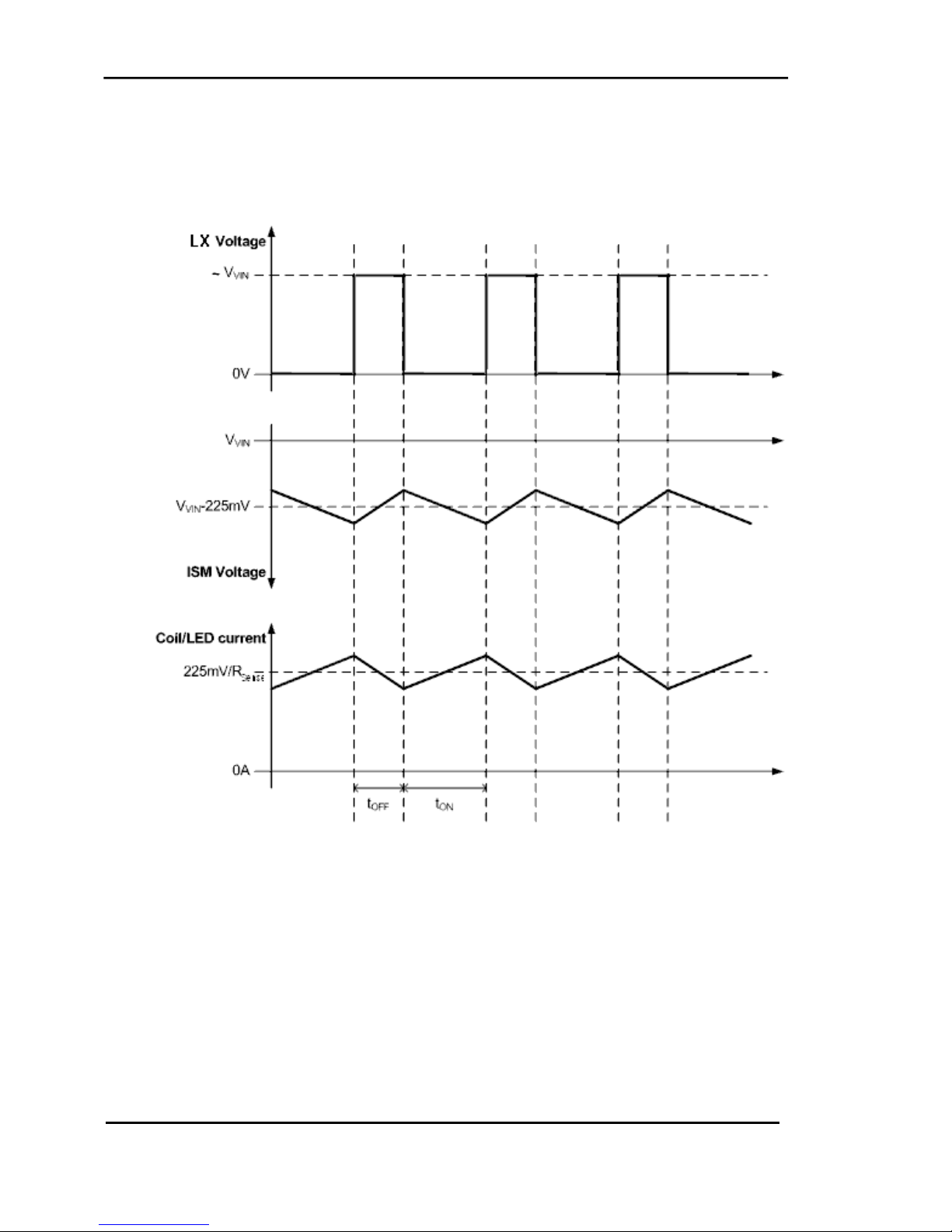
OPERATION
In Buck mode the LED current is sensed by the series resistor (R1 // R2). An output from the control loop
responsible for sensing this current drives the input of an internal comparator. The comparator then drives the
gate of the internal NMOS switch transistor. When the NMOS switch is on (LX pin low), current flows from VIN,
via (R1 // R2), inductor and switch to ground and increases until a high value is reached. Then, the switch
turns off (LX pin high) and the current flows through (R1 // R2), the inductor, the LED and D1, to ‘VIN’. When
the inductor current has gone low, ‘LX’ goes low, the cycle of events repeats and so the circuit oscillates. The
average current in the LEDs is equal to the average of the maximum and minimum threshold currents. The
ripple current (hysteresis) is equal to the difference between the thresholds. The average current in the LED is
equal to the average current in the inductor. The control loop keeps the average LED current at the level set
by the voltage on the ‘ADJ’pin. Loop compensation is achieved by C1.
ZXLD1374QEV1
September 2018 www.diodes.com
© Diodes Incorporated 2018 4
Fig. 3 Waveforms
ZXLD1374QEV1
September 2018 www.diodes.com
© Diodes Incorporated 2018 5
ADJ Terminal (DC output current adjustment)
On the ZXLD1374QEV1, R3 connects the ‘ADJ’pin to ‘VREF’to give 100% LED current.
The ‘ADJ’pin can be driven with an external DC voltage >=125mV and <=2.5V to adjust the LED current to
>=10% and <=200% of the nominal value.
To do this, remove R3, fit R5 and apply an external DC voltage between ‘ADJIN’and ‘GND’.
The voltage ‘VADJ ‘can be derived from a resistor-divider connected between ‘REF’and ‘GND’.
‘ADJ’has a high impedance within its normal operating voltage range. An internal 2.6V clamp protects the
device against high input voltages and limits the maximum output current to about 4% above the maximum
current set by ‘VADJ ‘ if the maximum input voltage is exceeded.
PWM Terminal (PWM output current control/dimming)
The LED current can be adjusted digitally, by applying a low frequency PWM logic signal to the ‘PWM’pin to
turn the controller on and off. This will produce an average output current proportional to the duty cycle of the
control signal. During PWM operation, the device remains powered-up and only the output is switched by the
control signal.
The device can be shut down by taking the ‘PWM’ pin to < 0.4V for >15ms, with a short to 0V or suitable open
collector NPN, or open drain NMOS transistor. In shutdown, most of the circuitry inside the device is turned off
and the quiescent current will be typically 90µA.
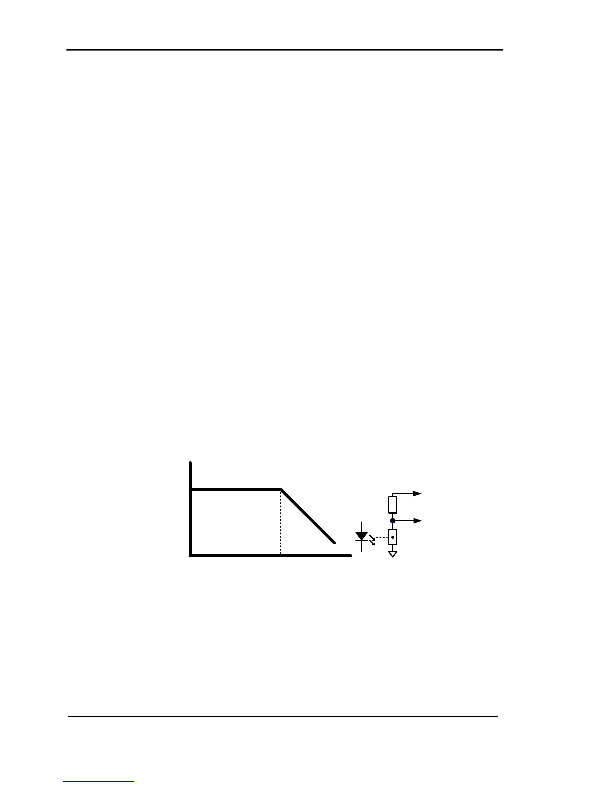
TADJ Terminal (Thermal control of LED current)
The Thermal control circuit monitors the voltage on the ‘TADJ’pin and reduces the output current linearly if the
voltage on ‘TADJ’< 625mV. An NTC thermistor and resistor can be connected to set the voltage on the ‘TADJ’
pin = 625mV at the required threshold temperature. This will give 100% LED current below the threshold
temperature and <100% current above it as shown in the graph. The temperature threshold can be changed
by adjusting the value of Rth and/or the thermistor to suit the LED used.
On the ZXLD1374QEV1, Rth is 1K3 (R4). To use Thermal control, remove R8, fit R6, and fit a 10K NTC
(Negative Temperature Coefficient) type thermistor between ‘TADJ’and ‘GND’. This will set the threshold
temperature to ~90ºC.
Thermal control by LED current reduction
100%
ILED
LED Temperature
T threshold
Set by R th
REF
TADJ
LED
R th
Th 1
Fig. 4 Thermal control
The Thermal Control feature can be disabled by connecting ‘TADJ’to ‘REF’through the jumper resistor R8.
ZXLD1374QEV1
September 2018 www.diodes.com
© Diodes Incorporated 2018 6
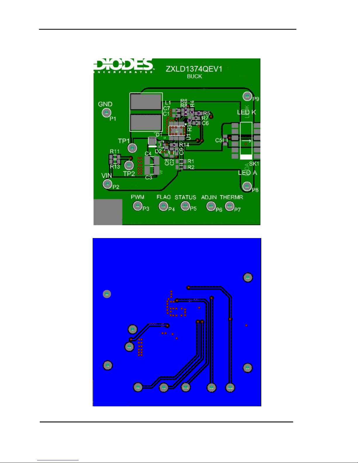
BOARD LAYOUT

ZXLD1374QEV1
September 2018 www.diodes.com
© Diodes Incorporated 2018 7
IMPORTANT NOTICE
DIODES INCORPORATED MAKES NO WARRANTY OF ANY KIND, EXPRESS OR IMPLIED, WITH REGARD TO THIS
DOCUMENT, INCLUDING, BUT NOT LIMITED TO, THE IMPLIED WARRANTIES OF MERCHANTABILITY AND
FITNESS FOR A PARTICULAR PURPOSE (AND THEIR EQUIVALENTS UNDER THE LAWS OF ANY JURISDICTION).
Diodes Incorporated and its subsidiaries reserve the right to make modifications, enhancements, improvements,
corrections or other changes without further notice to this document and any product described herein. Diodes Incorporated
does not assume any liability arising out of the application or use of this document or any product described herein; neither
does Diodes Incorporated convey any license under its patent or trademark rights, nor the rights of others. Any Customer
or user of this document or products described herein in such applications shall assume all risks of such use and will agree
to hold Diodes Incorporated and all the companies whose products are represented on Diodes Incorporated website,
harmless against all damages.
Diodes Incorporated does not warrant or accept any liability whatsoever in respect of any products purchased through
unauthorized sales channels. Should Customers purchase or use Diodes Incorporated products for any unintended or
unauthorized application, Customers shall indemnify and hold Diodes Incorporated and its representatives harmless
against all claims, damages, expenses, and attorney fees arising out of, directly or indirectly, any claim of personal injury or
death associated with such unintended or unauthorized application.
Products described herein may be covered by one or more United States, international or foreign patents pending. Product
names and markings noted herein may also be covered by one or more United States, international or foreign trademarks.
LIFE SUPPORT
Diodes Incorporated products are specifically not authorized for use as critical components in life support devices or
systems without the express written approval of the Chief Executive Officer of Diodes Incorporated. As used herein:
A. Life support devices or systems are devices or systems which:
1. are intended to implant into the body, or
2. support or sustain life and whose failure to perform when properly used in accordance with instructions for use
provided in the labeling can be reasonably expected to result in significant injury to the user.
B. A critical component is any component in a life support device or system whose failure to perform can be reasonably
be expected to cause the failure of the life support device or to affect its safety or effectiveness.
Customers represent that they have all necessary expertise in the safety and regulatory ramifications of their life support
devices or systems, and acknowledge and agree that they are solely responsible for all legal, regulatory and safety-related
requirements concerning their products and any use of Diodes Incorporated products in such safety-critical, life support
devices or systems, notwithstanding any devices- or systems-related information or support that may be provided by
Diodes Incorporated. Further, Customers must fully indemnify Diodes Incorporated and its representatives against any
damages arising out of the use of Diodes Incorporated products in such safety-critical, life support devices or systems.
Copyright © 2018, Diodes Incorporated
www.diodes.com
Table of contents
Other Diodes Motherboard manuals

Diodes
Diodes AP3983R User manual

Diodes
Diodes AP63300-EVM User manual

Diodes
Diodes AL8400QEV1 User manual

Diodes
Diodes AP3981D2 User manual

Diodes
Diodes ZXLD1370 EV4 User manual

Diodes
Diodes AP3981B User manual

Diodes
Diodes AL5802EV1 User manual

Diodes
Diodes PI6CG18801 Mounting instructions

Diodes
Diodes AP3041EV1 User manual

Diodes
Diodes AP63356Q-EVM User manual


