Diodes EV1 User manual

45W USB PD 3.0 Adaptor EV1 Board User Guide
45W USB PD 3.0 AP3108L+APR346+CY2311 Page 1 of 28 7-1-2018
Release 1.0 www.diodes.com
Table of Contents
Chapter 1. Summary_________________________ 2
1.1 General Description _______________________ 2
1.2 Key Features _____________________________ 2
1.2.1 System Key Features_________________________ 2
1.2.2 AP3108L Key Features _______________________ 2
1.2.3 APR346 Key Features ________________________ 2
1.2.4 CY2311_16L Key Feature _____________________ 2
1.3 Applications______________________________ 2
1.4 Main Power Specifications (CV & CC Mode) ____ 2
1.5 Evaluation Board Picture ___________________ 2
Chapter 2. Power Supply Specification__________ 3
2.1 Specification and Test Results _______________ 3
2.2 Compliance ______________________________ 3
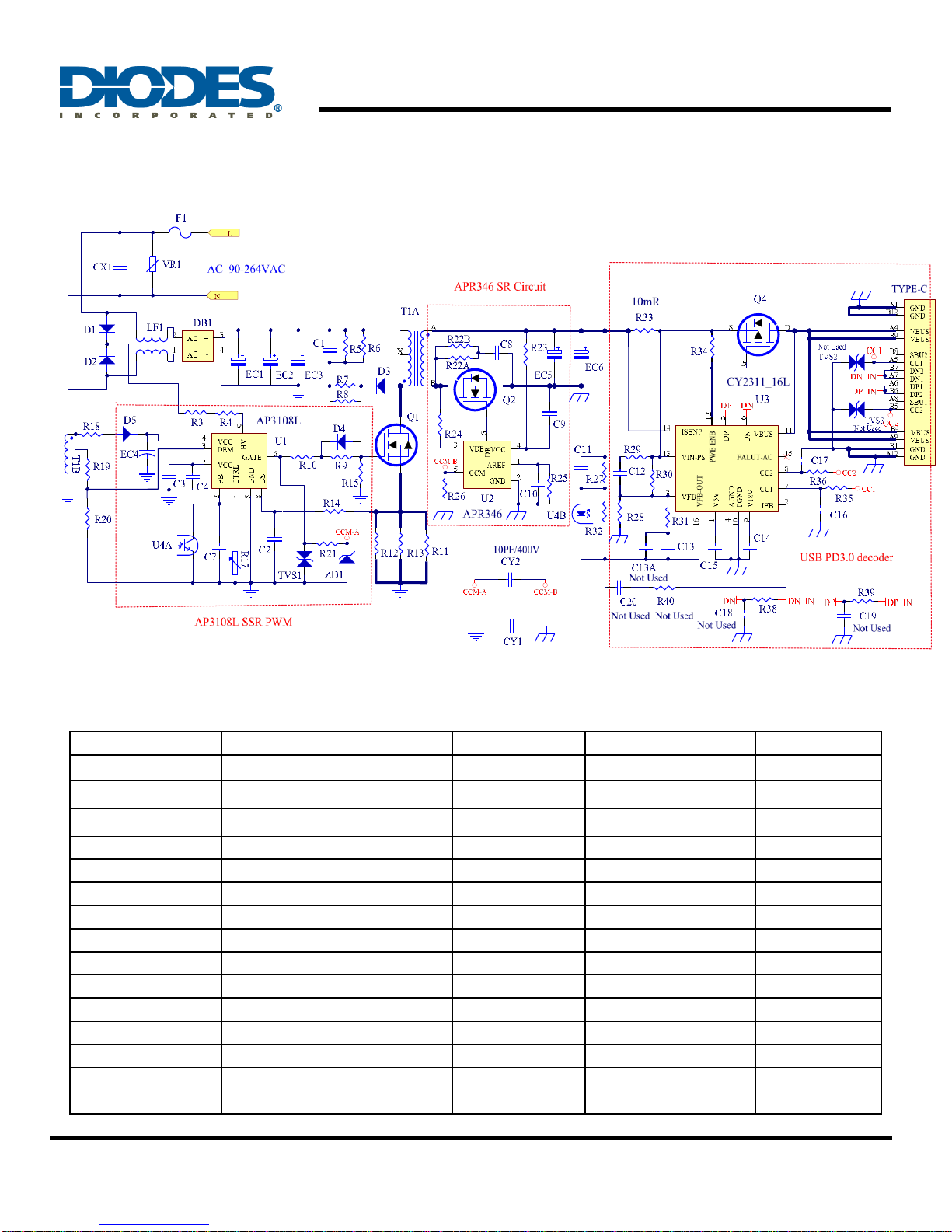
Chapter 3. Schematic ________________________ 4
3.1 EV1 Board Schematic ______________________ 4
3.2 Bill of Material (BOM)______________________ 4
3.3 Transformer Design Specification ____________ 6
3.4 Schematics Description_____________________ 7
3.4.1 AC Input Circuit & Differential Filter ____________ 7
3.4.2 AP3108L PWM Controller_____________________ 7
3.4.3 APR346 Synchronous Rectification (SR) MOSFET
Driver _________________________________________ 7
3.4.4 CY2311_16L PD3.0+ Decoder & Protection on /off P
MOSFET and Interface to Power Devices _____________ 7
Chapter 4. The Evaluation Board (EVB) Connections8
4.1 EVB PCB Layout ___________________________ 8
4.2 Quick Start Guide Before Connection _________ 8
4.3 System Setup_____________________________ 9
4.3.1 Connection with E-Load ______________________ 9
4.3.2 Canyon –Quick Charge 4/4+ Test Kit ___________10
4.3.3 Input & Output Wires Connection _____________ 10
Chapter 5. Testing the Evaluation Board________ 11
5.1 Input & Output Characteristics______________ 11
5.1.1 Input Standby Power _______________________11
5.1.2 Input Power Efficiency at Different AC Line Input
Voltage _______________________________________ 11
5.1.3 Average Efficiency at Different Loading ( @ PCB end)
_____________________________________________12
5.2 Key Performance Waveforms _______________ 12
5.2.1 45W PD3.0 System Start-up Time & Hold-up Time 12
5.2.2 Q1 /Q2 Main Switching Voltage MOSFET Stress on at
20V/ 2.25A Loading @264Vac ____________________ 13
5.2.3 System Output Ripple & Noise with @ PCB End _ 13
5.2.4 Dynamic load ----0A-3A 10mS 125mA/uS( PCB End)
_____________________________________________ 17
5.2.5 Output Voltage Transition Time ______________ 19
5.2.6 Output Voltage Transition Time from High to Low 21
5.2.7 Thermal Testing ___________________________ 22

45W USB PD 3.0 Adaptor EV1 Board User Guide
45W USB PD 3.0 AP3108L+APR346+CY2311 Page 2 of 28 7-1-2018
Release 1.0 www.diodes.com
Chapter 1. Summary
1.1 General Description
The 45W USB PD 3.0 Adaptor Evaluation Board EV1 is
composed of three main parts, AP3108L offers the DCM/CCM
PWM switching, APR346 is a Synchronous Rectification
Controller, and the CY2311_16L is USB 3.0 protocol decoder.
Based on monitoring CC1 & CC2 signals, CY2311_16L interprets
desired voltage and current setting, and then feedback
information to primary side AP3108L controller for providing well
regulated voltage and current as well as related power
protections.
1.2 Key Features
1.2.1 System Key Features
SSR Topology Implementation with an Opto-coupler for
Accurate Step Voltage Controlling
USB PD 3.0 Compliance
Meet DOE 6 and CoC Tier 2 Efficiency Requirements
<30mW No-Load Standby Power
1.2.2 AP3108L Key Features
Current Mode PWM Controller
Frequency Shift function changes frequency per line loading
Frequency fold back for high average efficiency
Integration of High-Voltage Start-Up Circuit to enable low
standby power
Integration of 100V LDO, X-Cap discharge for minimal
system BOM components
Constant load output current during output short circuit
Rich Protection Functions: , Precise Secondary Side OVP,
UVP, OLP, BNO, FOCP, SSCP, External Programmable
OTP
1.2.3 APR346 Key Features
Synchronous Rectification operating at DCM, CCM and QR
mode for Flyback topology
Eliminate Resonant Ringing Interference
Fewest External Components used
1.2.4 CY2311_16L Key Features
Type-C USB PD DFP (Downstream Facing Port)
USB PD2.0, PD 3.0 Protocol Decoding
10-Bit ADCs for voltage and current monitoring
Built in Shunt Regulator for Constant Voltage and Constant
Current
Programmable OVP/UVP/OCP/OTP
Internal Discharge MOS
Internal Vbus Load Switch Driver
3V- 30V Operation Voltage without External Regulator
Package 16-Pin TSSOP
USB PD IC Compliance Certified –TID #1060013,
12/18/2017 (http://canyon-semi.com.tw/images/USB-
IF_compliance_certification1211.pdf)
1.3 Applications
USB PD 3.0 Wall Adaptor
USB PD 3.0 Car Charger
1.4 Main Power Specifications (CV & CC Mode)
Parameter
Value
Input Voltage
90Vac to 264Vac
Input standby power
< 30mW
Main Output
Vo / Io
5V/3A, 9V/3A, 12V/3A,
15V/3A, 20V/2.25A
Efficiency
89%
Total Output Power
45W
Protections
OVP, UVP, OLP, BNO, FOCP,
SSCP, OTP
XYZ Dimension
67 x 41 x 25mm
ROHS Compliance
Yes
1.5 Evaluation Board Picture
Figure 1: Top View
Figure 2: Bottom View

45W USB PD 3.0 Adaptor EV1 Board User Guide
45W USB PD 3.0 AP3108L+APR346+CY2311 Page 3 of 28 7-1-2018
Release 1.0 www.diodes.com
Chapter 2. Power Supply Specification
2.1 Specification and Test Results
2.2 Compliance
Parameter
Test conditions
Low to High
High to Low
standard
Test Summary
Standby Power (mW)
5V Output / @230Vac
-
24mW
30mW
Pass
Output Voltage Transition time
5V/3A to 9V/3A
49ms
50ms
275mS <
Pass
Output Voltage Transition time
9V/3A to 12V/3A
41ms
39ms
275mS <
Pass
Output Voltage Transition time
12V/3A to 15V3A
41ms
39ms
275ms <
Pass
Output Voltage Transition time
15V/3A to 20V/2.25A
65ms
76ms
275mS <
Pass
Output Voltage Transition time
5V/3A to 20V/2,25A
211ms
249ms
275mS <
Pass
Output Connector
USB Type C
-
-
-
Temperature
90Vac , 15V / 3A
-
-
-
Pass
Dimensions (W /D/ H)
L67mm x 41mm x 25mm
-
-
-
Safety
IEC/EN/UL 60950 Standard
-
-
-
EMI Conduction
FCC/EN55022 Class B
-
-
-
Pass
Parameter Testconditions Min Nom Max Eff / DoE
VI Eff /
Tier2 TestSummary
Vacin Input Voltage 90 Vrms 115/230 264Vrms
Fline Frequency 47 Hz 50/60 64 Hz
Iin Input Current 1.3Arms Pass
No load Pin At 230Vac_in/50Hz,
@5V, Pin < 75mW 30mW Pass, the test result is 24mW
5V/3A @115Vac/230Vac
Averageefficiency Board end 5V/3A 81.39% 81.84% Pass,average efficiencyis86.93%
5V/3A @115Vac/230Vac
10% efficiency Board end 5V/0.3A 72.48% Pass,efficiencyis 82.04%
9V/3A @115Vac/230Vac
Averageefficiency Board end 9V/3A 86.60% 87.30% Pass,averageefficiencyis89.37%
9V/3A @115Vac/230Vac
10% efficiency Board end 9V/0.3A 76.62% Pass,efficiencyis 80.86%
12V/3A @115Vac/230Vac
Averageefficiency Boardend 12V/3A 87.4% 88.3% Pass,averageefficiencyis89.91%
12V/3A @115Vac/230Vac
10% efficiency Board end 12V/0.3A 77.4% Pass,efficiencyis 82.72%
15V/3A @115Vac/230Vac
10% efficiency Board end 15V/3A 87.7% 88.8% Pass,averageefficiencyis90.03%
15V/3A @115Vac/230Vac
10% efficiency Board end 15V/0.3A 78.85% Pass,efficiencyis 83.78%
20V/2.25A
@115Vac/230Vac
10% efficiency
Board end 20V/2.25A 87.7% 88.8% Pass,averageefficiencyis89.18%
20V/2.25A
@115Vac/230Vac
10% efficiency
Board end 20V/0.225A 78.85% Pass,efficiencyis 80.48%
45W USB PD 3.0 Adaptor EV1 Board User Guide
45W USB PD 3.0 AP3108L+APR346+CY2311 Page 4 of 28 7-1-2018
Release 1.0 www.diodes.com
Chapter 3. Schematic
3.1 EV1 Board Schematic
Figure 3: Evaluation Board Schematic
3.2 Bill of Material (BOM)
Designator
Description
Manufactory
Footprint
Quantity
C1
1nF/1KV
C1206
1
C2
220pF/25V
C0603
1
C3, C4
4.7uF/50V
C0805
2
C7
1.2nF/50V
C0603
1
C8
2.2nF/200V
C0805
1
C9
100nF/50V
C0603
1
C10
15nF/25V
C0603
1
C11, C12
1nF/50V
C0603
2
C13
68nF/50V
C0603
1
C14
100nF/25V
C0603
1
C15
4.7uF/7.5V
C0805
1
C16, C17
220pF/25V
C0603
2
C13A
Not Used
C0603
C20
Not Used
C0603
C18,C19
Not Used
C0603
45W USB PD 3.0 Adaptor EV1 Board User Guide
45W USB PD 3.0 AP3108L+APR346+CY2311 Page 5 of 28 7-1-2018
Release 1.0 www.diodes.com
CX1
330nF/275VAC, X-CAP
1
CY1
1nF/400V, Y-CAP
CY-10.0
1
CY2
10PF/400V, Y-CAP
CY-10.0
1
EC1
22UF/400V,E-CAP
1
EC2, EC3
27UF/400V,E-CAP
2
EC4
22uF/100V,E-CAP
1
EC5
680UF/25V,Solid Cap
1
EC6
680UF/25V, E-Cap
1
T1
T-RM10, Lp=760uH
RM10
1
VR1
Varistor, '561
1
F1
T3.15A/250V
1
J1
USB TYPE-C Connector
C-TYPE-C
1
LF1
Common Chock, Lp > 20mH
1
R3, R4
10K,1206
R1206
2
R5, R6
390K,1206
R1206
2
R7, R8
33R,1206
R1206
2
R9
82R
R0603
1
R10
10R
R0603
1
R11, R12, R13
1.0R
R1206
3
R14, R29
1K
R0603
2
R15
22K
R0603
1
R17
100K NTC
R0603
1
R18
2.2R
R0805
1
R19
270K
R0603
1
R20
20K
R0603
1
R21
2K
R1206
1
R22A, R22B
47R
R0805
2
R23, R24, R35,
R36,R38,R39
20R
R0603
6
R25, R30
91K
R0603
2
R26
3K
R0603
1
R27
3K
R1206
1
R28
10K
R0603
1
R31, R32
4.7K
R0603
2
R33
Current sense resistor, 10mR
R1206
1
R34
47K
R0603
1
R40
Not Used
R0603
D1, D2, D5
S1MWF
DIODES
SOD-123
3
D3
S3MB
DIODES
SMB
1
D4
1N4148WS
DIODES
SOD-323
1
DB1
TT410
DIODES
MSBL
1
TVS1
DESD1LIN2WSQ
DIODES
SOD-323
1
45W USB PD 3.0 Adaptor EV1 Board User Guide
45W USB PD 3.0 AP3108L+APR346+CY2311 Page 6 of 28 7-1-2018
Release 1.0 www.diodes.com
3.3 Transformer Design Specification
RM10(Ae=98mm2)
NO
NAME
TERMINAL NO.
WINDING
START
FINISH
WIRE
TURNS
Layers
1
Np1
1(Add Tube)
X
Φ 0.37*2
35
3
2
Na
10(Add Tube)
3(GND)
Φ 0.25*2
17
1
3
Shield1
3
NC
Φ 0.14*1
7
1
4
Ns1
A
B
Φ 0.8TIW *1
(Triple Insulated Wire)
7
1
5
Shield2
3
NC
Φ 0.14*1
30
1
6
Np2
X
12
Φ 0.37*2
11
1
Primary Inductance
Pin 1-12,all other windings open, measured at 20kHz, 0.4VRMS
760uH±5%
Primary Leakage
Inductance
Pin 1-12, all other windings shorted, measured at 20kHz, 0.4VRMS
20 uH (Max.)
Note
1,Core connect to Pin3
2,Core:PC40
TVS2, TVS3
Optional
SOD-323
U1
AP3108L
DIODES
SSOP-9
1
U2
APR346
DIODES
SOT23-6
1
U3
CY2311_16L
DIODES
SSOP-16
1
ZD1
MMSZ5248B
DIODES
SOD-123
1
Q1
DMJ65H600SCTI
DIODES
TO-220
1
Q2
DMT10H010LPS-13
DIODES
POWERDI5060-8
1
Q4
DMP3007SCG
DIODES
DFN3*3
1
U4
Opto coupler, TCLT1006
1

45W USB PD 3.0 Adaptor EV1 Board User Guide
45W USB PD 3.0 AP3108L+APR346+CY2311 Page 7 of 28 7-1-2018
Release 1.0 www.diodes.com
3.4 Schematics Description
3.4.1 AC Input Circuit & Differential Filter
There are three components in the section. The Fuse F1 protects against over-current conditions which occur when some main
components failed. The LF1 & CX1 are common mode chock filter for the common mode noise suppression filleting because of the
each coil with large impedance. The DB1 is rectifier, and basically converts alternating current & voltage into direct current & voltage.
3.4.2 AP3108L PWM Controller
The AP3108L PWM controller U1 and Opto-Coupler U4 and Q1 are the power converting core components. Connected to filtered
output after bridge circuit, R3 & R4 resistor path will provide start-up voltage and current during starting up through HV (Pin 9).
Subsequent VCC power will be provided by voltage feedback from the auxiliary winding through R18-D5. This design is to
accommodate with the required wide voltage range to support various protocols (including USB PD Programmable Power Supply
PPS), from 5V to 20V.
Based on feedback of secondary side (Pin CATH of CY2311_16L Decoder) to primary side (FB pin of AP3108L) through Opto-
coupler U4, AP3108L will switch ON and Off Q1 to regulate desired voltage and current on the secondary side.
3.4.3 APR346 Synchronous Rectification (SR) MOSFET Driver
The APR346 operates in CCM & DCM mode in this design under different load and drives the Q2 MOSFET based on the secondary
side transformer on‘s duty cycle from its VET pin, but the turning off principle is different for DCM and CCM. At CCM mode: APR346
will turn off Q2 MOSFET when CCM pin voltage rises over threshold voltage VTH_CCM. And CCM pin voltage was coupled by
through Y-Cap from primary side turning on signal. Turning off principle for DCM: APR346 would turn off Q2 MOSFET when Drain-
Source voltage rises over the turning off threshold voltage VTHOFF.
As the power loss with the APR346-controlled MOSFET Q2 is less than Schottky Diodes, the total efficiency can be improved.
3.4.4 CY2311_16L PD3.0+ Decoder & Protection on /off P MOSFET and Interface to Power Devices
The few sets of important pins provide critical protocol decoding and regulation functions in CY2311_16L:
1) CC1 & CC2 (Pin 7, 8): CC1 & CC2 (Configuration Channel 1 & 2) are defined by USB PD spec to provide the channel
communication link between power source and sink devices.
2) Constant Voltage (CV): The CV is implemented by sensing VCC (pin 13) via resistor divider and comparing with internal
reference voltage to generate a CV compensation signal on the CATH pin (pin 16). There is a loop compensation circuit C13 &
R31 between Pin3 & Pin16, the fast voltage response can be obtained by adjusting their value. The output voltages can be
adjusted by firmware programming.
3) Over Current protection (OCP): The OCP is implemented by sensing by current sense resistor (R33, 10mΩ) and current sense
amplifier, then comparing with internal programmable reference voltage to generate a signal on CATH pin (pin 16).
4) CATH (Pin 16): It is the key interface link from secondary decoder (CY2311_16L) to primary regulation circuit (AP3108L). It
is connected to Opto-coupler U4A cath for feedback information based all sensed CC1 & CC2 voltage status for getting desired
Vbus voltage & current.
5) GATE Driver (Pin 12) to PMOSFET Gate: The pin is used to turn on/off Vbus load switch (Q4) to enable/disable voltage
output to the Vbus. An extra PMOSFET (Q4) is required to prevent reverse current from the attached battery source.
45W USB PD 3.0 Adaptor EV1 Board User Guide
45W USB PD 3.0 AP3108L+APR346+CY2311 Page 8 of 28 7-1-2018
Release 1.0 www.diodes.com
Chapter 4. The Evaluation Board (EVB) Connections
4.1 EVB PCB Layout
The thickness for both sides of PCB board trace cooper is 1 Oz.
Figure 4: PCB Board Layout Top View Figure 5: PCB Board Layout Bottom View
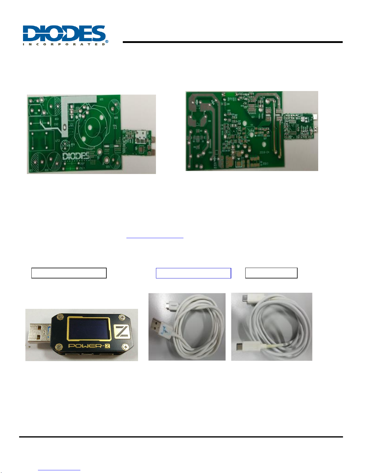
4.2 Quick Start Guide Before Connection
1) Before starting the 45W PD3.0 EVB test, the end user needs to prepare the following tool, software and manuals. For details,
please contact Chongdiantou Website (www.chongdiantou.com) for further information.
Test Kit: POWER-Z KM001 ( Chongdiantou Website’s PD3.0 Test Kit)
Figure 6: Items: Test Kit / Test Cables
2) Prepare a certified three-foot Type-C cable and a Standard-A to Micro-B Cable.
3) Connect the input AC L & N wires to AC power supply output “L and N “wires.
4) Ensure that the AC source is switched OFF or disconnected before the connection steps.
POWER-Z KM001 Test Kit
Standard-A to Micro-B Cable
Type-C Cable

45W USB PD 3.0 Adaptor EV1 Board User Guide
45W USB PD 3.0 AP3108L+APR346+CY2311 Page 9 of 28 7-1-2018
Release 1.0 www.diodes.com
Figure 7: The Sample Board Input & Output Location
5) A type-C cable for the connection between EVB’s and KM001’s Type-C receptacles.
6) Use 2 banana jack cables, one port of the cables are connected to E-load + & - terminals while the other port of the cables are
connected to EVB’s VBUS & GND pads.
7) A Standard-A to Micro-B cable to be connected to the KM001’s Micro-B receptacle & PC Standard-A receptacle respectively.
4.3 System Setup
4.3.1 Connection with E-Load
Figure 8: Diagram of Connections in the Sample Board

45W USB PD 3.0 Adaptor EV1 Board User Guide
45W USB PD 3.0 AP3108L+APR346+CY2311 Page 10 of 28 7-1-2018
Release 1.0 www.diodes.com
4.3.2 Canyon –Quick Charge 4/4+ Test Kit
Figure 9: The Test Kit Input & Output and E-load Connections
For details, please look for chongdiantou website for POWER-Z KM001 User Guide.
http://www.chongdiantou.com/wp/archives/13697.html
4.3.3 Input & Output Wires Connection
Figure 10: Wire Connection of 45W PD3.0 EVB to Test Kit and PC Computer
Micro-B Connector,
Connected to 5V source
Type-C Connector,
Connected to travel
charger
45W USB PD 3.0 Adaptor EV1 Board User Guide
45W USB PD 3.0 AP3108L+APR346+CY2311 Page 11 of 28 7-1-2018
Release 1.0 www.diodes.com
Chapter 5. Testing the Evaluation Board
5.1 Input & Output Characteristics
5.1.1 Input Standby Power
Note:
Standard Power test condition: The output terminal of power board don’t connected any load
5.1.2 Input Power Efficiency at Different AC Line Input Voltage
Vin
(Vac)
Freq
(HZ)
Vin
(V)
Iin(A)
PF
Pin
(W)
Vout
(V)
Iout
(A)
Pout
(W)
Pd
(W)
Eff
(%)
90
47
89.99
0.988
0.593
52.23
20.465
2.249
46.03
6.204
88.12
115
60
115.1
0.828
0.529
51.03
20.468
2.249
46.03
4.997
90.21
230
50
230.34
0.562
0.389
50.35
20.47
2.249
46.04
4.313
91.43
264
63
264.22
0.492
0.388
50.46
20.466
2.249
46.03
4.432
91.22
90
47
89.99
1.002
0.584
52.53
15.335
2.997
45.96
6.571
87.49
115
60
115.1
0.853
0.521
51.13
15.336
2.997
45.96
5.168
89.89
230
50
230.35
0.563
0.387
50.35
15.34
2.997
45.97
4.376
91.31
264
63
264.33
0.487
0.388
49.98
15.34
2.997
45.97
4.006
91.98
90
47
90.02
0.815
0.573
42.03
12.256
2.997
36.73
5.299
87.39
115
60
115.12
0.715
0.501
41.2
12.258
2.997
36.74
4.463
89.17
230
50
230.35
0.465
0.373
39.98
12.256
2.997
36.73
3.249
91.87
264
63
264.32
0.4
0.381
40.31
12.256
2.997
36.73
3.579
91.12
90
47
90.04
0.641
0.545
31.5
9.172
2.997
27.49
4.012
87.27
115
60
115.14
0.588
0.461
31.26
9.172
2.997
27.49
3.772
87.94
230
50
230.37
0.354
0.37
30.24
9.172
2.997
27.49
2.752
90.90
264
63
264.33
0.305
0.375
30.23
9.172
2.997
27.49
2.742
90.93
90
47
90.08
0.403
0.495
17.96
5.07
2.997
15.19
2.765
84.60
115
60
115.17
0.361
0.429
17.86
5.071
2.997
15.20
2.662
85.09
230
50
230.4
0.205
0.361
17.06
5.07
2.997
15.19
1.865
89.07
264
63
264.33
0.181
0.358
17.10
5.07
2.997
15.19
1.905
88.86
Output Voltage InputVoltage Standby Power (mW)
@ 5V 115Vac 60Hz 18mW
230Vac50Hz 24mW
45W USB PD 3.0 Adaptor EV1 Board User Guide
45W USB PD 3.0 AP3108L+APR346+CY2311 Page 12 of 28 7-1-2018
Release 1.0 www.diodes.com
5.1.3 Average Efficiency at Different Loading ( @ PCB end)
Vin
Vo
25%
Load
50%
Load
75%
Load
100%
Load
Average
Efficiency
Energy Star
Level VI
COC_Tier2
10% Load
Efficiency
115V/60Hz
5V-3A
88.77%
89.44%
89.08%
88.2%
88.87%
>81.39%
>81.84%
82.54%
9V -3A
90.22%
90.94%
90.68%
90.49%
90.50%
>86.62%
>87.30%
83.41%
12V3A
90.48%
90.96%
90.79%
89.11%
90.34%
>87.40%
>88.30%
86.58%
15V-3A
90.4%
90.96%
90.68%
89.87%
90.48%
>87.73%
>88.85%
86.41%
20V-2.25A
88.8%
89.93%
89.99%
89.93%
89.66%
>87.73%
>88.85%
82.67%
230V/50Hz
5V-3A
85.03%
87.29%
88.08%
87.89%
87.07%
>81.39%
>81.84%
80.33%
9V -3A
88.13%
90.38%
90.79%
90.72%
90.01%
>86.62%
>87.30%
80.04%
12V3A
89.16%
90.95%
91.25%
91.02%
90.59%
>87.40%
>88.30%
84.38%
15V-3A
89.47%
91.38%
91.36%
91.13%
90.83%
>87.73%
>88.85%
83.31%
20V-2.25A
87.98%
90.79%
91.12%
91.09%
90.25%
>87.73%
>88.85%
79.95%
5.2 Key Performance Waveforms
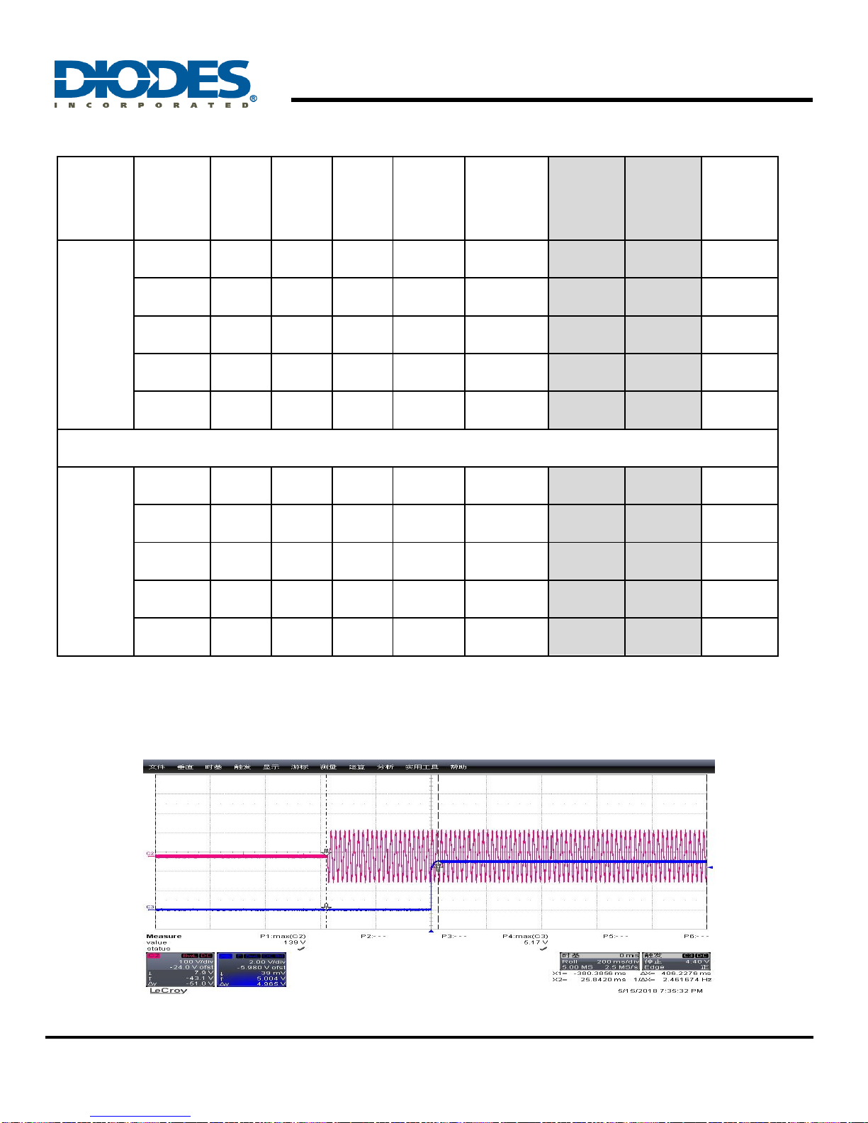
5.2.1 45W PD3.0 System Start-up Time & Hold-up Time
Figure 11: 45W PD 3.0 turn on time 0.406s 5V/3A at 90Vac
45W USB PD 3.0 Adaptor EV1 Board User Guide
45W USB PD 3.0 AP3108L+APR346+CY2311 Page 13 of 28 7-1-2018
Release 1.0 www.diodes.com
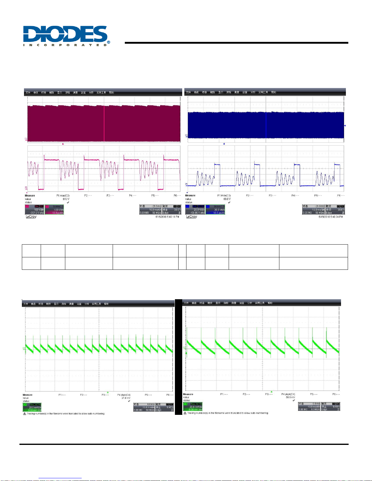
5.2.2 Q1 /Q2 Main Switching Voltage MOSFET Stress on at 20V/ 2.25A Loading @264Vac
Primary side MOSFET - Q1 Secondary side SR MOSFET- Q2
Figure 12: Q1 Vds Voltage stress Figure13: Q2 of Vds Voltage stress
5.2.3 System Output Ripple & Noise with @ PCB End
Figure 14: The Ripple at 90Vac/60Hz ΔV=27.8mV 5V/0A Figure 15: The Ripple at 264Vac/50Hz ΔV=58.8mv 5V/0A
Vout
Vds(V)
Vds_Max_Spec
Ratio of voltage stress
Vout
VR (v)
VRM_Max_Spec
Ration of voltage
stress
20V
613V
650V
94%
20V
88V
100V
88%

45W USB PD 3.0 Adaptor EV1 Board User Guide
45W USB PD 3.0 AP3108L+APR346+CY2311 Page 14 of 28 7-1-2018
Release 1.0 www.diodes.com
Figure 16: 90Vac/60Hz 5V/3A ΔV=96mV Figure 17: 264Vac/50Hz 5V/3A ΔV=122mv
Figure 18: 90Vac/60Hz 9V/0A ΔV=51.1mV Figure 19: 264Vac/50Hz 9V/0A ΔV=54mv
Figure 20: 90Vac/60Hz 9V/3A ΔV=98mV Figure 21: 264Vac / 60Hz 9V/3A ΔV=145mV

45W USB PD 3.0 Adaptor EV1 Board User Guide
45W USB PD 3.0 AP3108L+APR346+CY2311 Page 15 of 28 7-1-2018
Release 1.0 www.diodes.com
Figure 22: 90Vac/60Hz 12V/0A ΔV=33mV Figure 23: 264Vac / 60Hz 12V/0A ΔV=61mV
Figure 24: 90Vac/60Hz 12V/3A ΔV=111mV Figure 25: 264Vac / 60Hz 12V/3A ΔV=128mV
Figure 24: 90Vac/60Hz 15V/0A ΔV=59mV Figure 25: 264Vac / 60Hz 15V/0A ΔV=62mV

45W USB PD 3.0 Adaptor EV1 Board User Guide
45W USB PD 3.0 AP3108L+APR346+CY2311 Page 16 of 28 7-1-2018
Release 1.0 www.diodes.com
Figure 26: 90Vac/60Hz 15V/3A ΔV=164mV Figure 27: 264Vac / 60Hz 15V/3A ΔV=131mV
Figure 28: 90Vac/60Hz 20V/0A ΔV=34mV Figure 29: 264Vac / 60Hz 20V/0A ΔV=58mV
Figure 30: 90Vac/60Hz 20V/2.25A ΔV=162mV Figure 31: 264Vac / 60Hz 20V/2.25A ΔV=141mV

45W USB PD 3.0 Adaptor EV1 Board User Guide
45W USB PD 3.0 AP3108L+APR346+CY2311 Page 17 of 28 7-1-2018
Release 1.0 www.diodes.com
5.2.4 Dynamic load ----0A-3A 10mS 125mA/uS( PCB End)
Figure 32: 5V 0 ~ 3A Figure 33: 9V 0 ~ 3A
Figure 34: 5V 0 ~ 3A Figure 35: 9V 0 ~ 3A
Vin=264V Vo_Undershoot(V) Vo_Overshoot(V)
5V 4.729 5.521
9V 8.856 9.64
Vin=90V
Vo_Undershoot(V)
Vo_Overshoot(V)
5V
4.637
5.347
9V
8.629
9.358

45W USB PD 3.0 Adaptor EV1 Board User Guide
45W USB PD 3.0 AP3108L+APR346+CY2311 Page 18 of 28 7-1-2018
Release 1.0 www.diodes.com
Figure 36: 12V 0 ~ 3A Figure 37: 15V 0 ~ 3A
Figure 38: 12V 0 ~ 3A Figure 39: 15V 0 ~ 3A
Figure 40: 20V 0 ~ 3A @ 90Vac Figure 41: 20V 0 ~ 3A @264Vac
Vin=90V
Vo_
Undershoot(V)
Vo_ Overshoot(V)
12V
11.612
12.365
15V
14.55
15.425
Vin=264V
Vo_ Undershoot(V)
Vo_ Overshoot(V)
12V
11.587
12.431
15V
14.552
15.433

45W USB PD 3.0 Adaptor EV1 Board User Guide
45W USB PD 3.0 AP3108L+APR346+CY2311 Page 19 of 28 7-1-2018
Release 1.0 www.diodes.com
Vin=90V
Vo_
Undershoot(V)
Vo_ Overshoot(V)
20V
19.627
20.412
5.2.5 Output Voltage Transition Time
From Step up & Step down
Figure 42: 5V-9V-12V-15V-20V Transition Step Up Time Figure 43: 5V-9V-12-15V-20V Transition Steo down Time
Transition time from Low to high
Figure 44: 5V→9V Transition upl Time: 46ms Figure 45: 9V→12V Fall Time: 41ms
Vin=264V
Vo_
Undershoot(V)
Vo_ Overshoot(V)
20V
19.656
20.428

45W USB PD 3.0 Adaptor EV1 Board User Guide
45W USB PD 3.0 AP3108L+APR346+CY2311 Page 20 of 28 7-1-2018
Release 1.0 www.diodes.com
Figure 46: 12V→15V Fall Time: 41ms Figure 47: 15V→20V Fall Time: 65ms
Figure 48: 5V→20V Fall Time: 211ms
Table of contents
Other Diodes Motherboard manuals

Diodes
Diodes AP3041EV1 User manual

Diodes
Diodes AP63300-EVM User manual

Diodes
Diodes AP3981D2 User manual

Diodes
Diodes ZXLD1374QEV1 User manual

Diodes
Diodes AL8400QEV1 User manual

Diodes
Diodes AP63356Q-EVM User manual

Diodes
Diodes ZXLD1370 EV4 User manual

Diodes
Diodes AP3981B User manual

Diodes
Diodes PI6CG18801 Mounting instructions

Diodes
Diodes AL5802EV1 User manual


