Elby Designs ASM-2 Instructions for use

ASM-2 Construction Guide
ELBY Designs - Laurie Biddulph
9 Follan Close, Kariong, NSW 2250, Australia
elby-designs@bigpond.com http://www.elby-designs.com
1 of 19
ASM-2 Construction Notes
For PCB Rev 2.3
February 5, 2020
Please note that this document is still currently under revision and we apologise for any errors or omissions.
Readers should feel free to email any comments to me at the address given below.

ASM-2 Construction Guide
ELBY Designs - Laurie Biddulph
9 Follan Close, Kariong, NSW 2250, Australia
elby-designs@bigpond.com http://www.elby-designs.com
2 of 19
When assembling the board we recommend one of the following two strategies:-
1) Assembly of the full board by component type. In this method the board is built up in
layers starting with resistors and diodes, then ICs, capacitors, trimpots and transistors.
One disadvantage of this approach is
that the unit cannot be tested until the
complete board has been assembled. I
use a PCB Assembly Jig (see
photograph) which means that I can
insert components and solder them
without having too bend the legs over
to retain them. This is a big bonus if
you wish to experiment with the board
as it makes component removal a lot
easier.
2) Assembly by module. In this method each module is assembled in its entirety one at a
time. Once assembled, the module can be tested with, in many, cases minimal external
componentry being added. One disadvantage of this method is that you will need to
connect some external components to some of the modules for testing and this will
require some connecting and disconnecting to allow for easy assembly of the next
stage. This approach does not work with my PCB Assembly Jig and the previous
method as the variations in component heights affects the height of the components on
the board preventing the component retainer from working properly.
Option (2) may suit users with less confidence in their assembly skills as they can quickly
determine if a module works properly and as to how things are going.
Once you have figured out what components you want to stuff, mark up the drawings to
show this.
Occasionally some components may become obsolete or very difficult to get hold of. In
these instances, substitute components are provided. Wherever possible, these will be pin
compatible (as well as functionally compatible) allowing them to be inserted in to the PCB
without modifications. However, this is not always possible and some components may
need to have their legs bent to fit the PCB location. We are continually on the lookout for
alternative substitutes and will replace components in our kits as approved substitutes
become available.
We recommend you read our General Construction Notes for general assembly guidance
and other useful information.
ASM-2 Construction Guide
ELBY Designs - Laurie Biddulph
9 Follan Close, Kariong, NSW 2250, Australia
elby-designs@bigpond.com http://www.elby-designs.com
3 of 19
General notes on the assembly of the ASM-2 PCB:
All resistors on the PCB are on a 0.4” pitch whilst most diodes are on a 0.3” pitch and so
these components can be generally preformed before insertion in to the pcb. Capacitors in
the range 1nF to 1uF are normally on a 0.2” pitch whilst smaller capacitors are either 0.2”
pitch (generally ceramics) or 0.4” pitch (polystyrene). Tantalums and electrolytics are
generally on a 0.2” pitch.
It is recommended that Integrated Circuits (IC) socketed. If used, we strongly recommend
using machine-turned-pin sockets as these offer better long-term use.
Wiring to the boards is made easier by having all of the module connections at the edges
of the PCB. We recommend running your cables around the outside of the boards in a
loom leaving the centre of the board clear. This will be a boon when setting up and
adjusting the modules and will also simplify debugging should it be needed. This will result
in slightly longer cable runs but this should not adversely affect the quality of the system
through induced noise. Colour coding of cables is not a pre-requisite but once again using
colour-coded cables will simplify tracing faults. The table below gives two examples of
suggested colour schemes:-
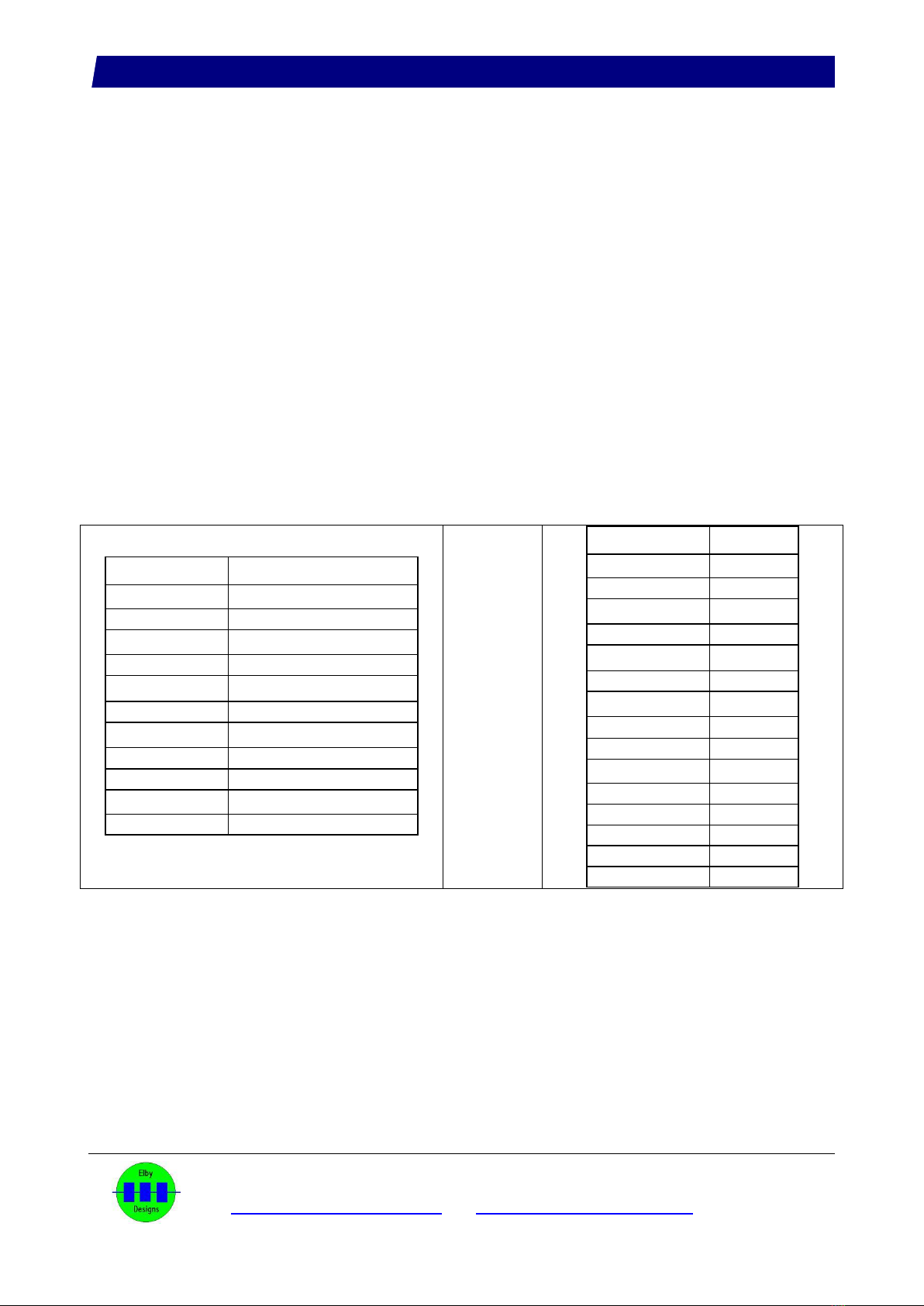
Cable Colour
Function
Red
+12V
Black
0V
Blue
-12V
Orange
Control Voltages - In
Pink
Control Voltages – Out
Grey
Signals – In*
White
Signals – Out*
OR
Cable Colour
Function
Red/White
+12V
Black/White
0V
Blue/Grey
-12V
Brown
Pin 1
Red
Pin 2
Orange
Pin 3
Yellow
Pin 4
Green
Pin 5
Blue
Pin 6
Violet
Pin 7
Grey
Pin 8
White
Pin 9
Pink
Pin 10
Black
Pin 11
* Audio signals are better wired using screened audio cable.
The first scheme on the left will have the advantage of allowing you to bulk buy a handful
of cable colours but will make fault finding a little harder.
The second scheme, on the right, will require smaller quantities of more cable colours but
will allow you to trace wires for a given module more easily. I would recommend this
second approach for beginners. In this scheme the colours are associated to the pin
number of the connector on the PCB

ASM-2 Construction Guide
ELBY Designs - Laurie Biddulph
9 Follan Close, Kariong, NSW 2250, Australia
elby-designs@bigpond.com http://www.elby-designs.com
4 of 19
For the choice of wire type and sizes we would suggest:-
7/0.2mm (24AWG – 7/32AWG) for control wires
16/0.2mm (22AWG – 7/30AWG) for power rails (NB: 7/0.2mm is also fine for this
purpose
Single-core screened audio cable for all signal wires
When selecting audio cable, choose the smallest outside diameter possible. I use
10/0.12mm with an OD of 1.6mm. Larger cable OD will result in a larger cable loom. When
connecting screened cable you should only connect one end of the screen to GND. In the
ASM1-Genie this GND connection was provided by running a length of tinned copper wire
around the outside of the pcb. This was achieved by placing eyelets on each corner of the
pcb (using the pcb fixing holes to support the eyelets) and then attaching the wire to the
free end of the eyelets. This approach means that the screen terminations are evenly
spread around the board making it easier to maintain the wiring. The free end of the
screen is cut flush with the end of the outer sleeve of the cable and either shrouded with a
piece of heatshrink or masked by teasing the outer sleeve over the exposed wire.
It is recommended that you treat all semiconductor parts as static-sensitive, especially the
CA3140s (be really careful with these – they are unbelievably easy to blow up).
Component Substitutions and Your Own Modifications:
If you know what you’re doing, go for it. If not, stick with the recommended parts.
TEMPCO’s:
The ASM kits include a TEMPCO resistor for each of the VCO’s. A TEMPCO can also be
used in the VCF but is not included in the kit as this is less critical. The ASM kits provide a
1% metal film resistor for the VCF. The PCB has positions for the TEMPCO on the pcb but
builders are referred to the photo which shows one method for improving the thermal
bonding between the TEMPCO and the MATCHED-NPN. In this approach the TEMPCO is
actually placed directly underneath the MATCED-NPN. Thermal contact is improved
through the application of some heatsink compound.
The current design of the VCO modules requires TEMPCOs with a Positive Temperature
Coefficient (PTC) of 3300ppm. Your VCO module kits will contain one of the following
configurations for this component:-
1. A 3300ppm resistor. In this case resistors R137 and R187 should be replaced with a
wire link
2. A 3500ppm resistor. In this case your kit will also include 2 off 62R 50ppm resistors
which should be fitted in positions R137 and R187
Thermal contact:
All of the critical exponential converter components are physically placed next to each
other so that they can be in physical contact. The transistors and the TEMPCO resistors (if
used) should, ideally, be thermally bonded together with heatsink compound, for best
thermal results. This is totally optional and only for those who are after perfect
performance.

ASM-2 Construction Guide
ELBY Designs - Laurie Biddulph
9 Follan Close, Kariong, NSW 2250, Australia
elby-designs@bigpond.com http://www.elby-designs.com
5 of 19
Bills of Materials (BOMs):
Components are given 3 or 4 digit identifiers such as C301, R221 and Q1201. The first of
these three digits (two in the case of 4-digit numbers) relates to the schematic sheet
number on which the component can be found whilst the last 2-digits are a sequence
number for that component category on the sheet.
When building your own order for components you should note the following points:-
1. All resistors are 1% 0.5W Metal Film (MRS25 Series). In most cases these can be
replaced by lower tolerance (up to 10%) resistors. Also in most cases you can also use
Carbon Film. The pcb footprint is for a 0.4” axial component.
2. Capacitors in the range 1nF and 1000nF are generally Polyester (BF or MKS2 Series).
Substitutes should be of a low-noise, high-stability type. The pcb footprint is for 0.2”
pitch radial components.
3. Capacitors below 1nF are generally 2.5% 160VDC Polystyrene (FCS Series) but
Silvered Mica will also work fine. In some cases it is possible too use a high-stability
NPO Multilayer Ceramic capacitor. The pcb footprint is for 0.2” radial components.
4. Decoupling capacitors are listed as 100nF X7R Multilayer Ceramics. Values in the
range of 47nF to 150nF can be freely used in these positions and any good quality
capacitor that will fit the 0.2” radial footprint can be used.
5. Capacitors of 1uF and above are polarised and should either be MDT or TAP Series
Tantalum or low-impedance Aluminium Electrolytics. Tantalums are, typically for 0.2”
pitch devices
Some schematics include panel-mounted components. Where shown, these components
are required for the proper operation of the circuit. These components are NOT included in
ASM2 Component Kit.
A hard-copy of the component overlay can be printed using this ASM-2 PCB Overlay PDF
file. It is sized for A3.
3D Model

ASM-2 Construction Guide
ELBY Designs - Laurie Biddulph
9 Follan Close, Kariong, NSW 2250, Australia
elby-designs@bigpond.com http://www.elby-designs.com
6 of 19
VCO - Voltage Controlled Oscillator
TEMPCO
For optimum performance the VCO uses a
temperature compensation circuit that utilises a
TEMPCO resistor. For best results the
TEMPCO should be thermally bonded to the
matched transistor pair Q101/Q151. The picture
to the right shows how the TEMPCO should be
mounted. If desired, thermal bonding can be
improved further by the addition of some
heatsink compound.
Assembly Modifications
R106 on the PCB should be replaced with a wire link. R106 and an additional 100K 0.1%
resistor (XR106) will then be wired in series with S110 [KCV] and S101 [TRANSPOSE] on
the panel.
R156 on the PCB should be replaced with a wire link. R156 and an additional 100K 0.1%
resistor (XR149) will then be wired in series with S160 [KCV] and S151 [TRANSPOSE] on
the panel.
R110 on the PCB should be replaced with a wire link. R110 and an additional 100K
resistor (XR149) will then be wired in series with pots P117 [PWM1] and P119 [PWM2] on
the panel.
A significant improvement in the quality of the Sawtooth output (and hence the Triangle
and Sine) can be achieved by performing this modification to U101 and U151.
1. Cut the leg at the shoulder, of pin 4 of the 8-pin wire-
wrap socket for U101/U151 - see image at left
2. Use a small piece of wire offcut and solder a bridge
between pin 3 and the shortened pin 4 - see image at
right
3. Install the socket on to the pcb ensuring that there is a
small gap between pin 4 of the socket and the pcb

ASM-2 Construction Guide
ELBY Designs - Laurie Biddulph
9 Follan Close, Kariong, NSW 2250, Australia
elby-designs@bigpond.com http://www.elby-designs.com
7 of 19
Power up, Testing and Calibration Procedures
Setting up of the VOLT/OCTAVE requires an accurate and stable voltage source. If using
a MIDI-CV device then you should use that to ensure that the VCOs are tuned to your
MIDI device.
1. Disconnect all control inputs (2 x PWM, 2 x LIN FM and 6 x LOG FM) -alternately,
measure each of the inputs and adjust its associated control for a reading of 0.0V
2. Monitor the SAWTOOTH output with a frequency counter or scope
3. Open LK100 (LK150) to disable the `INIT FREQ’ trimpot
4. Adjust P101 (P151) for a frequency of 880Hz
5. Apply 3.0V to one of the LOG FM inputs
6. Adjust P107 (P157) to give a frequency of 7.04kHz
Having set the VOLT/OCTAVE characteristics of the VCO, we can now finalise the setting
up of the VCO.
7. Insert LK100 (LK150)
8. Apply 5.0V (MIDI Note = 60) to one of the LOG FM inputs
9. Adjust `INIT FREQ’ (P100/P150) to give a reading of 261.626Hz.
10.Remove the 5.0V on the LOG FM input
11.Confirm that the output frequency is 8.176Hz
It is worth repeating these steps to ensure that the settings are stable.
This completes the setting up of the VCO. Reconnect all control inputs.
The VCO can now be connected to a 1V/Octave MIDI-CV module and will play the correct
frequency for a given MIDI Note Number as per the MIDI Note Table included with this
documentation (assuming all other control voltages are at 0.0V).
Square Waveform Adjustment
1. The Square output does not need adjustment. Monitor the Square output on J102
(J152) and check that the waveform is centered around 0V.
Triangle Waveform Adjustment
1. Monitor the Triangle output on J102 (J152) and using P103 (P153) adjust the output
until it is centered around 0V.
1. Using P105 (P155) adjust the output until the positive and negative slopes are identical,
2. Using P104 (P154) adjust the output to minimise the glitch at the bottom of the
waveform,
3. Finally, using P106 (P156) adjust the output until is centered around 0V.
Sine Waveform Adjustment
1. Monitor the Sine output on J102 (J152) and using P102 (P152) adjust the output for a
peak-peak output of 10V.

ASM-2 Construction Guide
ELBY Designs - Laurie Biddulph
9 Follan Close, Kariong, NSW 2250, Australia
elby-designs@bigpond.com http://www.elby-designs.com
8 of 19
VCF - Voltage Controlled Filter (VCF 1)
Power up, Testing and Calibration Procedures:
There are three trimmers on the PCB:-
V/OCT (P201): This adjusts the scaling of the exponential inputs. Adjust this so that there
is an octave jump in cut-off frequency when the 1V/OCT input is raised by one volt.
Plug a 1V/octave source into one of the CV inputs. This may be your keyboard’s pitch CV
output, or from the CV output of a midi-CV converter. Set the Resonance pot P204 fully
clockwise to get the filter oscillating. Now listen to the output coming from the low pass
output. You may find it best to use the Frequency pot on the front panel to set the filter
oscillating at quite a high frequency tone. Somewhere around 1KHz will do. Now play a
note on your keyboard and then the same note an octave above. Repeat this again and
again and adjust the V/OCT trimmer to get the filter’s oscillations to jump an octave too.
Don’t worry about the actual pitch the VCF is producing. Just concentrate on getting
roughly one octave difference between the low note and the high note. It is a fiddly
adjustment and it takes a while to get it right. But remember that this is a filter and not a
VCO, so you don’t have to be too accurate.
OFFSET: The two OFFSET trimmers (P202 and P203) control the amount of DC on the
output. Use a scope or a voltmeter to measure the voltage at pin 1 of U204. Rotate the
Frequency pot until the voltage is approximately zero volts. Without any audio input,
measure the voltage at the BP output. Set OFFSET 2 so that the voltage at the BP output
is as close to zero as you can get it. You should be able to get it down to +/-5mV or less.
Now measure the voltage at the LP output. Set OFFSET 1 so that this voltage is as close
to zero as you can get it. Again aim for +/-5mV or less.

ASM-2 Construction Guide
ELBY Designs - Laurie Biddulph
9 Follan Close, Kariong, NSW 2250, Australia
elby-designs@bigpond.com http://www.elby-designs.com
9 of 19
VCF - Voltage Controlled Filter (VCF 2)
Power up, Testing and Calibration Procedures:
TEMPERATURE OVEN ADJUSTMENT
NOTE
This adjustment should be made at 22˚C (72˚F) if possible. If not, use the appropriate
correction factor shown in Table 1
Before applying power to the board, fit JP801. If power has already been connected,
fit JP801 and allow a five minute warm-up period before making the next
measurement
Measure and note the voltage at TP15
Remove JP801 and adjust P807 until the reading is 60mV below the original
reading
Wait 30 seconds and readjust if necessary.
˚C
˚F
mV DROP
16
62
70
19
67
65
22
72
60
25
77
55
28
82
50
Table 1: Correction Factor
Here's a procedure without a scope. The basic idea is that you use the
VCF as an oscillator, with Emphasis all the way up. A well-tuned VCO acts as
a reference, so the VCF should follow the VCO when CV changes.
Apply a control voltage (CV) to the VCF and a VCO
Turn the Emphasis (P805) pot all the way up so that the filter starts to oscillate:
you'll hear a sine wave without any input signal to the filter
Tune both VCO and VCF to the same frequency for a key on the keyboard,
say 1000Hz, so you have zero beatings.
Press a key two octaves up. Adjust P802 so that you get zero beatings
again, thus the filter gives the same frequency as the VCO.
Press a lower key and tune the filter manually to the VCO frequency
again with P801 (Frequency).
Press the higher key again and adjust P802 so you get zero
beatings.
Repeat this process a few times.

ASM-2 Construction Guide
ELBY Designs - Laurie Biddulph
9 Follan Close, Kariong, NSW 2250, Australia
elby-designs@bigpond.com http://www.elby-designs.com
10 of 19
Emphasis Trim (P804) and VCF Balance (P803) don't have much effect. You only need to
adjust them when you're very picky otherwise turn P804 to minimum
resistance and P803 to the mid position.
P807 should be set to its center position.

ASM-2 Construction Guide
ELBY Designs - Laurie Biddulph
9 Follan Close, Kariong, NSW 2250, Australia
elby-designs@bigpond.com http://www.elby-designs.com
11 of 19
ADSR Envelope Generator
Power up, Testing and Calibration Procedures:
ADSR 1
MAXIMUM ENVELOPE
1. Monitor TP9 and adjust P400 for 5V0
ATTACK PEAK
1. Set [ATTACK], [DECAY] and [RELEASE] to minimum and [SUSTAIN] to maximum.
2. Set P406 fully clockwise
3. Apply a low-frequency square wave (around 1-5Hz will be fine) to the GATE input
4. Monitor [ADSR 1 OUT] which should exhibit a square wave in time with the frequency
of the GATE signal
5. Adjust P406 so that the rising edge of the envelope peaks at 5V0 and that there is no
overshoot or undershoot.
This completes the setting up for the ADSR 1 module.
ADSR 2
MAXIMUM ENVELOPE
1. Monitor TP11 and adjust P450 for 5V0
ATTACK PEAK
1. Set [ATTACK], [DECAY] and [RELEASE] to minimum and [SUSTAIN] to maximum.
2. Set P456 fully clockwise
3. Apply a low-frequency square wave (around 1-5Hz will be fine) to the GATE input
4. Monitor [ADSR 2 OUT] which should exhibit a square wave in time with the frequency
of the GATE signal
5. Adjust P456 so that the rising edge of the envelope peaks at 5V0 and that there is no
overshoot or undershoot.
This completes the setting up for the ADSR 2 module.
ATTACK PEAK Adjustment

ASM-2 Construction Guide
ELBY Designs - Laurie Biddulph
9 Follan Close, Kariong, NSW 2250, Australia
elby-designs@bigpond.com http://www.elby-designs.com
12 of 19
VCA (1)(2) - Voltage Controlled Amplifier
Apply xV
Monitor TP13 and adjust P301 for minimum output
Monitor TP14 and adjust P351 for minimum output

ASM-2 Construction Guide
ELBY Designs - Laurie Biddulph
9 Follan Close, Kariong, NSW 2250, Australia
elby-designs@bigpond.com http://www.elby-designs.com
13 of 19
Noise Module
Power up, Testing and Calibration Procedures:
1. Monitor the [WHITE] noise output
2. Adjust P601 for a nominal output of 5Vpk-pk
A socket should, ideally, be fitted for T601 so that a range of transistors can be tried to
obtain optimum noise levels. The white noise output should be between 2.0 and 2.8V
peak-to-peak. Different transistors should be tested along with varying the value of P601.

ASM-2 Construction Guide
ELBY Designs - Laurie Biddulph
9 Follan Close, Kariong, NSW 2250, Australia
elby-designs@bigpond.com http://www.elby-designs.com
14 of 19
VCLFO - Low Frequency Oscillator
Power up, Testing and Calibration Procedures:
LFO 1 Offset Adjustment
1. Fit a jumper between JP501_2 and JP501_3.
2. Monitor TP7 with a multimeter. It will probably exhibit a tendency to drift positive or
negative, and the voltage will settle at +Ve or –Ve.
3. Reset the output voltage to zero by holding a 1K resistor between TP7 and JP502.
4. Adjust P504 until the voltage remains stable at zero volts for a period of several
seconds (without the discharge resistor in circuit).
5. Repeat steps (3) and (4), progressively switching the multimeter to more sensitive
ranges, until the drift is only a few hundred millivolts in several seconds.
6. Return jumper to JP501_1 and JP501_2
LFO 1 BEAT LED Adjustment
P505 should be adjusted so that the brightness of the LED follows the amplitude of the
triangle output, i.e. the LED brightness should be at minimum brightness when the triangle
is at its most negative, and at maximum brightness when the triangle is at its most positive.
LFO 2 Offset Adjustment
7. Fit a jumper between JP551_2 and JP551_3.
8. Monitor TP8 with a multimeter. It will probably exhibit a tendency to drift positive or
negative, and the voltage will settle at +Ve or –Ve.
9. Reset the output voltage to zero by holding a 1K resistor between TP8 and JP552.
10.Adjust P554 until the voltage remains stable at zero volts for a period of several
seconds (without the discharge resistor in circuit).
11.Repeat steps (3) and (4), progressively switching the multimeter to more sensitive
ranges, until the drift is only a few hundred millivolts in several seconds.
12.Return jumper to JP551_1 and JP551_2
LFO 2 BEAT LED Adjustment
P555 should be adjusted so that the brightness of the LED follows the amplitude of the
triangle output, i.e. the LED brightness should be at minimum brightness when the triangle
is at its most negative, and at maximum brightness when the triangle is at its most positive.


ASM-2 Construction Guide
ELBY Designs - Laurie Biddulph
9 Follan Close, Kariong, NSW 2250, Australia
elby-designs@bigpond.com http://www.elby-designs.com
16 of 19
Ring Modulator
Power up, Testing and Calibration Procedures
Setting up the circuit is quite straight-forward but needs to be done carefully. You will need
a 10V p-p sine or triangle wave of about 1kHz and either an oscilloscope, sensitive AC
voltmeter or an audio amplifier.
1. Monitor 'TP4 RING' of the Ring Modulator.
2. Apply the test signal to the [CARRIER] input (J1601 pin 1).
3. Adjust P1601 until the output signal is at minimum.
4. Apply the test signal to the [SIGNAL] input (J1601 pin 2).
5. Adjust P1602 until the output signal is at minimum.
6. Repeat steps (2) to (5) until no further improvement can be made.
The level of feed-through obtained will vary between IC’s. Typically, with a 10V p-p signal
the feed-through for the [CARRIER] input may be trimmed to between 10mV (-60dB) and
20mV (-54dB). For the [SIGNAL] input this will, typically, be between 40mV (-48dB) and
80mV (-42dB).

ASM-2 Construction Guide
ELBY Designs - Laurie Biddulph
9 Follan Close, Kariong, NSW 2250, Australia
elby-designs@bigpond.com http://www.elby-designs.com
17 of 19
Sample & Hold
The Sample & Hold circuit has a small pcb footprint error. C901 should be replaced with a
resistor which can be simply stood on end to fit the board.
Power up, Testing and Calibration Procedures

ASM-2 Construction Guide
ELBY Designs - Laurie Biddulph
9 Follan Close, Kariong, NSW 2250, Australia
elby-designs@bigpond.com http://www.elby-designs.com
18 of 19
PSU
There is a pcb error with U3 and U4. Please refer to the ASM Overlay PDF for the correct
installation orientation.
The PCB silkscreen also indicates that the internal reference supplies are 7V, this has
been updated to 9V.
These internal reference supplies, available at J3, are to be used only for the VCOs.
J2 is available for other panel components that require access to the main power rails (+/-
12V)
Power up, Testing and Calibration Procedures
1. Monitor TP2 and adjust P1 (+7V) for +9.0V
2. Monitor TP3 and adjust P2 (-7V) for -9.0V

Table of contents
Other Elby Designs Synthesizer manuals

Elby Designs
Elby Designs CGS738 Instructions for use

Elby Designs
Elby Designs EURO STAGE ES30 Instructions for use

Elby Designs
Elby Designs EURO SERGE ASM301 Instructions for use
 User manual")
Elby Designs
Elby Designs MonoWave(X) User manual

Elby Designs
Elby Designs Pixie Attache EDP WASP User manual

Elby Designs
Elby Designs IF101 2Q/4Q Instructions for use

Elby Designs
Elby Designs EURO-SERGE User manual
 User manual")
Elby Designs
Elby Designs MonoWave(X) User manual

Elby Designs
Elby Designs ASM321 Instructions for use


