Embedded Artists EA-QSB-010 User manual
LPC4357 Developer’s Kit - User’s Guide
Copyright 2013 © Embedded Artists AB
EA2-USG-1208 Rev A
LPC4357 Developer’s Kit
User’s Guide
Get Up-and-Running Quickly and
Start Developing Your Application On Day 1!

LPC4357 Developer’s Kit - User’s Guide
Page 2
Copyright 2013 © Embedded Artists AB
Embedded Artists AB
Davidshallsgatan 16
211 45 Malmö
Sweden
info@EmbeddedArtists.com
http://www.EmbeddedArtists.com
Copyright 2013 © Embedded Artists AB. All rights reserved.
No part of this publication may be reproduced, transmitted, transcribed, stored in a retrieval system, or
translated into any language or computer language, in any form or by any means, electronic,
mechanical, magnetic, optical, chemical, manual or otherwise, without the prior written permission of
Embedded Artists AB.
Disclaimer
Embedded Artists AB makes no representation or warranties with respect to the contents hereof and
specifically disclaim any implied warranties or merchantability or fitness for any particular purpose.
Information in this publication is subject to change without notice and does not represent a
commitment on the part of Embedded Artists AB.
Feedback
We appreciate any feedback you may have for improvements on this document. Please send your
comments to support@EmbeddedArtists.com.
Trademarks
All brand and product names mentioned herein are trademarks, services marks, registered
trademarks, or registered service marks of their respective owners and should be treated as such.

LPC4357 Developer’s Kit - User’s Guide
Page 3
Copyright 2013 © Embedded Artists AB
Table of Contents
1Document Revision History 5
2Introduction 6
2.1 Features 6
2.2 ESD Precaution 7
2.2.1 ESD sensitivity on JTAG interface 8
2.3 General Handling Care 8
2.4 Code Read Protection 8
2.5 CE Assessment 8
2.6 Other Products from Embedded Artists 9
2.6.1 Design and Production Services 9
2.6.2 OEM / Education / QuickStart Boards and Kits 9
3LPC4357 OEM Board Design 10
3.1 Memory Layout 10
3.1.1 NAND Flash 10
3.2 SPIFI 11
3.3 Bootloader Mode Setting 11
3.4 Trace Connector 12
3.5 I2S and SGPIO Connectors 12
3.6 uSD Memory Card Interface 12
3.7 Board Options 13
3.8 1 kBit I2C E2PROM with EUI-48™ Number 13
4OEM Base Board Design 14
4.1 Modifications to OEM Base Board 14
4.2 SP2: OEM Board Connector 15
4.3 SP2: Current Measurements 15
4.4 SP3: Expansion Connectors 15
4.5 SP4: External Memory Bus 16
4.6 SP5: Debug Interfaces 17
4.7 SP6: Ethernet Interface 19
4.8 SP6: SD/MMC Memory Card Interface 20
4.9 SP6: VBAT/ALARM Handling 21
4.10 SP7: I2C Peripherals 22
4.11 SP8: Analog Input 23
4.12 SP8: Digital IO 24
4.13 SP8: Serial Expansion Connector 24
4.14 SP8: NXP/Jennic RF Module Interface 26
4.15 SP9: UART Multiplexing 27
4.16 SP9: RS232 Interface 28

LPC4357 Developer’s Kit - User’s Guide
Page 4
Copyright 2013 © Embedded Artists AB
4.17 SP9: RS422/485 Interface 29
4.18 SP10: CAN 30
4.19 SP10: IrDA 31
4.20 SP11: USB Channel 1 32
4.20.1 USB Channel 1 as USB Host 33
4.20.2 USB Channel 1 as USB Device 33
4.20.3 USB Channel 1 as USB OTG 33
4.21 SP12: USB Channel 2 34
4.21.1 USB Channel 2 (USB0 on LPC4357) as USB Host 35
4.21.2 USB Channel 2 (USB0 on LPC4357) as USB Device 35
4.21.3 USB Channel 2 (USB0 on LPC4357) as USB OTG 35
4.22 SP13: UART-to-USB Bridge 36
4.23 SP13: Power Supply 37
4.24 SP14: LCD Expansion Interface 37
4.25 SP15: I2S Audio Codec 38
4.26 Default Jumpers Positions 40
4.27 Usage of CPU Pins 41
5Getting Started 47
5.1 Powering 47
5.2 Demo Application 47
5.3 Installing USB Driver 49
5.4 Program Download 49
5.4.1 ISP over USB Program Download 50
5.5 Handling SO-DIMM Boards 54
5.6 Things to Note 54
5.6.1 Humming in Speaker 54
5.6.2 Current Consumption and Limits of USB Ports 55
5.6.3 LCD flickering 55
5.6.4 Initialization of External Memory Bus 56
5.6.5 USB OTG Transceiver 56
6LCD Expansion Connector 57
7Troubleshooting 60
7.1 No SWD/JTAG Connection 60
7.2 Powering 60
7.3 Contact with OEM Board MCU 61
7.4 Using Test Program to Verify Correct Operation 61
8Further Information 62
LPC4357 Developer’s Kit - User’s Guide
Page 5
Copyright 2013 © Embedded Artists AB
1 Document Revision History
Revision
Date
Description
PA1
2012-10-29
First version.
PA2
2012-12-08
Added information about ESD sensitive JTAG interface.
PA3
2013-01-21
Minor clarifications.
PA4
2013-04-08
Clarified that JP4 must be shorted (jumper installed) in order for the
LPC4357 SWD/JTAG interface to function.

LPC4357 Developer’s Kit - User’s Guide
Page 6
Copyright 2013 © Embedded Artists AB
2 Introduction
Thank you for buying Embedded Artists’ LPC4357 Developer’s Kit based on NXP’s ARM dual-core
Cortex-M4/M0 LPC4357 microcontroller.
This document is a User’s Guide that describes the LPC4357 OEM Board and the OEM Base Board
hardware design, which together form the LPC4357 Developer’s Kit.
2.1 Features
Embedded Artists’LPC4357 OEM Board lets you get up-and-running quickly. The small form factor
OEM board offers many unique features that ease your learning curve and program development. The
board has been designed for OEM applications with volume discount available.
NXP's ARM dual-core Cortex-M4/M0 LPC4357 microcontroller in BGA package, with 1 MByte
program FLASH and 136 KByte SRAM
16 MBit QSPI flash on SPIFI interface
External FLASH memories: 128 MB NAND FLASH
External data memory: 32 MB SDRAM (32-bit databus width)
12.0000 MHz crystal for maximum execution speed and standard serial bit rates, including
CAN and USB requirements
32.768kHz RTC crystal
100/10M Ethernet PHY/interface based on SMSC LAN8720
Buffered 32-bit data bus for external expansion
1 Kbit E2PROM with EUI-48™ number (for Ethernet MAC address)
200 pos expansion connector (SODIMM-200 format, 0.6mm pitch)
Most LPC4357 pins available (see LPC4357 OEM Board datasheet for details)
+3.3V only powering
Onboard reset generation
Compact SODIMM format: 68 x 50 mm
Eight layer PCB design for best EMC performance, with controlled impedance and length
matched routing for critical signals
There is an accompanying OEM Base Board that can be used for initial prototyping work. The features
of the board are:
Interfaces and Connectors
200 pos, 0.6mm pitch SODIMM connector for OEM Board
LCD expansion connector with control signals for touch screen interface
Expansion connector with all OEM Board signals
Ethernet connector (RJ45)
CAN interface & connector (provision for second CAN interface, but not mounted)
USB1: OTG or Host interface & connector

LPC4357 Developer’s Kit - User’s Guide
Page 7
Copyright 2013 © Embedded Artists AB
USB2: Device or Host interface & connector
Provision for NXP JN5148 RF module (former Jennic) interface (RF module not included)
Full modem RS232 (cannot be fully used on 32-bit databus OEM boards)
RS422/485 interface & connector
I2S audio codec (mic in, line in, line out, headphone out)
SWD/JTAG connector
Trace connector
Power
Power supply, either via USB or external +5V DC
Coin cell powering supported (CR1025 battery not incl.) for RTC and LED on ALARM sig.
Other
OEM Board current measuring
Parallel NOR flash on external memory bus
16-bit register and LEDs on external memory bus
5-key joystick
3-axis accelerometer (I2C connected)
LM75 temperature sensor (I2C connected)
5 push-button keys (four via I2C and one on P2.10)
9 LEDs (8 via I2C and one on P2.10)
Analog input
USB-to-serial bridge on UART #0 (FT232R) and ISP functionality
Reset push-button and LED
Speaker output on analog output from OEM Board, or from I2S audio codec
Compact size: 160x150 mm
2.2 ESD Precaution
Please note that the LPC4357 OEM Board and OEM Base Board come without
any case/box and all components are exposed for finger touches –and therefore
extra attention must be paid to ESD (electrostatic discharge) precaution.
Make it a habit always to first touch the metal surface of one of the USB or
Ethernet connectors for a few seconds with both hands before touching
any other parts of the boards. That way, you will have the same potential as
the board and therefore minimize the risk for ESD.
Never touch directly on the LPC4357 OEM Board and in general as little as possible on the OEM Base
Board. The push-buttons on the OEM Base Board have grounded shields to minimize the effect of
ESD.
Note that Embedded Artists does not replace boards that have been damaged by ESD.

LPC4357 Developer’s Kit - User’s Guide
Page 8
Copyright 2013 © Embedded Artists AB
2.2.1 ESD sensitivity on JTAG interface
Note that the LPC4357 MCU is sensitive to ESD on the JTAG port. Observe extra care around this.
Make sure the ground of the JTAG interface is connected to the OEM Base Board ground
before even connecting the JTAG interface. Never have the OEM Board unpowered while the
JTAG pod is powered.
2.3 General Handling Care
Handle the LPC4357 OEM Board and OEM Base Board with care. The boards are not mounted in a
protective case/box and are not designed for rough physical handling. Connectors can wear out after
excessive use. The OEM Base Board is designed for prototyping use, and not for integration into an
end-product.
For boards with LCD, do not exercise excessive pressure on the LCD glass area. That will damage the
display. Also, do not apply pressure on the flex cables connecting the LCD/touch screen. These are
relatively sensitive and can be damaged if too much pressure is applied to them.
Note that Embedded Artists does not replace boards where the LCD has been improperly
handled.
2.4 Code Read Protection
The LPC4357 has a Code Read Protection function (specifically CRP3, see datasheet for details) that,
if enabled, will make the LPC4357 impossible to reprogram (unless the user program has implemented
such functionality).
Note that Embedded Artists does not replace LPC4357 OEM boards where the LPC4357 has
CRP3 enabled. It’s the user’s responsibility to not invoke this mode by accident.
2.5 CE Assessment
The LPC4357 Developers Kit (consisting of the LPC4357 OEM Board and OEM Base Board) is CE
marked. See separate CE Declaration of Conformity document.
The LPC4357 Developers Kit is a class A product. In a domestic environment this product may cause
radio interference in which case the user may be required to take adequate measures.
EMC emission test has been performed on the LPC4357 Developers Kit. Standard interfaces like
Ethernet, USB, serial have been in use. General expansion connectors where internal signals are
made available (for example processor pins) have been left unconnected. Connecting other devices to
the product via the general expansion connectors may alter EMC emission. It is the user’s
responsibility to make sure EMC emission limits are not exceeded when connecting other devices to
the general expansion connectors of the LPC4357 Developers Kit.
Due to the nature of the LPC4357 Developers Kit –an evaluation board not for integration into an end-
product –fast transient immunity tests and conducted radio-frequency immunity tests have not been
executed. Externally connected cables are assumed to be less than 3 meters. The general expansion
connectors where internal signals are made available do not have any other ESD protection than from
the chip themselves. Observe ESD precaution.
Note that the LPC4357 OEM board is classified as a component and is hence not CE marked
separately. It can perform different functions in different integrations and it does not have a direct
function. It is therefore not in the scope of the CE Directive. An end product, where an OEM Board is
integration into, is however very likely to need CE marking.

LPC4357 Developer’s Kit - User’s Guide
Page 9
Copyright 2013 © Embedded Artists AB
2.6 Other Products from Embedded Artists
Embedded Artists have a broad range of LPC1000/2000/3000/4000 based boards that are very low
cost and developed for prototyping / development as well as for OEM applications. Modifications for
OEM applications can be done easily, even for modest production volumes. Contact Embedded Artists
for further information about design and production services.
2.6.1 Design and Production Services
Embedded Artists provide design services for custom designs, either completely new or modification to
existing boards. Specific peripherals and I/O can be added easily to different designs, for example,
communication interfaces, specific analog or digital I/O, and power supplies. Embedded Artists has a
broad, and long, experience in designing industrial electronics in general and with NXP’s
LPC1000/2000/3000/4000 microcontroller families in specific. Our competence also includes wireless
and wired communication for embedded systems. For example IEEE802.11b/g (WLAN), Bluetooth™,
ZigBee™, ISM RF, Ethernet, CAN, RS485, and Fieldbuses.
2.6.2 OEM / Education / QuickStart Boards and Kits
Visit Embedded Artists’ home page, www.EmbeddedArtists.com, for information about other OEM /
Education / QuickStart boards / kits or contact your local distributor.

LPC4357 Developer’s Kit - User’s Guide
Page 10
Copyright 2013 © Embedded Artists AB
3 LPC4357 OEM Board Design
Please read the LPC4357 OEM Board datasheet and associated schematic for information about the
board. Some additional information about the LPC4357 OEM Board is presented below.
3.1 Memory Layout
The external memory controller on the LPC4357 defines eight memory regions. See table below for
details about usage.
Name
Control
signal
Address range
Memories on LPC4357
OEM Board
External memory bus
comment
Static memory #0
CS0
0x1C00 0000 –
0x1CFF FFFF
Available for external
use.
OEM Base Board can
connect a parallel NOR
flash to this chip select.
Static memory #1
CS1
0x1D00 0000 –
0x1DFF FFFF
NAND FLASH (1 GBit =
128 MByte in size)
Not available for
external use.
It is however possible
to disable NAND flash
chip by removing R25
on LPC4357 OEM
Board.
Static memory #2
CS2
0x1E00 0000 –
0x1EFF FFFF
Available for external
use.
OEM Base Board can
connect a 16-bit parallel
register to this chip
select.
Static memory #3
CS3
0x1F00 0000 –
0x1FFF FFFF
Available for external
use.
Dynamic memory #0
DYCS0
0x2800 0000 –
0x2FFF FFFF
SDRAM (256 MBit = 32
MByte in size)
Cannot be accessed on
external memory bus.
Dynamic memory #1
DYCS1
0x3000 0000 –
0x3FFFF FFFF
Cannot be accessed on
external memory bus.
As seen in the table above, it is only the static memory regions that are available on the external
memory bus from the LPC4357 OEM Board. The data bus buffers on the LPC4357 OEM Board are
controlled automatically and only enabled when a static memory region is accessed. The address and
control bus buffers are always enabled.
Note that the BLS0, BLS1, BLS2 and BLS3 pins must be initialize for these functionalities. Else the
buffer control will not work correctly.
3.1.1 NAND Flash
Note that the NAND flash is connected after the memory bus buffers, i.e., on the same side as the
LPC4357 OEM Board expansion signals. This is to allow flexibility in NAND flash usage and reduce
loading on memory bus that is directly connected to the SDRAM.

LPC4357 Developer’s Kit - User’s Guide
Page 11
Copyright 2013 © Embedded Artists AB
The NAND FLASH has an optional busy output that can be used for controlling the erase/program
operations with better precision. The signal is available on the expansion connector. If needed, the
signal can be routed to a suitable (i.e., free) input pin. The OEM Base Board can connect the signal to
GPIO72 by inserting a jumper between pin 3-4 on JP2. The busy status of the chip is also available
under software control.
3.2 SPIFI
There is a 16 MBit QSPI flash connected to the SPIFI interface of the LPC4357. This memory region is
available in the following address region: 0x1400 0000 –0x1800 0000.
3.3 Bootloader Mode Setting
There are several boot modes for the LPC4357 microcontroller. For details, read the LPC4357 User’s
manual. The LPC4357 OEM board has four sliders switches, JP1, where the boot mode can bet set.
Note that there are situations where the slider switch settings do not affect boot more. Read the
LPC4357 User’s manual for details about this, but in general the slider settings will be used to
determine the boot mode when P2_7 is pulled low during reset. This is accomplished by pulling pin
ISP_EN low, which in turn is accomplished by pressing SW6 on the OEM base board during reset. If
signal P2_7 is high during reset the LPC4357 boos from internal FLASH by default.
Schematic page 2 of the LPC4357 OEM board contains a list of the boot modes and associated slider
settings for JP1.
LED3 on the LPC4357 OEM board is connected to signal P1_1-A6-BS0, and is used by the
microcontroller to signal possible errors during booting. LED3 will flash with a 1 Hz rate for 60 seconds
if the boot process fails. After 60 seconds, the device is reset.
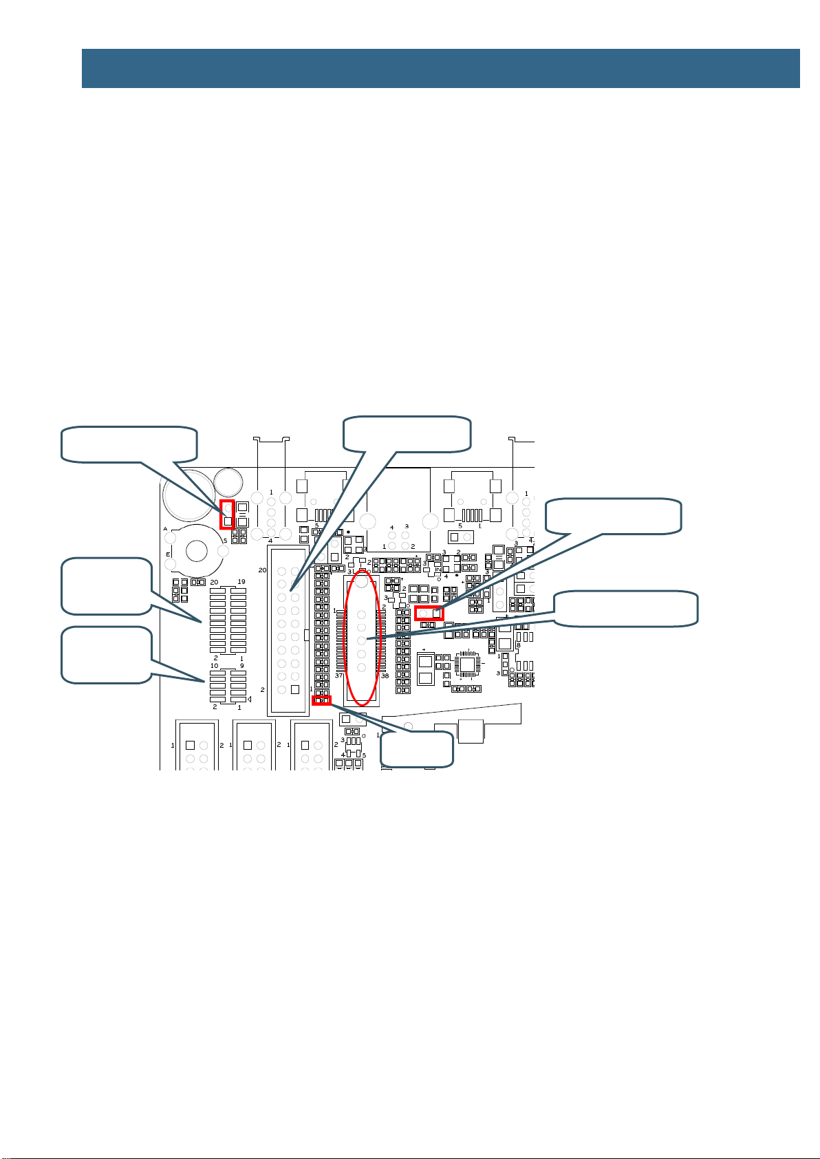
Slider switch JP1 is found on the top side of the LPC4357 OEM board, in the upper left corner.
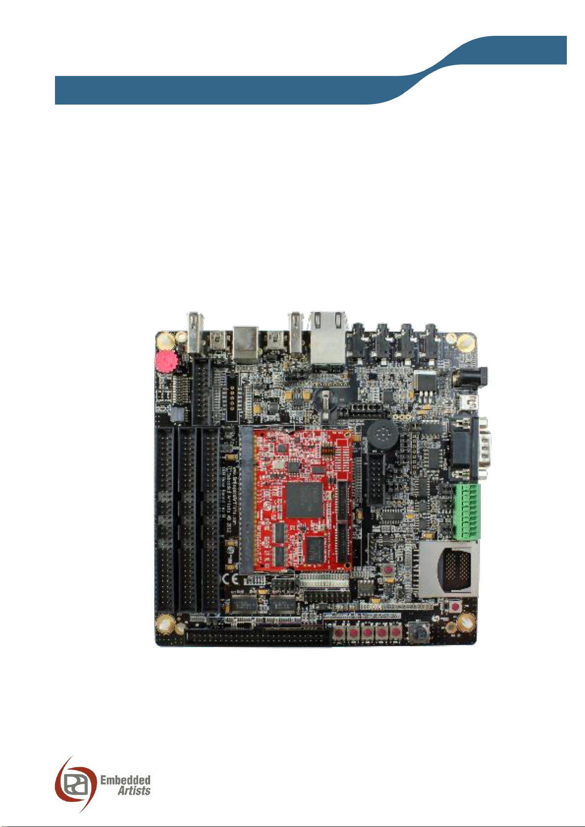
Figure 1 –LPC4357 OEM Board Picture, top side
J1
Trace connector
(Connector normally mounted)
JP1
From top to bottom;
BS0 setting
BS1 setting
BS2 setting
BS3 setting
0=’on’ pos, to the right
1=’off’ pos, to the left
J4 and J5
I2S, SGPIO and SCT expansion connectors
LED2
Memory card
interface powered

LPC4357 Developer’s Kit - User’s Guide
Page 12
Copyright 2013 © Embedded Artists AB
3.4 Trace Connector
There is a connector on the top side of the LPC4357 OEM board, carrying all signals needed for
debugging with trace. It is a standard 20 pos (50 mil pitch) trace connector as defined by ARM. Figure
1 illustrates where J1 is located on the board.
There is a trace connector on the OEM Base Board also, but this shall not be used for trace on the
LPC4357. It was not possible to get compatible pinning with other OEM boards. Instead J1 was added
to the design to support trace. Debugging without trace can be done either via J1 (on the LPC4357
OEM board) or the 10 pos debug connector (J7) on the OEM Base Board.
3.5 I2S and SGPIO Connectors
There are two 20-pos, 50 mil pitch connectors on the top side of the LPC4357 OEM board. See Figure
1 for location. These connectors carry selected I2S, I2C, SGPIO and SCT signals and can be used to
connect these signals to a separate expansion boards. For example an audio and video expansion
board. Note that some of the signals can be used on the OEM base board. Before using the signals,
always check for possible contentions.
3.6 uSD Memory Card Interface
There is a uSD/transflash memory card interface connector, J2, on the bottom side of the board. See
Figure 2 . LED2, on the top side, lights when the interface is powered. See Figure 1to locate LED2.
The signals on the SODIMM edge connector that are normally allocated for memory card interface (on
other OEM boards) carry other signals on the LPC4357 OEM board that have no relation to the
memory card interface.
Figure 2 –LPC4357 OEM Board Picture, bottom side
J2
uSD/transflash connector

LPC4357 Developer’s Kit - User’s Guide
Page 13
Copyright 2013 © Embedded Artists AB
3.7 Board Options
The schematic for the LPC4357 OEM Board show some different mounting options, mainly via SJx
jumpers but also some resistors that are not mounted per default. The design has been prepared for
customized versions for different needs.
3.8 1 kBit I2C E2PROM with EUI-48™ Number
The LPC4357 OEM Board contains a small E2PROM, 24AA02E48 from Microchip that can be
accessed via I2C. The chip contains a globally unique 48-bit number (EUI-48™) that can be used as
Ethernet MAC address. See the 24AA02E48 datasheet for details.
LPC4357 Developer’s Kit - User’s Guide
Page 14
Copyright 2013 © Embedded Artists AB
4 OEM Base Board Design
This chapter contains information about the peripherals and general design of the OEM Base Board
and how to set the different jumpers on the board. The schematic can be downloaded in pdf format
from the support page, and is recommended to have printed out while reading this chapter.
Section naming begins with SPx, which is short for Schematic Page x.
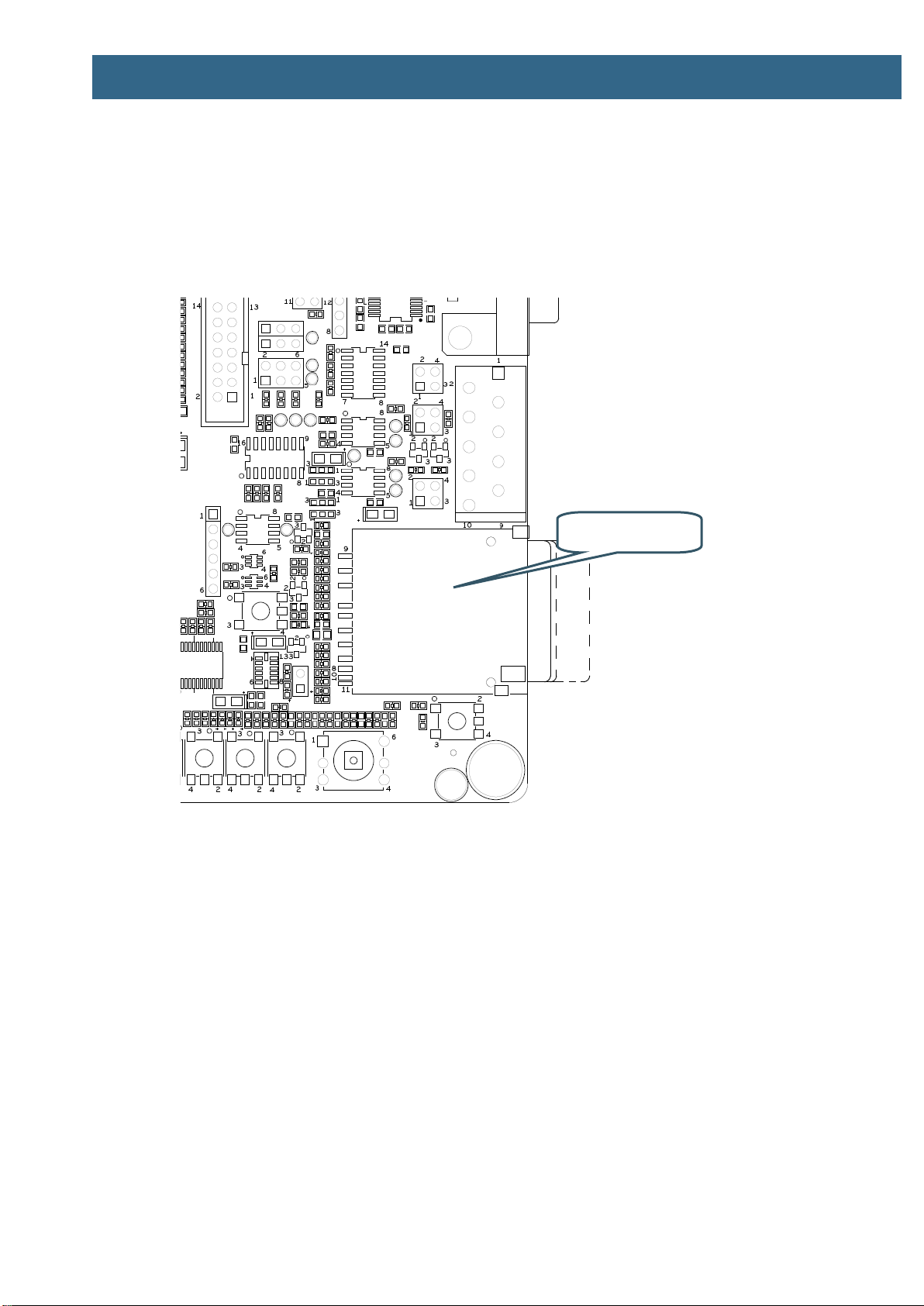
The picture below gives an overview of the OEM Base Board design.
Figure 3 –OEM Base Board Overview
4.1 Modifications to OEM Base Board
The OEM Base Board has been designed to be flexible. Most options can be controlled via jumpers
but some options might need soldering. Note that modifications to the board are done at own risk and
void all warranties.
Debug Connectors
Expansion
Connectors
LCD Expansion
Connector
OEM Board
Connector
Serial
Interfaces
Audio
Interfaces
USB
Interfaces
Ethernet
Interface
Power
Supply
SD/MMC
connector
Pushbuttons
and LEDs
Memory Bus
Expansion
RF module
interface
on solder
side
Reset Push-button
SW1

LPC4357 Developer’s Kit - User’s Guide
Page 15
Copyright 2013 © Embedded Artists AB
4.2 SP2: OEM Board Connector
The LPC4357 OEM board connector is a standard DDR2 SO-DIMM socket with 200 positions and
0.6mm pitch. It has 1.8V keying (which is what DDR2 stands for). The JEDEC standard defining the
DDR2 SODIMM boards is called JEDEC MO-224.
The signal names are general and represent the OEM base board functionality, rather than the
LPC4357 signal names. This is because the OEM base board also supports other OEM boards.
4.3 SP2: Current Measurements
It is possible to accurately measure current consumption of the LPC4357 OEM board. This can be very
valuable when working with applications that make use of the low power modes of the LPC4357
processors. The circuit is based on the chip ZXCT1010 from Diodes/Zetex. This chip generates a
voltage output proportional to the current through R2. This voltage can be measured over J2. 100mA
gives a 500mV output voltage, or expressed differently, 1mV correspond to 0.2mA
It is possible to remove R1, R2 and/or R3 for measuring current with an external multimeter. Note that
VCC_MAIN and VCC_BUFFERS are connected on the LPC4357 OEM board so there is no difference
between these supplies. This division has been done for compatibility with other OEM boards.
Figure 4 –Current Measurement J2
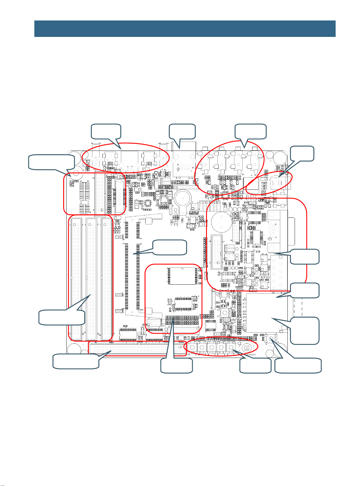
4.4 SP3: Expansion Connectors
All relevant OEM board signals are available for external use via three 64 pos IDC expansion
connectors; J3, J4 and J5. The expansion connectors are close to the SO-DIMM connectors to
minimize signal distortion.
Note that some OEM board circuits may need to be disconnected before externally used. Carefully
investigate the need for this before using a signal for external expansion.
Note that J4 has gathered all needed signals for expanding the memory bus (16-bit bus expansion). J4
is the expansion connector closest to the board edge. For 32-bit memory bus expansion, J3 is also
needed (for the upper 16 bits of the databus).
Current Measurement
J2 (left: signal, right: gnd)
LPC4357 Developer’s Kit - User’s Guide
Page 16
Copyright 2013 © Embedded Artists AB
Figure 5 –Expansion Connectors J3, J4, J5
4.5 SP4: External Memory Bus
This part of the OEM Base Board demonstrates how the external memory bus can be used for
expansion of custom circuits. Two different devices are connected to the memory bus; a 16-bit parallel
NOR flash and a 16-bit register.
In order to be universal between 16- and 32-bit databus width OEM Boards, only the lower 16 bits are
connected.
The 16-bit parallel NOR flash is enabled when JP1 is inserted, see picture below for guidance where to
find JP1 on the OEM Base Board. Note that the signal name is cryptic since the OEM Base Board is
compatible with many different OEM Board. For the LPC4357 OEM Board, the signal BCSY is actually
signal BCS0. This means that the NOR flash is accessible in memory region: 0x1C00 0000 - 0x1CFF
FFFF.
Also, a 16-bit register is connected to the external memory bus. The 16 bits in the register directly
drives 16 LEDs (a high signal light a LED). The signals are also available on an expansion connector
(J6). It can for example connect to a logic analyzer, for high-bandwidth logging. The upper and lower 8
bits are individually writeable. Signals BBLS0/BBLS1 controls the lower and upper 8 bits, respectively.
Since the OEM Base Board is universal and supports many different OEM Boards, the chip select
signal is either signal BCSX or GPIO69. For the LPC4357 OEM Board, the signal BCSX is actually
Expansion Connectors
left to right: J4, J3, J5

LPC4357 Developer’s Kit - User’s Guide
Page 17
Copyright 2013 © Embedded Artists AB
signal BCS2. This means that the register is accessible in memory region: 0x1E00 0000 - 0x1EFF
FFFF. No jumper in JP2 is needed when working with the LPC4357 OEM Board.
SJ12 shall be in default position (pad 1-2 shorted) to let BCS2 control chip select of the 16-bit register.
SJ1 controls the output enable of the register. By default it is grounded (pad 1-2 is shorted) and hence
the register drives the LEDs and expansion connector, J6.
Figure 6 –External Memory Bus Circuit
4.6 SP5: Debug Interfaces
Note that the LPC4357 MCU is sensitive to ESD on the JTAG port. Observe extra care around this.
Make sure the ground of the JTAG interface is connected to the OEM Base Board ground
before even connecting the JTAG interface. Never have the OEM Board unpowered while the
JTAG pod is powered.
The multiple debug interfaces can look complex, but that is just because the board supports many
different OEM Boards. The connectors are:
J7 –this is the new and smaller footprint standard ARM debug connector. It has 2x5 pins in
50 mil pitch. The connector supports both the SWD and JTAG interfaces. Note that not all,
and in particular older, JTAG debug probes do not support the SWD interface standard.
Note where pin 1 is found (see picture below) for this connector.
J8 –this is the old and big footprint standard ARM debug connector. It has 2x10 pins in 100
mil pitch. The connector supports both the SWD and JTAG interfaces. Note that not all, and in
particular older, JTAG debug probes do not support the SWD interface.
J9 –this is the old and big footprint 38 pin Mictor connector for ETM trace for the LPC2478.
This connector is not mounted. It is not used when working with the LPC4357 OEM board.
The connector can be soldered to the board if needed. The connector can be bought from
16-bit register
U2
Parallel NOR FLASH
U3
JP2 and JP1
left: JP2
right: JP1
LEDs
left to right: LED16 - LED 1
Register CS
control
SJ12
Register OE-
control
SJ1
LPC4357 Developer’s Kit - User’s Guide
Page 18
Copyright 2013 © Embedded Artists AB
Tyco Electronics Amp and is a 38-way receptacle Mictor connector, 0.025” pitch, part number:
767054-1 or 2-5767004-2 (RoHS compliant).
J10 –this is the new and smaller footprint standard ARM Cortex-M3/M4 connector for trace. It
carries the trace signals as well as the debug signals found on J7. Note that this connector
is not used when working with the LPC4357. Instead a 20 pos trace connector, J1,
exists on the LPC4357 OEM board itself.
When working with the LPC4357 OEM Board, J7 is typically used. If an older and big footprint JTAG
debug pod is used, J8 can alternatively be used.
If trace is also used, use the connector J1 on the LPC4357 OEM board. Note that this requires an
advanced JTAG probe that supports trace.
Note that JP4 shall be shorted in order to enable the JTAG/SWD interface on the LPC4357. JP4
might not be inserted by default on the OEM Base Board.
JP3 is not used for debug purposes when working with the LPC4357 OEM Board.
Figure 7 –Debug Interfaces
Trace&Debug Connectors
J9 –not used
Trace&Debug
Connectors
J10 –not used
Debug Connectors
J8
Debug
Connectors
J7
ETM Control Jumpers
JP3 –not used
Reset LED
LED17
Debug Control Jumpers
JP4

LPC4357 Developer’s Kit - User’s Guide
Page 19
Copyright 2013 © Embedded Artists AB
4.7 SP6: Ethernet Interface
The board has an Ethernet interface, J11, which is a RJ45 connector with integrated magnetics. There
is also provision on the board for connecting a PoE interface. All signals can be accessed via
expansion pads, J12. Five 0 ohm resistors have to be removed in that case for isolating J11 from the
new connector (this is because J11 is not capable of handling a PoE interface so a new RJ45
connector must added). See picture below for where to find the relevant components on the board.
Figure 8 –Debug Interfaces
PoE modules that can be used for testing can for example be found at
http://www.silvertel.com/poe_products.htm. Select a version delivering +5V with enough current
capability for the specific application in mind. For example, using USB Host with power hungry external
devices will require more current. In most situations a 9-10W module will be sufficient.
Besides the PoE module, a RJ45 capable of handling PoE is also needed.
PoE Connector
J12, pin 1 leftmost
Isolation Resistors
R51/52/53/56/57
RJ45 with Magnetics
J11
LPC4357 Developer’s Kit - User’s Guide
Page 20
Copyright 2013 © Embedded Artists AB
4.8 SP6: SD/MMC Memory Card Interface
The board has a SD/MMC memory card interface, J13. Note that this interface SHALL NOT be used
for accessing the MCI peripheral interface of the LPC4350. Instead, there is a uSD/transflash memory
card interface on the bottom side of the LPC4357 OEM board.
There is visual indication via LED2 on the LPC4357 OEM board that supply voltage to the memory
card is present.
Figure 9 –SD/MMC Memory Card Interface –Not used
SD/MMC Connector
J13 –not used
This manual suits for next models
13
Table of contents
Other Embedded Artists Microcontroller manuals

Embedded Artists
Embedded Artists LPC3152 User manual

Embedded Artists
Embedded Artists LPC1343 User manual

Embedded Artists
Embedded Artists iMX Series User manual

Embedded Artists
Embedded Artists iMX RT1052 User manual

Embedded Artists
Embedded Artists iMX RT1062 User manual

Embedded Artists
Embedded Artists LPC4357 User manual

Embedded Artists
Embedded Artists LPC3250 User manual

Embedded Artists
Embedded Artists LPC11U35 User manual

Embedded Artists
Embedded Artists LPC1343 User manual

Embedded Artists
Embedded Artists LPC3131 User manual


