Embedian MXM-6410 User manual

Computer on Module
COM Ports
Two USB Hosts
LCD
Ethernet
CompactFlash
MXM-6410 Firmware Restore Guide

Table of Contents
CHAPTER 1 SYSTEM INFORMATION............................................................................................4
1.1 STARTING EVKM-MXM-6410.......................................................................................................4
1.2 JUMPER SETTING ............................................................................................................................5
1.3 CONNECTORS................................................................................................................................10
CHAPTER 2 FIRMWAREARCHITECTURE.................................................................................13
2.1 FIRMWARE ....................................................................................................................................13
2.2 SWITCHING BOOT OPTION FROM NOR OR NAND.........................................................................13
2.3 FIRMWARE ARCHITECTURE IN NAND FLASH ...............................................................................15
CHAPTER 3 RESTORE THE FIRMWARE IN NAND FLASH.....................................................18
3.1 RESTORE STEPLDR AND EBOOTFROM NOR FLASH ....................................................................18
3.2 RESTORE NK IMAGE FROM EBOOT.............................................................................................28
3.3 RESTORE FIRMWARE IN NAND FLASH FROM SD BOOT ................................................................34
3.3.1. Using PC Tool to Fusing the SD/SDHC card......................................................................34
3.3.2. Using SD boot fusing NAND flash......................................................................................35

System Information
This Chapter gives an introduction of system information
to let users quickly pick up how to setting up the system.
Section include:
zSystem Setup
zJumper Setting
zFirmware architecture in NAND flash

Chapter 1 System Information
This Chapter gives an introduction of hardware information so that users can
quickly set up the system.
1.1 Starting EVKM-MXM-6410
Before starting, please check the jumper to make sure that the jumper
configuration is matching your demand. Figure 1.1 shows the steps.
Figure 1.1 Starting EVKM-MXM-6410
1. Press the MXM-6410 module and screw it tightly.
2. Connect the console port (UART0, CN20 on figure 1.3) to the console
cable, then to a null modem cable and then connect to your PC. Open
up the DNW 0.6c (Click “Connect” at “Serial Port” tab) and set the
baud rate to 115200, 8N1, no hardware flow control. (At
“Configuration” Tab Æ“Options” of DNW program serial port setting.)
3. Connect the backlight invert board power to CN9.
4. Connect the LCD FPC Cable (Top Contact) or LVDS cable.
5. Connect the power cable to power board.

1.2 Jumper Setting
This section gives details of the hardware features of the EVKM-MXM-6410.
These include a description of the switches, jumper settings, connectors and
connector pin outs.
Jumpers
The EVKM-MXM-6410 SBC has a number of jumpers that allow you to
configure your system to suit your application. All use 2mm shorting blocks
(shunts) to select settings. Turn off power of the EVKM-MXM-6410 before
changing the position of a shunt.
Jumper Location
Figure 1.2 Jumper Location

List of Jumpers
The table below lists the function of various jumpers.
Table 1.1 Jumpers
Table 1.1 Jumpers
Label Function
JP1 NOR boot or NAND boot Setting and LCD Scan Direction
Setting
JP2 LCD Power Setting (3.3V or 5V for both TTL and LVDS)
JP3 RS232/422/485 Setting

S1 Reset Button
Jumper Settings
The following tables describe how the jumper shunts to various configurations.
JP1: Location on Board, D1
Table 1.2 NOR Boot or NAND Boot and LCD Scan Direction Setting (JP1)
Table 1.2 NOR Boot or NAND Boot and LCD Scan Direction
Setting
Setting Function
N.C.(Default) NAND Boot
JP1 (1-2) NOR Boot
JP1 (3-4) Pull-High of CN14 Pin 30
JP1 (5-6) Pull-High of CN14 Pin 31
JP2: Location on Board, C1
Table 1.3 LCD VCC Power Setting for CN14 and CN15 (JP2) (from CPU
LVDS and TTL)
Table 1.3 LCD VCC Power Setting for CN14 (JP2) (from CPU LVDS
and TTL)
Setting Function
JP2(1-2)(Default) 3.3V
JP2(3-4) 5V
JP3: Location on Board, B6
Table 1.4 RS232/422/485 Mode Setting
Table 1.4 RS232/422/485 Setting
Setting Function
JP3(1-2)(Default) RS232
JP3(3-4) RS422/RS485 half duplex
JP3(5-6) RS422/RS485 full duplex

Note: If JP3 jumper set to be RS232, the RS232 connector will be CN20
(UART1) header. If JP3 jumper set to be RS422 and RS485, the connector will
be CN22 header. User can only choose one (RS232 or RS422 or RS485) at
the same time.
S1: Location on Board, D6
Table 1.5 Reset Button
Table 1.5 Reset Button
Setting Function
Press Button and
Release Immediately Reset CPU and IO
Setting Jumpers
You configure your board to match the needs of your application by setting
jumpers. A jumper is the simplest kind of electric switch. It consists of two
metal pins and a small metal clip (often protected by a plastic cover) that slides
over the pins to connect them. To "close" a jumper you connect the pins with
the clip.
To "open" a jumper you remove the clip. Sometimes a jumper will have three
pins, labeled 1, 2 and 3. In this case you would connect either pins 1 and 2 or 2
and 3.
The jumper settings are schematically depicted in this manual as follows.

A pair of needle-nose pliers may be helpful when working with jumpers. If you
have any doubts about the best hardware configuration for your application,
contact your local distributor or sales representative before you make any
change.
Generally, you simply need a standard cable to make most connections.

1.3 Connectors
Onboard connectors link the EVKM-MXM-6410 to external devices such as
LCD panel, a keyboard, an audio headset or CompactFlash and to external
communication such as 802.11, USB or Ethernet link. The table below lists the
function of each of the board’s connectors.
Connector Location
Figure 1.3 Connector Location

List of Connectors
Table 1.6 List of Connectors
Table 1.6 Connector
Label Function
CN5 JTAG
CN6 CF Type I/II Connector
CN7 SATA Connector
CN8 Power Connector
CN9 LCD Backlight Inverter Connector
CN10 RTC Battery Connector
CN11 Audio (Microphone in, Headphone out, Line in) Connector
CN12 Buzzer
CN13 S-Video and CVBS Video Connector
CN14 TTL Level LCD FPC Connector
CN15 LVDS LCD Connector
CN16 VGA DSub-15 Connector
CN17 Ethernet RJ45 and Double USB Host Type A Connector
CN18 Double USB Host Header
CN19 USB OTG Type B Connector
CN20 UART 0 and UART 1 Header
CN21 UART 2 and UART 3 Header
CN22 SPI and RS422/485 Header
CN23 UART 4 and UART 5 Header
CN24 SD/SDHC Connector
CN25 GPIO Header
CN26 4-Wire Touch Panel Connector
CN27 CAN Bus Connector
.

Firmware Architecture
This Chapter gives background information on the
firmware architecture of MXM-6410 computer on module.
Section include:
zFirmware
zSwitching boot option from NOR or NAND
zFirmware architecture in NAND flash

Chapter 2 Firmware Architecture
This Chapter gives an overall picture in regarding to the firmware architecture
of MXM-6410 computer on module. This helps users understand what they are
doing when upgrade or restore the firmware.
2.1 Firmware
There are NOR flash (on carrier board) and NAND flash (on the module) reside
in the system and play different roles. The firmware in NAND includes
stepldr.nb0 (BootStrap Loader), eboot.bin and NK.bin. The system is booting
from NAND flash by default. The firmware in NOR flash will not be used during
normal operation. It stores some utilities like writing MAC address, checking
bad blocks of NAND flash or restoring/upgrading the firmware to NAND when
the eboot is gone for somehow. The firmware restoring is especially important
in this kind of NAND boot device. All firmware will be factory pre-loaded.
2.2 Switching boot option from NOR or NAND
The NAND boot or NOR boot is determined by JP1 jumper setting on
Embedian 3.5-inch APC-6410 series single board computers. The default
setting (JP1 1-2 open) is NAND boot. And shunt the 1-2 of JP1 will switch to
NOR boot. Always power off when changing the jumpers.

Following figure shows the jumper setting of NAND boot and NOR boot.
Figure 2.1 Jumper Settings of NOR Boot and NAND Boot

2.3 Firmware Architecture in NAND flash
Figure 2.2 shows the firmware architecture in NAND flash.
Figure 2.2 Firmware Architecture in NAND Flash
When power on, the processor will copy the first 4K of BootStrap Loader
(stepldr.nb0) to internal RAM. The stepldr will initialize the memory mapping
and load the eboot from the 2nd block (0x2, 1 block = 128K) of NAND flash.
The WinCE 6.0 kernel (NK.bin) starts from the 6th block (0x6). There are about
97.5MB un-used in NAND for users. User can see the flash information at My
Device\NandFlash when booting up. Click the mouse or touch on the icon for a
few seconds and Tab the “Properties” as Figure 2.3.

Figure 2.3 Flash Information
The purposes of this document are to tell users how to restore or upgrade the
firmware in NAND flash. The next chapter will detail that.

Restore the Firmware
in NAND flash
This Chapter details how to restore the firmware in NAND
flash of MXM-6410 computer on module.
Section include:
zRestore Stepldr.nb0 and EBOOT.bin from NOR flash
zRestore NK image from EBOOT
zRestore firmware in NAND flash from SD boot

Chapter 3 Restore the firmware in
NAND flash
This chapter first gives two steps to restore the firmware in NAND flash. If the
EBOOT of the system is gone, users need to follow the “Restore Stepldr.nb0
and EBOOT.bin from NOR flash “ that described in section 3.1. If the EBOOT
of the system is still alive, users can go to the section 3.2 directly. And in the
last section of this chapter, we will introduce how to restore the firmware in
NAND flash from SD boot.
Before going on, users need to install two kinds of USB drivers that Embedian
provided with on your Windows PC first. The “secusb2” is for the USB
download during the NOR boot configuration and the “wceusbsh” is the
Windows CE USB RNDIS driver. (When plug the USB cable to the Windows
PC at first time, Windows will ask you to install the driver. Just point to the
directory where your USB driver placed and the installation will be done.)
3.1 Restore Stepldr and EBOOT from NOR flash
User will need this chapter in case that your EBOOT is erased by accident or
gone for somehow. To write Stepldr and EBOOT images to NAND flash using
NOR boot, first, power off device and set the jumper JP1 to NOR flash
configuration. (Be sure to power off the system before you changing the
jumper.)
Install the USB host driver to your Windows system and DNW v0.6C programs
that Embedian provided in your host Windows PC. Connect the serial console
cable from serial console port (UART 0 in CN20 of Embedian SBC) of device
to the COM port of your Windows PC. And connect a USB cable from USB
device port (CN19 of Embedian SBC) to USB host port of your Windows PC.
In "Serial Port" of your dnw program, click on "Connect" and power on device.
In "Configuration" of dnw program, at "Options" set the COM port as the
following setting of figure 3.1. And the USB Port Download Address is
"0x50030000", this is the DDR DRAM address where the program will be
executed. The baud rate is 115200 and the host COM port is this example is
"COM 1"

Figure 3.1 COM and USB Port Setting of DNW Program

Step 1
Power on the device and you should see the following screen in your DNW
programs as shown in figure 3.2.
Figure 3.2 NOR Boot Splash Screen
Table of contents
Other Embedian Single Board Computer manuals
Popular Single Board Computer manuals by other brands
Asus
Asus Aaeon RICO-3288 user manual
Silicon Laboratories
Silicon Laboratories TOOLSTICK C8051F330 manual
SolidRun
SolidRun ClearFog user manual
Teknor Industrial Computers
Teknor Industrial Computers VIPer808 Technical reference manual
Advantech
Advantech ROM-5620 user manual
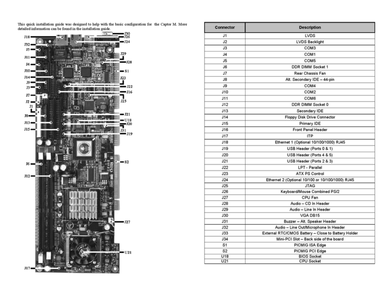
Corvalent
Corvalent Captor M Quick installation guide
