Endace DAG 3.8S User manual

DAG 3.8S Card User Guide
EDM01-09

EDM01-09v15 DAG_3.8S_Card_User_Guide
©2005 - 2008 Endace Technology Ltd. Confidential - Version 14 - June 2008
Protection Against Harmful Interference
When present on equipment this manual pertains to, the statement "This device complies with part 15 of the FCC
rules" specifies the equipment has been tested and found to comply with the limits for a Class A digital device,
pursuant to Part 15 of the Federal Communications Commission [FCC] Rules.
These limits are designed to provide reasonable protection against harmful interference when the equipment is
operated in a commercial environment.
This equipment generates, uses, and can radiate radio frequency energy and, if not installed and used in
accordance with the instruction manual, may cause harmful interference to radio communications.
Operation of this equipment in a residential area is likely to cause harmful interference in which case the user will
be required to correct the interference at their own expense.
Extra Components and Materials
The product that this manual pertains to may include extra components and materials that are not essential to its
basic operation, but are necessary to ensure compliance to the product standards required by the United States
Federal Communications Commission, and the European EMC Directive. Modification or removal of these
components and/or materials, is liable to cause non compliance to these standards, and in doing so invalidate the
user’s right to operate this equipment in a Class A industrial environment.
Disclaimer
Whilst every effort has been made to ensure accuracy, neither Endace Technology Limited nor any employee of
the company, shall be liable on any ground whatsoever to any party in respect of decisions or actions they may
make as a result of using this information.
Endace Technology Limited has taken great effort to verify the accuracy of this manual, but nothing herein should
be construed as a warranty and Endace shall not be liable for technical or editorial errors or omissions contained
herein.
In accordance with the Endace Technology Limited policy of continuing development, the information contained
herein is subject to change without notice.
Website
Copyright 2005 - 2008 Endace Technology Ltd. All rights reserved.
http://www.endace.com
No part of this publication may be reproduced, stored in a retrieval system, or transmitted, in any form or by any
means electronic, mechanical, photocopying, recording, or otherwise, without the prior written permission of the
Endace Technology Limited.
Endace, the Endace logo, Endace Accelerated, DAG, NinjaBox and NinjaProbe are trademarks or registered
trademarks in New Zealand, or other countries, of Endace Technology Limited. Applied Watch and the Applied
Watch logo are registered trademarks of Applied Watch Technologies LLC in the USA. All other product or
service names are the property of their respective owners. Product and company names used are for identification
purposes only and such use does not imply any agreement between Endace and any named company, or any
sponsorship or endorsement by any named company.
Use of the Endace products described in this document is subject to the Endace Terms of Trade and the Endace
End User License Agreement (EULA).

EDM01-09v15 DAG_3.8S_Card_User_Guide
©2005 - 2008 Endace Technology Ltd. Confidential - Version 14 - June 2008 i
Contents
Introduction 1
Overview .....................................................................................................................................................................1
Card Features..............................................................................................................................................................1
Purpose of this User Guide ....................................................................................................................................... 2
System Requirements................................................................................................................................................. 2
General ...................................................................................................................................................................2
Operating System ................................................................................................................................................. 2
Other Systems........................................................................................................................................................ 2
Card Description ........................................................................................................................................................ 3
Fixed optical transceiver version ........................................................................................................................ 3
Pluggable optical transceiver version ................................................................................................................3
Battery removal – don’t do it! .............................................................................................................................4
Card Architecture.......................................................................................................................................................4
Line Types ................................................................................................................................................................... 5
Supported Line Types ..........................................................................................................................................5
Extended Functions....................................................................................................................................................6
Co-Processor..........................................................................................................................................................6
Inline Forwarding ................................................................................................................................................. 6
Installation 7
Introduction ................................................................................................................................................................7
DAG Software package .............................................................................................................................................7
Inserting the DAG Card ............................................................................................................................................7
Port Connectors .......................................................................................................................................................... 8
Fixed optical transceivers version ...................................................................................................................... 8
Pluggable optical transceiver version ................................................................................................................8
Fixed Optical Transceivers ........................................................................................................................................9
Optical modules .................................................................................................................................................... 9
Pluggable Optical Transceivers .............................................................................................................................. 10
Overview.............................................................................................................................................................. 10
Optical modules .................................................................................................................................................. 10
Power Input ......................................................................................................................................................... 11
Splitter Losses...................................................................................................................................................... 11
Configuring the DAG card 13
Introduction .............................................................................................................................................................. 13
Before configuring the DAG card..................................................................................................................... 13
Firmware images ................................................................................................................................................ 13
Setting up the FPGA ................................................................................................................................................ 14
Programming the FPGA .................................................................................................................................... 15
dagrom ................................................................................................................................................................. 16
dagld..................................................................................................................................................................... 17
Loading new firmware images onto a DAG Card ......................................................................................... 17
Preparing the DAG card for use............................................................................................................................. 17
Configuring the DAG card...................................................................................................................................... 18
Display Current Configuration......................................................................................................................... 18
dagconfig tokens explained............................................................................................................................... 19
dagconfig options ............................................................................................................................................... 26
dagthree options ................................................................................................................................................. 28
Viewing the DAG card status ................................................................................................................................. 29
Interface Status.................................................................................................................................................... 29
Port Statistics ....................................................................................................................................................... 30
Status Bits............................................................................................................................................................. 31
ATM Network ..................................................................................................................................................... 31
PoS Network........................................................................................................................................................ 31

EDM01-09v15 DAG_3.8S_Card_User_Guide
ii ©2005 - 2008 Endace Technology Ltd. Confidential - Version 14 - June 2008
Verify Configuration.......................................................................................................................................... 31
General Purpose Counters ................................................................................................................................ 32
Links Data and Cells .......................................................................................................................................... 32
Using your DAG card to capture data 33
Introduction .............................................................................................................................................................. 33
Basic data capture .................................................................................................................................................... 33
Starting a capture session .................................................................................................................................. 33
dagsnap................................................................................................................................................................ 34
Capturing data at high speed ........................................................................................................................... 35
Viewing captured data ............................................................................................................................................ 36
dagbits.................................................................................................................................................................. 36
Converting captured data....................................................................................................................................... 38
Dagconvert .......................................................................................................................................................... 39
Using third party applications ............................................................................................................................... 40
Transmitting captured data .................................................................................................................................... 40
Configuration...................................................................................................................................................... 40
Explicit Packet Transmission ............................................................................................................................ 40
Trace Files............................................................................................................................................................ 41
Synchronizing Clock Time 43
Overview................................................................................................................................................................... 43
DUCK Configuration............................................................................................................................................... 43
Common Synchronization ...................................................................................................................................... 43
Network Time Protocol........................................................................................................................................... 44
Timestamps............................................................................................................................................................... 45
Example ............................................................................................................................................................... 45
Dagclock .................................................................................................................................................................... 46
Dagclock Statistics reset..................................................................................................................................... 47
Dagclock output explained ............................................................................................................................... 48
Card with Reference ................................................................................................................................................ 50
Overview ............................................................................................................................................................. 50
Pulse Signal from External Source ................................................................................................................... 50
Connecting the Time Distribution Server ....................................................................................................... 50
Testing the Signal ............................................................................................................................................... 50
Single Card No Reference....................................................................................................................................... 51
Two Cards No Reference ........................................................................................................................................ 52
Overview ............................................................................................................................................................. 52
Synchronizing with Each Other ....................................................................................................................... 52
Synchronizing with Host................................................................................................................................... 53
Connector Pin-outs .................................................................................................................................................. 54
Overview ............................................................................................................................................................. 54
Pin Assignments ................................................................................................................................................. 54
Data Formats 55
Overview................................................................................................................................................................... 55
Generic ERF Header ................................................................................................................................................ 56
ERF 1. TYPE_POS_HDLC....................................................................................................................................... 58
ERF 3. TYPE_ATM................................................................................................................................................... 59
ERF 4. TYPE_AAL5.................................................................................................................................................. 60
ERF 10. TYPE_COLOR_HDLC_POS..................................................................................................................... 61
Extension Headers (EH).......................................................................................................................................... 62
Introduction ........................................................................................................................................................ 62
Troubleshooting 63
Reporting Problems ................................................................................................................................................. 63
Version History 65

EDM01-09v15 DAG_3.8S_Card_User_Guide
©2005 - 2008 Endace Technology Ltd. Confidential - Version 14 - June 2008 1
Introduction
Overview
The Endace DAG 3.8S card provides the means to transfer data at the full speed of the
network into the memory of the host computer, with zero packet loss, in even worst-case
conditions. Further, unlike a Network Interface Card (NIC), Endace products actively
manage the movement of network data into memory while only consuming a minimal
amount of the host computer's resources. The full attention of the CPU remains focused on
the analysis of incoming data without a constant stream of interruptions as new packets
arrive from the network. For a busy network link, this feature has a turbo-charging effect
similar to that of adding a second CPU to the system.
The DAG 3.8S is a two port, PCIx card that allows capture and transmission of data. It
supports packet and cell capture and transmit applications for OC3c or OC12c, ATM or
Packet-over-SONET (PoS) networks. The DAG 3.8S has two transceivers which can be
operated simultaneously allowing a single card to monitor one or both directions of a full-
duplex link. An optional Co-Processor daughter card can be added for enhanced filtering.
Card Features
The following features are available on this DAG card. Note: Different firmware images
may be required. Not all features are available on each firmware image. For further
information on which feature is available in what firmware image, see Firmware images
13
(page ).
•OC3 / STM-1 and OC12c / STM-4c
•ATM
•TERF
•Co-Processor based IPF (If Co-Processor fitted.)
•Co-Processor based AAL5 (If Co-Processor fitted.)

EDM01-09v15 DAG_3.8S_Card_User_Guide
2 ©2005 - 2008 Endace Technology Ltd. Confidential - Version 14 - June 2008
Purpose of this User Guide
The purpose of this User Guide is to provide you with an understanding of the DAG 3.8S
card architecture, functionality and to guide you through the following:
•Installing the card and associated software and firmware
•Configuring the card for your specific network requirements
•Running a data capture session
•Synchronizing clock time
•Data formats
You can also find additional information relating to functions and features of the DAG 3.8S
card in the following documents which are available from the Support section of the Endace
website at http://www.endace.com
•EDM02-02 Co-Processor IP Filtering Software Manual
:
•EDM04-01 DAG Software Installation Guide
•EDM04-03 dagflood User Manual
•EDM04-04 dagfwddemo User Guide
•EDM04-06 Daggen User Guide
•EDM04-08 Configuration and Status API Programming Guide
•EDM04-19 DAG Programming Guide
•EDM05-01 Time Distribution Server User Guide
•EDM11-01 ERF types
•PN01-13 DAG Card Quick Start Guide
This User Guide and the EDM04-01 DAG Software Installation Guide are also available in PDF
format on the installation CD shipped with your DAG 3.8S card.
System Requirements
General
The minimum system requirements for the DAG 3.8S card are:
•A computer, with at least a Intel Xeon 1.8GHz or faster and a minimum of 1GB RAM.
•At least one free PCI-X slot supporting 66MHz operation..
•Software distribution requires 60MB free space.
•For details of the supported operating systems, see one of the following documents:
•EDM04-01 DAG Software Installation Guide
•Current release notes - See the Documentation CD or the Endace support website
at https://www.endace.com/support
.
Operating System
This document assumes you are installing the DAG 3.8S card in a computer which already
has an operating system installed. To install refer to EDM04-01 DAG Software Installation
Guide. All related documentation is included on the CD shipped with the DAG 3.8S card.
Other Systems
For advice on using an operating system that is substantially different from any of those

EDM01-09v15 DAG_3.8S_Card_User_Guide
©2005 - 2008 Endace Technology Ltd. Confidential - Version 14 - June 2008 3
Card Description
The DAG 3.8S card standard configuration supports receive-only packet and cell capture
applications for OC3c or OC12c, ATM or Packet-over-SONET (PoS) networks.
The DAG 3.8S card has two transceivers which can be operated simultaneously allowing a
single card to monitor one or both directions of a full-duplex link.
The DAG 3.8S card is also capable of transmitting packets at 100% line rate on both ports
while simultaneously receiving packets at 100% line rate on both ports.
Older versions of the DAG 3.8S card use standard fixed optical transceivers while newer
versions (Rev G onwards) have pluggable optical transceivers.
Both versions are shown next.
Fixed optical transceiver version
Pluggable optical transceiver version
EDM01-09v15 DAG_3.8S_Card_User_Guide
4 ©2005 - 2008 Endace Technology Ltd. Confidential - Version 14 - June 2008
Battery removal – don’t do it!
Removing the battery from a DAG card voids your warranty.
Removing the battery from a DAG card will cause the loss of encryption key used to decode
the DAG card's firmware. Once the encryption key is lost the DAG card must be returned to
Endace for reprogramming.
The battery in this product is expected to last a minimum of 10 years.
Caution
Risk of explosion if the battery is replaced by an incorrect type.
Dispose of used batteries carefully.
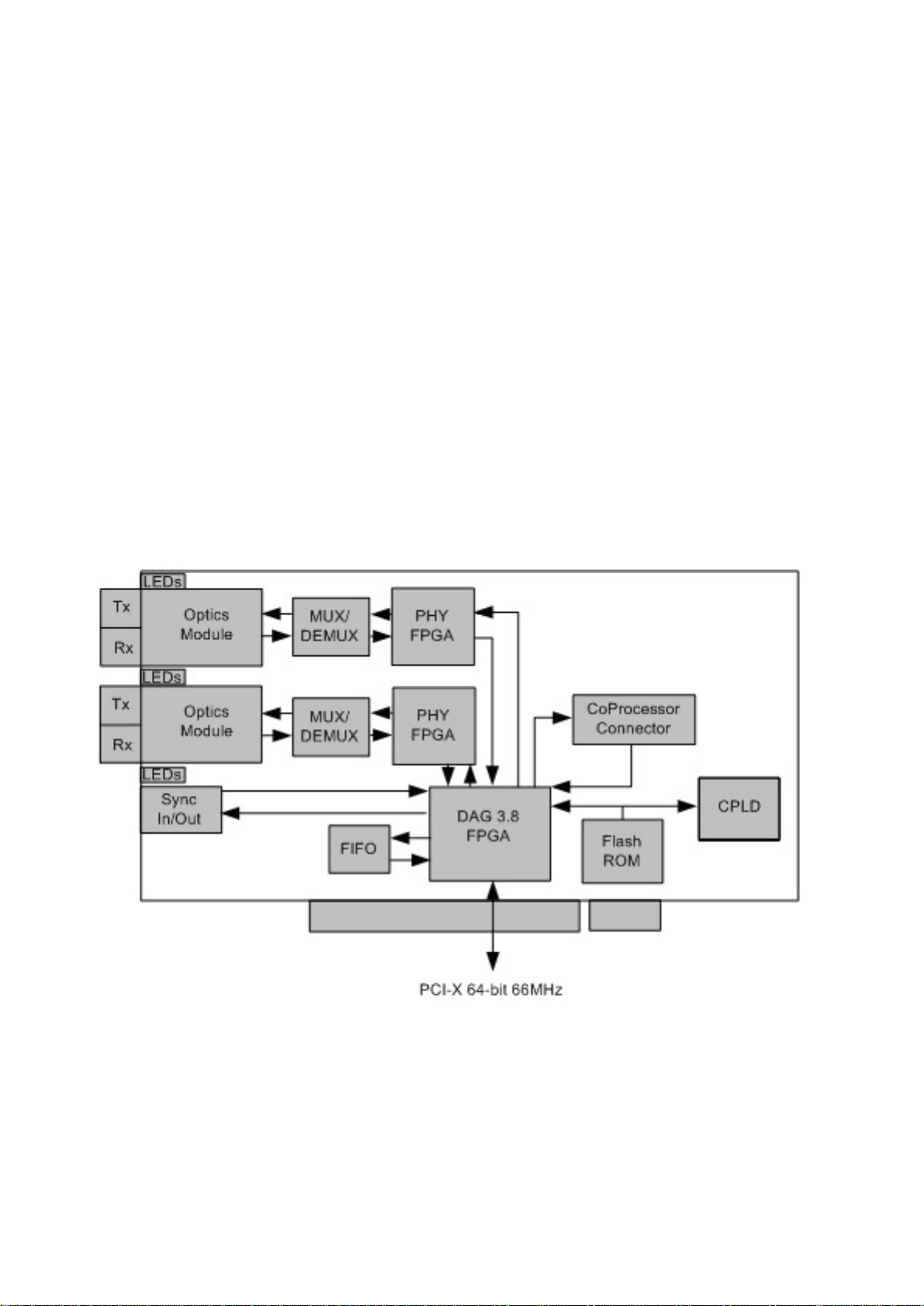
Card Architecture
Serial SONET/SDH optical data is received by two optical interfaces, and passed through de-
multiplexers. The network data feeds immediately into two physical layer FPGAs.
The SONET/SDH payload data is then sent to the main FPGA. This FPGA contains the
DUCK timestamp engine, packet record processor, and PCI-X interface logic.
Because of component close association, packets or cells are time-stamped accurately. Time
stamped packet records are stored in an external FIFO before transmission to the host.
The diagram below shows the DAG 3.8S card's major components and flow of data:
EDM01-09v15 DAG_3.8S_Card_User_Guide
©2005 - 2008 Endace Technology Ltd. Confidential - Version 14 - June 2008 5
Line Types
It is important that you understand the physical characteristics of the network to which you
want to connect. If your configuration settings do not match your network, the DAG 3.8S
card will not function as expected.
Note: If you are unsure about which of the options listed below to apply to your network,
please contact your Network Administrator for further information.
Supported Line Types
The line characteristics supported by the DAG 3.8S card are described below.
Type Description
PoS/ATM Packet over SONET/Asynchronous Transfer Mode.
OC-3/OC-3c
A SONET network line with transmission speeds up to 155.52 Mbit/s using
fiber optics. Also called STM-1 (SDH).
OC-12/OC-12c A SONET network line with transmission speeds up to 622.08 Mbit/s using
fiber optics. Also called STM-4 (SDH).

EDM01-09v15 DAG_3.8S_Card_User_Guide
6 ©2005 - 2008 Endace Technology Ltd. Confidential - Version 14 - June 2008
Extended Functions
Co-Processor
The DAG 3.8S card is equipped with a Co-Processor connector which can be used with the
optional Endace DAG Co-Processor as a data processing tool.
The specifications for the Co-Processor IP filtering/packet classification are:
•Packets are classified by TCP/IP header fields and/or payload content.
•Up to 16,384 TCP/IP header classification rules.
•Classification rules are assigned a user-defined 16-bit identifier
•Packets matching classification rules are assigned the matching rule's identifier.
•Programmable actions may be associated with each rule identifier. For example, The
packet should either be dropped, or presented to the host.
•Packets presented to the host include the rule-match identifier in the record header.
The specifications for the coprocessor ATM AAL5 Reassembler are:
•Supports up to 65,536 simultaneously active VCI/VPI's
•Supports simultaneous reassembly of up to 65,536 AAL5 frames
•Selected VPI/VCI discovery, state management, and ageing
•Supports up to full OC-12/STM-4 cell rate on both interfaces simultaneously [~2.8
Mcells/sec]
•Rich statistics, counters, and timeouts.
Inline Forwarding
for more information on
DAG coprocessor purchasing and pricing details.
The DAG 3.8S card supports inline forwarding which enables the card to receive and
transmit packets directly from a single memory. This allows you to forward packets from the
DAG card receive interface(s) to the DAG cards transmit interface(s) without the requirement
to copy them. Using inline forwarding you can receive, inspect, filter and forward packets
between ports.
dagfwddemo which is a tool supplied with your DAG card demonstrates how you can apply a
user-defined BSD Packet Filter (BPF) to the traffic forwarded by the DAG card. Packets
which match the filter are forwarded, while packets that do not match are dropped.
For more detailed information on inline forwarding and using dagfwddemo please refer to the
EDM04-04 dagfwddemo User Guide available from the support section of the Endace website
at http://www.endace.com
.

EDM01-09v15 DAG_3.8S_Card_User_Guide
©2005 - 2008 Endace Technology Ltd. Confidential - Version 14 - June 2008 7
Installation
Introduction
The DAG 3.8S card can be installed in any free PCIx slot. It operates at 66MHz in PCIx mode
but will not operate in 32-bit or 64-bit PCI slots.
Although the DAG driver supports up to sixteen DAG cards in one system, the DAG card
makes heavy use of PCIx bus data transfer resources. Therefore bandwidth limitations mean
you should not have more than one card on a single PCIx bus.
DAG Software package
The latest DAG Software package must be installed before you install the DAG 3.8S card
itself. See EDM04-01 DAG Software Installation Guide, which is included on the CD shipped
with the DAG 3.8S card.
Inserting the DAG Card
Caution:
It is very important to protect both the computer and the DAG 3.8S card from
damage by electro-static discharge (ESD). Failure to do so could cause damage to
components and subsequently cause the card to partially or completely fail.
1. Turn power to the computer OFF.
2. Remove the PCIx bus slot screw and cover.
3. Using an approved ESD protection device attach the end with the strap to your wrist
and pull or clip firmly so there is firm contact with your wrist.
4. Securely attach the clip on the other end of the strap to a solid metal area on the
computer chassis as shown below.
5. Insert the DAG 3.8S card into PCIx bus slot ensuring it is firmly seated.
6. If this DAG card requires an external power supply, complete the following steps:
a. Connect the supplied (or equivalent) power cable to the external power connector
on the DAG card.
b. Connect the cable to the appropriate power connector on your server's power
supply unit.
7. Check the free end of the card fits securely into the card-end bracket that supports the
weight of the card.
8. Secure the card with the bus slot cover screw.
9. Turn power to the computer ON.
10. Ensure the blue (FPGA successfully programmed) LED on the DAG card illuminates.

EDM01-09v15 DAG_3.8S_Card_User_Guide
8 ©2005 - 2008 Endace Technology Ltd. Confidential - Version 14 - June 2008
Port Connectors
The DAG 3.8S card has two socket connectors with each consisting of an optical fiber
transmitter and receiver.
•On Fixed optical transceiver versions of the card (pre-Rev G) these connectors are
fixed (1x9 optics with SC connector).
•In pluggable optical transceiver versions (Rev G onwards) they are pluggable (Small
Form Factor Pluggable (SFP)) with LC connector.
The upper connector of each pair is used for the transmit signal and the bottom connector of
each pair is used for the received signal.
The DAG 3.8S also has an 8-pin RJ45 PPS input socket located below the optical port
connectors on the card bracket. This is available for connection to an external time
synchronization source.
Caution: Never connect an Ethernet network or telephone line to the RJ-45 PPS input
socket.
Fixed optical transceivers version
Pluggable optical transceiver version

EDM01-09v15 DAG_3.8S_Card_User_Guide
©2005 - 2008 Endace Technology Ltd. Confidential - Version 14 - June 2008 9
Fixed Optical Transceivers
Fixed optical transceiver versions (pre Rev G) of the DAG 3.8S are shipped with the 1x9
optics module fitted. If you wish to use a different module you must specify this at the time
of ordering.
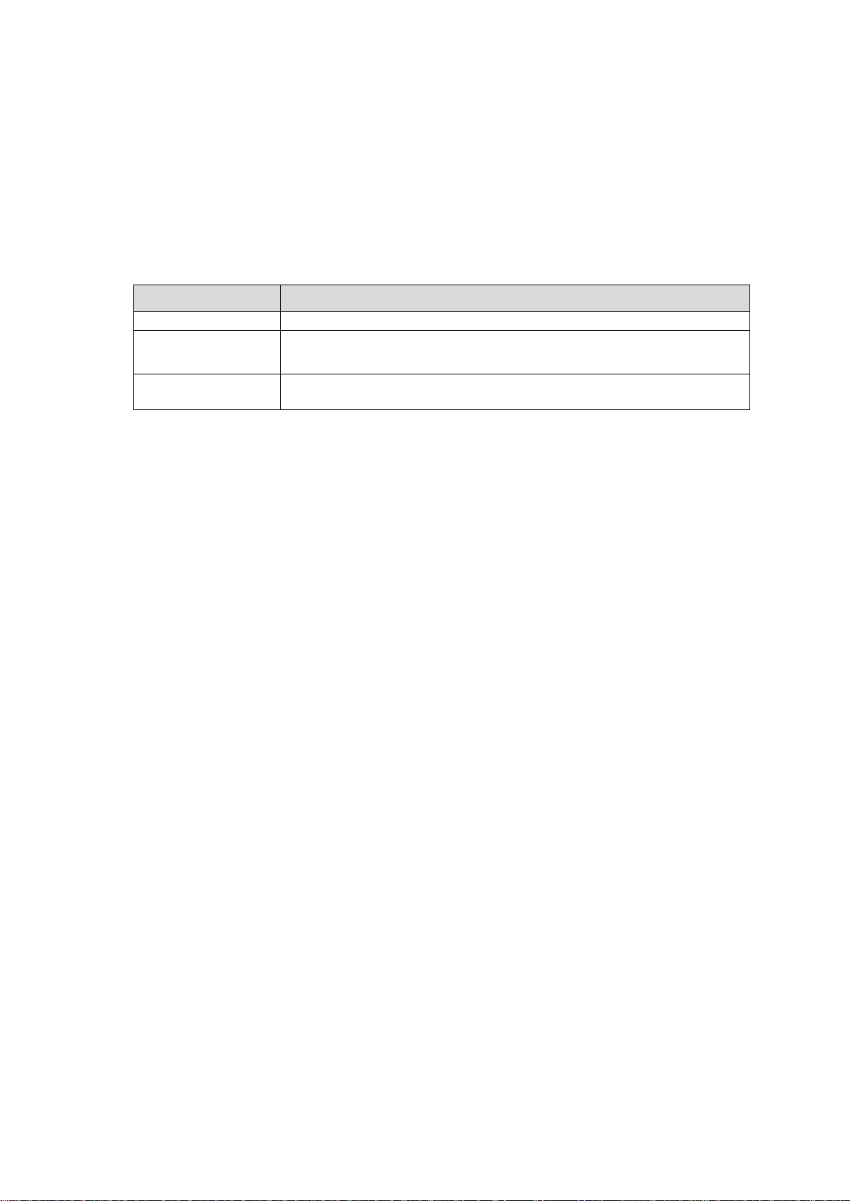
Optical modules
The optical power range depends on the particular module that is fitted to the DAG 3.8S
card. Optics modules are supplied in either Single or Multi mode. See the following table for
details.
Optical power is measured in dBm. This is decibels relative to 1 mW where 10 dB is
equivalent to a factor of 10 in power. A negative optical power value indicates power that is
less than 1 mW. The most sensitive devices can work at power levels down as low as -30dBm
or 1µW.
The DAG 3.8S card fitted optics power module specification is shown below:
Part # Fiber Data Rate Max Pwr Min Pwr
HFCT 5208EM SMF 155/622 -7dBm -32dBm
HFBR 5208EM MMF 155/622 -14dBm -29dBm
EDM01-09v15 DAG_3.8S_Card_User_Guide
10 ©2005 - 2008 Endace Technology Ltd. Confidential - Version 14 - June 2008
Pluggable Optical Transceivers
Overview
Pluggable optical transceiver versions (Rev G onwards) of the DAG 3.8S card support
industry standard Small Form-factor Pluggable (SFP) optical transceivers.
The transceivers consists of two parts:
•Mechanical chassis attached to the circuit board
•Transceiver unit which may be inserted into the chassis
Note: You must select the correct transceiver type to match the optical parameters of the
network to which you want to connect. Configuring the card with the wrong
transceiver type may damage the card.
You can connect the transceiver to the network via LC-style optical connectors.
For further information on pluggable optical transceivers please refer to the Endace website
at http://www.endace.com
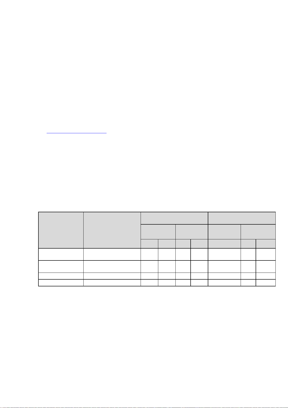
Optical modules
.
The optical power range depends on the particular SFP module that is fitted to the DAG
card. Optics modules are supplied in either Single or Multi mode. See the following table for
details.
Optical power is measured in dBm. This is decibels relative to 1 mW where 10 dB is
equivalent to a factor of 10 in power. A negative optical power value indicates power that is
less than 1 mW. The most sensitive devices can work at power levels down as low as -30dBm
or 1µW.
The DAG 3.8S card pluggable optics power module specification is shown below:
Product Number Network Support
Receive Characteristics Transmit Characteristics
Wavelength
(nm)
Sensitivity
(dBm)
Wavelength Tx Power
(dBm)
Min Max Min Max (nm) Min Max
TXR-OC3/OC12
MM
OC-3(STM-1) / OC-
12(STM-4) Multimode
1100 1600 -26 -14 1310 -20 -14
TXR-OC3/OC12 SM OC-3(STM-1) / OC-
12(STM-4) Single mode
1260 1600 -28 -8 1310 -15 -8
TRPD03MM3BAS OC-3 Multimode 1100 1600 -33 -12 1270 - 1380 -20 -14
TRPD12MM3EAS OC-12 Multimode 1100 1600 -28 -6 1270 - 1380 -20 -14
If there’s doubt check the card receiver ports light levels are correct using an optical power
meter.
Cover card transmit ports with LC-style plugs to prevent dust and mechanical hazards
damaging optics if not in use.

EDM01-09v15 DAG_3.8S_Card_User_Guide
©2005 - 2008 Endace Technology Ltd. Confidential - Version 14 - June 2008 11
Power Input
Note: The optical power input to the DAG card must be within the receiver’s dynamic
range. See the previous table for details. If it is slightly outside of this range it will
cause an increased bit error rate. If it is significantly outside of this range the system
will not be able to lock onto the signal.
When power is above the upper limit the optical receiver saturates and fails to function.
When power is below the lower limit the bit error rate increases until the device is unable to
obtain lock and fails. In extreme cases, excess power can damage the receiver.
When you set up the DAG card you should measure the optical power at the receiver and
ensure that it is within the specified power range. If it is not, adjust the input power as
follows:
•Insert an optical attenuator if power is too high, or
•Change the splitter ratio if power is too high or too low.
Splitter Losses
Splitters have the insertion losses either marked on their packaging or described in their
accompanying documentation. General guidelines are:
•A 50:50 splitter will have an insertion loss of between 3 dB and 4 dB on each output
•90:10 splitter will have losses of about 10 dB in the high loss output, and <2 dB in the
low loss output
Note: Endace recommends that you do not use a combination of single mode and multi
mode fibers and optics modules on the same link, as the quality of the received
signal cannot be guaranteed.
If you have no choice but to mix single mode and multi mode you should be aware
that a single mode input connected to a multi mode fiber will have some attenuation
but may still be acceptable. However a multi mode input connected to a single mode
fiber will likely have large and unpredictable losses.


EDM01-09v15 DAG_3.8S_Card_User_Guide
©2005 - 2008 Endace Technology Ltd. Confidential - Version 14 - June 2008 13
Configuring the DAG card
Introduction
Configuring the DAG 3.8S card ready for capturing data requires the following steps:
•Setting up the FPGA 14(page )
•Preparing the DAG card for use 17(page )
•Configuring the DAG Card 18(page )
•Viewing the DAG card statistics 29(page )
Once the DAG 3.8S is configured you can start capturing data, see Using your DAG card to
capture data 33(page ) for details on capturing data.
Before configuring the DAG card
Before configuring the FPGA, you should ensure that:
•dagmem has been run and memory allocated to each installed DAG card.
•dagload has been run so that all DAG drivers have been installed.
Refer to the Installing the drivers section for the required Operating system in EDM04-01 DAG
Software Installation Guide for the further details.
Firmware images
The following lists the features available on each firmware image available on this DAG card.
FPGA image
(Software version string)
OC3/12
STM1/4
ATM POS Co-
Processor
IPF
Co-
Processor
AAL5
TERF
dag38spci_erf.bit
(dag38spci_erf...)
dag38spci_terf.bit
(dag38spci_terf...)
dag38spci_cp1-aal5.bit
dag38spci_cp1-ipf.bit
dag38spp-erf.bit
The software version strings are displayed in the dagconfig output and when using the
dagrom -x command. They include a version number and creation date.

EDM01-09v15 DAG_3.8S_Card_User_Guide
14 ©2005 - 2008 Endace Technology Ltd. Confidential - Version 14 - June 2008
Setting up the FPGA
All DAG cards have at least one Field-Programmable Gate Array (FPGA). The FPGA
contains the firmware for the DAG card. The firmware defines how the DAG card operates
when capturing data and contains the specific configuration.
Note: Some DAG cards have multiple FPGA's.
For each FPGA there are two firmware images:
•a factory image - contains fixed basic functionality for operating the DAG card.
•a user image - contains an upgradable version of the DAG card firmware. Additional
functionality for the DAG card is available via the user image. Different user images
may be available with different functionality, i.e. TERF, DSM etc.
Firmware images are loaded into DAG card flash ROM in the factory. The image is
programmed into the FPGA each time the DAG card is powered up. The user image can
then be programmed into the FPGA either manually or via a script.

EDM01-09v15 DAG_3.8S_Card_User_Guide
©2005 - 2008 Endace Technology Ltd. Confidential - Version 14 - June 2008 15
Programming the FPGA
Before configuring the DAG card for capture, you must load and program the DAG card
with the appropriate FPGA image.
Note: For information about the dagrom options, see dagrom 16(page ).
To program the DAG 3.8S, type the following:
TERF
Load the PCI FPGA, type the following:
•dagrom -rvp -d0 -f dag38pci-terf.bit
Load the PHY FPGA image using: (Note: this loads this code into both PHY FPGA's)
•dagld -x -d0 dag38spp-erf.bit
ERF
Load the PCI FPGA, type the following:
•dagrom -rvp -d0 -f dag38spci-erf.bit
Load the PHY FPGA image using: (Note: this loads this code into both PHY FPGA's)
•dagld -x -d0 dag38spp-erf.bit
AAL5
Load the PCI FPGA, type the following:
•dagrom -rvp -d0 -f dag38spci_cp1-aal5.bit
Load the PHY FPGA image using: (Note: this loads this code into both PHY FPGA's)
•dagld -x -d0 dag38spp-erf.bit
Note: The Co-Processor needs to be programmed as well.
IPF
Load the PCI FPGA, type the following:
•dagrom -rvp -d0 -f dag38spci_cp1-ipf.bit
Load the PHY FPGA image using: (Note: this loads this code into both PHY FPGA's)
•dagld -x -d0 dag38spp_erf.bit
Note: The Co-Processor needs to be programmed as well.
(where "0" is the device number of the first DAG card). The filename of the FPGA image may
differ from the above depending on the version required.
Note: For information about the dagld options, see dagld (page 17).
If you get a message similar to the following in response to a dagconfig command check that
dagrom and dagld have been run correctly:
PP Xilinx not programmed!
If a Co-Processor is fitted on this DAG card, refer to EDM02-02 Co-Processor IP Filtering
Software Manual for details on how to program the Co-Processor.

EDM01-09v15 DAG_3.8S_Card_User_Guide
16 ©2005 - 2008 Endace Technology Ltd. Confidential - Version 14 - June 2008
dagrom
dagrom is a software utility that enables you to configure the FPGA on Endace DAG cards.
The following is a list of options available in dagrom.
Option Description
-a,--alternate-half
Use alternate (stable) half. [Default is current half.] Factory / User.
-A,--entire-rom
Entire ROM. [Default is current half only.]
-b,--swid-rom-check
Check if there is a SWID on the ROM.
-c,--cpu-region <region>
Access CPU region: c=copro, b=boot, k=kernel, f=filesystem.
--continue
Continue on erase error.
-d,--device <device>
DAG device to use.
-e,--erase
Erase ROM. [Default is read.]
-F,--disable-cfi-fast
Disable fast program option for CFI mode.
-f,--file <filename>
File to be read when programming ROM. There are multiple FGPA images
per DAG card, covering the different versions, ERF, TERF DSM etc.
--force
Force loading firmware. Dangerous.
-g,--rom-number <rom>
Access specified ROM controller. [Default is 0.]
-h,--help
-?,--usage
This page.
-i,--halt-ixp
Halt the embedded IXP Processor (DAG 7.1S only).
--image-table-fpga
<image table fpga>
Specify the Power On image selection table FPGA number
--image-table-image
<image table image>
Specify the Power On image selection table Image number
-j,--swid-rom-check-key
<key>
Check the ROM SWID key with the one supplied.
-l,--hold-bus
Hold PBI bus from XScale (DAG 3.7T only).
-m,--swid-key <key>
Hexadecimal key for writing the Software ID (aka SWID).
-o,--swid-rom-read
Read SWID from ROM.
-p,--program-current
Program current User 1 Xilinx image into FPGA.
-q,--image-number
<image number>
Specify the image number to write or to program the card.[0 - 3]. 0 factory
image, 1 user image 1, 2 user image 2, 3 user image 3. (7.5G2/G4 only)
--swid-write <swid>
Write given SWID. The key must be supplied with the -m option, requires a
valid running XScale ROM Image. (3.7T, 3.7D, 3.8S and 7.1S only)
-r,--reprogram
Reprogram ROM (may imply erase and write).
--reset-method
<reprogram method>
Specify the method to reprogram the card.[1.Ringo 2.George 3.Dave]
-s,--swid-rom-write
<swid>
Write given SWID to ROM. The key must be supplied with the -m option.
-t,--swid-read-bytes
<bytes>
Read <bytes> of SWID, requires a valid running XScale ROM image (3.7T
only)
-u,--swid-erase
Erase SWID from ROM.
--unknown
Force loading firmware. Dangerous.
-v,--verbose
Increase verbosity.
-V,--version
Display version information.
-w,--write
Write ROM (implies erase). [Default is read.]
--write-out <filename>
Write the contents of the ROM to a file.
-x,--list-revisions
Display Xilinx revision strings (the default if no arguments are given).
-y,--verify
Verify write to ROM.
-z,--zero
Zero ROM. [Default is read.]
All commands apply to the current image portion of the ROM, unless one of the options -a,
-A, -c is specified.
Note: Not all commands are supported by all DAG cards.
Other manuals for DAG 3.8S
1
Table of contents
Other Endace PCI Card manuals


Popular PCI Card manuals by other brands


 user guide")
Contec
Contec ADI12-16(PCI) user guide

CommTech
CommTech FASTCOM 422/4-PCI Hardware reference manual

Digital Equipment
Digital Equipment 9FX Vision 330 installation guide

Sigma
Sigma SQM-242 user guide

MEN Mikro Elektronik
MEN Mikro Elektronik F602 user manual

Fastcom
Fastcom 232/8-PCI Hardware reference manual