Enoch Systems JNC9B-F Operational manual

Product User Manual
and enterprise branch and head offices
JNC9B-F
-(7:$<
www.enochsystems.com 1-877-722-1116 [email protected]
Copyright © 2013 Enoch Systems, LLC, Enoch Systems and the Enoch Systems logo are trademarks or registered trademarks of Enoch Systems, LLC and/or its affiliates in the U.S. and other countries.
Third-party trademarks mentioned are the property of their respective owners. All rights reserved.

TECHNICAL MANUAL
Of
Intel HM67 Express Chipset
Based Mini-ITX M/B
No:G03-NC9B-F
Revision: 2.0
Release date: September 19, 2012
Trademark:
* Specifications and Information contained in this documentation are furnished for information use only, and are
subject to change at any time without notice, and should not be construed as a commitment by manufacturer.

i
Environmental Protection Announcement
Do not dispose this electronic device into the trash while discarding. To minimize
pollution and ensure environment protection of mother earth, please recycle.

ii
ENVIRONMENTAL SAFETY INSTRUCTION...........................................................................iii
USER’S NOTICE .......................................................................................................................iv
MANUAL REVISION INFORMATION.......................................................................................iv
ITEM CHECKLIST.....................................................................................................................iv
CHAPTER 1 INTRODUCTION OF THE MOTHERBOARD
1-1 FEATURE OF MOTHERBOARD................................................................................1
1-2 SPECIFICATION.........................................................................................................2
1-3 LAYOUT DIAGRAM....................................................................................................3
CHAPTER 2 HARDWARE INSTALLATION
2-1 JUMPER SETTING.....................................................................................................8
2-2 CONNECTORS AND HEADERS................................................................................11
2-2-1 CONNECTORS .............................................................................................11
2-2-2 HEADERS .....................................................................................................12
CHAPTER 3 INTRODUCING BIOS
3-1 ENTERING SETUP.....................................................................................................19
3-2 BIOS MENU SCREEN ................................................................................................20
3-3 FUNCTION KEYS .......................................................................................................20
3-4 GETTING HELP ..........................................................................................................21
3-5 MENU BAR..................................................................................................................21
3-6 MAIN MENU................................................................................................................22
3-7 ADVANCED MENU.....................................................................................................23
3-8 CHIPSET MENU..........................................................................................................29
3-9 BOOT MENU...............................................................................................................33
3-10 SECURITY MENU.......................................................................................................34
3-11 SAVE & EXIT MENU...................................................................................................35
TABLE OF CONTENT
iii
Environmental Safety Instruction
zAvoid the dusty, humidity and temperature extremes. Do not place the product in
any area where it may become wet.
z0 to 60 centigrade is the suitable temperature. (The figure comes from the request
of the main chipset)
zGenerally speaking, dramatic changes in temperature may lead to contact
malfunction and crackles due to constant thermal expansion and contraction from
the welding spots’ that connect components and PCB. Computer should go
through an adaptive phase before it boots when it is moved from a cold
environment to a warmer one to avoid condensation phenomenon. These water
drops attached on PCB or the surface of the components can bring about
phenomena as minor as computer instability resulted from corrosion and oxidation
from components and PCB or as major as short circuit that can burn the
components. Suggest starting the computer until the temperature goes up.
zThe increasing temperature of the capacitor may decrease the life of computer.
Using the close case may decrease the life of other device because the higher
temperature in the inner of the case.
zAttention to the heat sink when you over-clocking. The higher temperature may
decrease the life of the device and burned the capacitor.

iv
USER’S NOTICE
COPYRIGHT OF THIS MANUAL BELONGS TO THE MANUFACTURER. NO PART OF THIS MANUAL,
INCLUDING THE PRODUCTS AND SOFTWARE DESCRIBED IN IT MAY BE REPRODUCED, TRANSMITTED
OR TRANSLATED INTO ANY LANGUAGE IN ANY FORM OR BY ANY MEANS WITHOUT WRITTEN
PERMISSION OF THE MANUFACTURER.
THIS MANUAL CONTAINS ALL INFORMATION REQUIRED TO USE THIS MOTHER-BOARD SERIES AND WE
DO ASSURE THIS MANUAL MEETS USER’S REQUIREMENT BUT WILL CHANGE, CORRECT ANY TIME
WITHOUT NOTICE. MANUFACTURER PROVIDES THIS MANUAL “AS IS” WITHOUT WARRANTY OF ANY
KIND, AND WILL NOT BE LIABLE FOR ANY INDIRECT, SPECIAL, INCIDENTAL OR CONSEQUENTIAL
DAMAGES (INCLUDING DAMAGES FOR LOSS OF PROFIT, LOSS OF BUSINESS, LOSS OF USE OF DATA,
INTERRUPTION OF BUSINESS AND THE LIKE).
PRODUCTS AND CORPORATE NAMES APPEARING IN THIS MANUAL MAY OR MAY NOT BE
REGISTERED TRADEMARKS OR COPYRIGHTS OF THEIR RESPECTIVE COMPANIES, AND THEY ARE
USED ONLY FOR IDENTIFICATION OR EXPLANATION AND TO THE OWNER’S BENEFIT, WITHOUT
INTENT TO INFRINGE.
Manual Revision Information
Reversion Revision History Date
2.0 Second Edition September 19, 2012
Item Checklist
5Motherboard
5DVD for motherboard utilities
5Motherboard User’s Manual
5Cable(s)
5I/O Back panel shield

1
Chapter 1
Introduction of the Motherboard
1-1 Feature of Motherboard
zIntel HM67 express chipset
zIntel rPGA988B CPU socket supporting compatible Intel Core™ i3, i5, i7 Mobile
Processors
zSupport DDRIII DIMM 1066/1333 up to 16 GB and dual channel function
zOnboard Intel 82579 LM Gigabit Ethernet LAN
zIntegrated VIA VT 1705 6-channel HD Audio Codec
zSupport USB 2.0 data transport demands
zSupport USB 3.0 data transport demands
zSupport PCIE 2.0 by 16 Lane slot
zCompliance with ERP Standard.
zSupport Watchdog Timer Technology

2
1-2 Specification
Spec Description
Design zMini-ITX form factor 6 layers ; PCB size: 17.0x17.0cm
Chipset zIntel HM67 Express Chipset
CPU Socket zIntel socket G (rPGA 988B)
zSupport up to Intel Core™ i3, i5, i7 Mobile Processors
Memory Socket
z2 * SODIMMs Sockets
zSupport two DDRIII 1333/1066 MHz SODIMMs expandable
to 16 GB
zSupport dual channel function
Expansion Slot zPCIE 2.0 by 16 lane slot x1
zMini-PCIE slot x1
LAN Chip
zIntegrated Intel 82579LM Gigabit Ethernet LAN chip that
supports Fast Ethernet LAN function of providing
10Mb/100Mb/1000Mb Ethernet data transfer rate
zIntel 82579LM Gigabit Ethernet LAN chip supports Intel
Active Management Technology 7.0
Audio Chip zVIA VT 1705 6-channel HD Audio Codec integrated
zAudio driver and utility included
BIOS z32MB SMT Flash ROM
Multi I/O
zPS/2 keyboard connector x1
zHDMI connector x 1
zDVI connector x1 (HDMI Connector and DVI Connector can
not be used at the same time)
zVGA port connector x1
zUSB 2.0 port x4 and USB 2.0 header x2
zUSB 3.0 port x2
zE-SATA connector x1
zRJ-45 LAN connector x1
zAudio connector x1 (Line-in, Line-out, MIC)
zCoaxial S/PDIF Connector x1

3
zOptical S/PDIF Connector x1
zFront panel audio header x1
zSATAIII Connector x2
zSATAII Connector x3
zCDIN header x1
zLVDS header x1
zLVDS Inverter x1
zHDMI_SPDIF header x1
zSerial port header x1
zRS422/RS485 header x1
zFront panel header x1
zCIR header x1
zGPIO header x1
1-3 Layout Diagram
MIC-IN
VGA
Connector
Line-IN
Line-OUT
USB 3.0 Ports
PS/2 Keyboard
Connecter
HDMI
Connector
RJ-45 LAN Connector
DVI
Connector E-SATA
Connector
USB Ports
Coaxial
SPDIF OUT
Optical
SPDIF OUT

4
Audio Codec Chip
USB
Headers
PS/2 KB Port over
USB 3.0 Ports
JBAT1 SYS FAN2 Header
ATX Powe
r
Connector
ATX 12V Power
Connector
DDRIII Memory Modules
(DDRIII 1066/1333)
Front Panel
Header
S
p
eaker Header
CDIN1 Heade
r
DVI Connector
over VGA
Connector
Coaxical/Optical
SPDIF_OUT Connectors
E-SATA over
USB 2.0 Ports
Audio Connector
CI
R
Header
Intel
CPU Socket
HDMI Connector
RJ-45.over
USB 2.0 Ports
HDMI_SPDIF Header
Serial Port Heade
r
Front panel
Audio Header
Intel HM 67 Chi
p
se
t
SYS FAN1
Header
PCI Express 2.0 x16
by 16 lane slot
PWRLED1 Header
GPIO
Heade
r
CPUFAN
Header
LVDS Heade
r
LVDS Inverte
r
Gigabit PCI-E
LAN Chi
p
Mini-PCIE Slo
t
TX-RX COM
SATAII Ports
(SATA1/2/3/4/5)

5
JP1
JP3
JP5
JP6
JP7
JP8
JP9
JBAT 1
JP 4
6
Jumper
Jumper Name Description
JBAT1 CMOS RAM Clear Function Setting 3-pin Block
JP1 KB/MS Power On Function Setting 3-pin Block
JP3 LVDS PVCC 5V/3.3V Select 3-pin Block
JP4 USB Power On Function Setting 3-pin Block
JP5 Inverter power 5V/12V Select 3 pin Block
JP6 USB Power On Function Setting 3 pin Block
JP7 COM1 Header RS232/485/422 Function Select 6-pin Block
JP8 COM1 Header Pin9 function Select 6-pin Block
JP9 Mini PCI-E Slot Power 3.3V/3V Select 3-pin Block
Connectors
Connector Name Description
ATXPWR ATX Power Connector 24-pin Block
ATX12V ATX 12V Power Connector 4-pin Connector
KB(from UK1) PS2 Keyboard Connector 6-pin Female
HDMI High-Definition Multimedia Interface 19-pin Connector
VGA Video Graphic Attach Connector 15-pin Female
DVI Digital Visual Interface 24-pin Connector
USB (from
US1,UL1) USB Port Connectors 4-pin Connectors
USB (from UK1) USB Port Connectors 5-pin Connector
RJ-45 LAN
(from UL1) RJ-45 LAN Connectors 8-pin Connector
ESATA(from US1) External Serial ATAII Connector 7-pin Connector
SATA1/SATA2
SATA3/SATA4/
SATA5
Serial ATAII Connectors 7-pin Connectors
SPDIF_OUT Coaxial/Optical SPDIF out Connectors 2 -phone Jack
AUDIO1 Line Out /Line In /MIC Audio Connector 3 -phone Jack

7
Headers
Header Name Description
FP_AUDIO Front panel audio Headers 9-pin block
CDIN CD Audio-In Header 4-pin Block
INVERTER LVDS Inverter Connector 7-pin Block
LVDS LVDS Header 32-pin Block
HDMI-SPDIF SPDIF-Out header 2-pin Block
COM1 Serial Port Header 9-pin Block
TX-RXCOM RS 22/485 Port Header 4-pin block
USB1/USB2 USB 2.0 Port Headers 9- pin Block
PWR LED Power LED 3-pin Block
SPEAK Speaker Header 4-pin Block
CIR CIR Header 4-pin Block
JW_FP
(PWR LED/ HD LED/
/Power Button /Reset)
Front Panel Header
(PWR LED/ HD LED/ /Power
Button /Reset)
9-pin Block
CPUFAN,SYSFAN1/2 FAN Speed Headers 3-pin Block
GPIO_CON GPIO Header 10-pin Block
8
Chapter 2
Hardware Installation
2-1 Jumper Setting
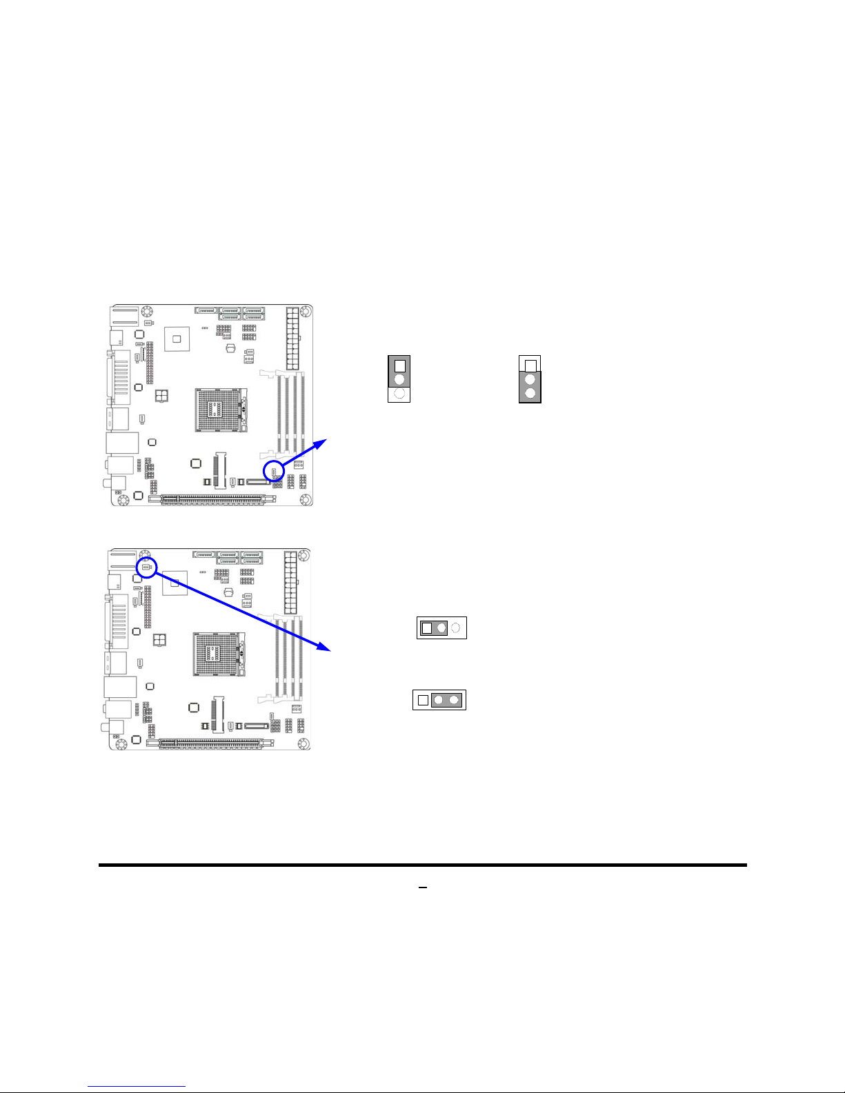
(1) Clear CMOS (3-pin): JBAT1
1 1 1
3 3
CMOS Clear Setting
2-3 Short:Clear CMOS
JBAT1
1-2 Short:Normal
(2) KB/MS Power On Function Setting (3-pin):JP1
2-3 closed: KB/MS Power-on Enabled
JP1
JP1
1-2 Closed: KB/MS Power-on Disabled(Default)
1
3
1
3
9
(3) LVDS PVCC 5V/3.3V Select (3-pin): JP3
2-3 closed: panel power3.3v
JP3
1-2 closed : panel power 5v
1
3
JP3 1
3
(4) USB Power On Function Setting (3-pin): JP4
2-3 closed: USB Power-on Enable
JP4
JP4
1-2 closed : USB Power-on Disable (Default)
1
3
1
3
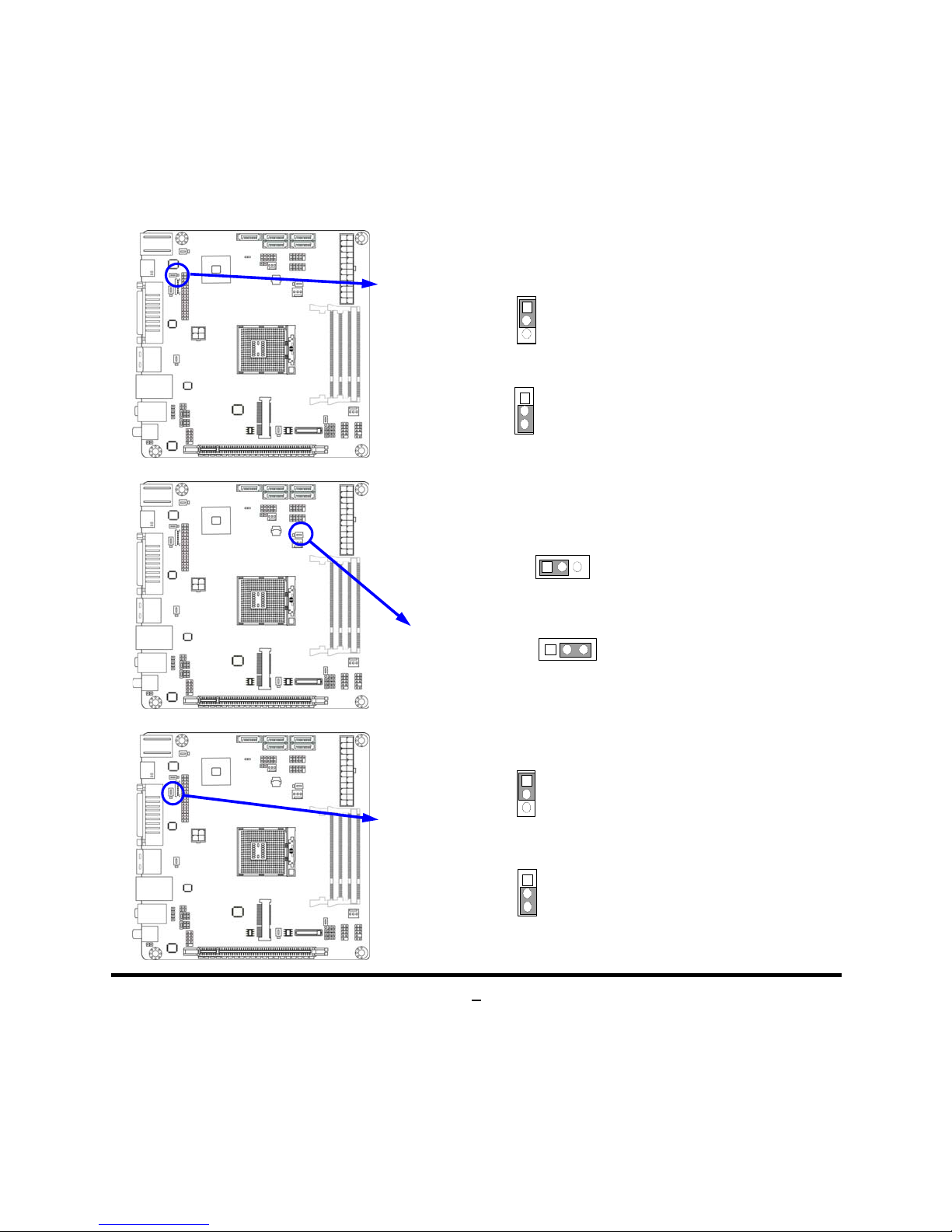
(5) Inverter power 5V/12V Select (3-pin):JP5
2-3 closed : Invertet power 12V
JP5
1-2 closed: Inverter power 5V
JP5
1
3
1
3

10
(6) USB Power On Function Setting (3-pin): JP6
1-2 closed: USB Power On Disable
2-3 closed: USB Power On Enable
JP6
JP6 1
3
1
3
(7) COM1 Header RS232/485/422 Function Select (6-pin): JP7
3-4 closed : RS485
JP7
1
1-2 closed: RS232
1
1
5-6 closed : RS422
(8) COM1 Header Pin9 function Select (6-pin): JP8
3-4 closed : +12V
JP8
1
1-2 closed: RS232
1
1
5-6 closed : +5V

11
(9) Mini PCI-E Slot Power 3.3V/3V Select (3-pin): JP9
2-3 closed :MINI PCI-E
Slot Power 3VSB
JP9
1-2 closed :MINI PCI-E
Slot Power 3.3V
JP9
1
3
1
3
2-2 Connectors and Headers
2-2-1 Connectors
(1) Rear Panel Connectors
(2) Serial-ATAII Port connector: SATA1/SATA2/SATA3/SATA4/SATA5
These connectors support the provided Serial ATA and Serial ATA2 hard disk cable to
connect the motherboard and serial ATA2 hard disk drives.
MIC-IN
VGA
Connector
Line-IN
Line-OUT
USB 3.0 Ports
PS/2 Keyboard
Connecter
HDMI
Connector
RJ-45 LAN Connector
DVI
Connector E-SATA
Connector
USB Ports
Coaxial
SPDIF OUT
Optical
SPDIF OUT

12
Serial-ATAII Connectors
SATA 3 SATA 5
SATA 4
SATA 2
SATA 1
2-2-2 Headers
(1) Line-Out, MIC-In Header (9-pin): FP_AUDIO
This header connects to Front Panel Line-out, MIC-In connector with cable.
Lin e-Out, MIC Headers
FP_AUDIO
Pin 1
MI
C
2-
L
LINEOUT2-L
MIC2-R
LINEOUUT2-R
NC
AUD
_
GN
D
NC
NC
AUD
_
JD
2
9
10

13
(2) CD AUDIO-In Headers (4-pin): CDIN
CDIN are the connectors for CD-Audio Input signal. Please connect it to CD-ROM
CD-Audio output connector.
CD Audio-In Headers
CDIN 4 1
GNDCD-R CD-LGND
(3) LVDS Inverter headers: INVERTER
Pin 1 and pin2: VCC of inverter
Pin3, pin4 and pin6: GND
Pin5: Backlight
Pin7: Brightness
Pin 1
VCC
VCC
GND
GND
Backlight
GND
Brightness

14
(4) LVDS Headers(32 Pin): LVDS
Pin NO. Pin Define Pin NO. Pin Define
Pin 1 LVDSB_DATAN3 Pin 2 LVDSB_DATAP3
Pin 3 LVDS_CLKBN Pin 4 LVDS_CLKBP
Pin 5 LVDSB_DATAN2 Pin 6 LVDSB_DATAP2
Pin 7 LVDSB_DATAN1 Pin 8 LVDSB_DATAP1
Pin 9 LVDSB_DATAN0 Pin 10 LVDSB_DATAP0
Pin 11 LVDS_DDC_DATA Pin 12 LVDS_DDC_CLK
Pin 13 GND Pin 14 GND
Pin 15 GND Pin 16 GND
Pin 17 LVDSA_DATAP3 Pin 18 LVDSA_DATAN3
Pin 19 LVDS_CLKAP Pin 20 LVDS_CLKAN
Pin 21 LVDSA_DATAP2 Pin 22 LVDSA_DATAN2
Pin 23 LVDSA_DATAP1 Pin 24 LVDSA_DATAN1
Pin 25 LVDSA_DATAP0 Pin 26 LVDSA_DATAN0
Pin 27 PVDD Pin 28 PVDD
Pin 29 PVDD Pin 30 PVDD
Pin 31 GND Pin 32 GND
Pin 1
LVDS Header
Pin 2
Table of contents
Other Enoch Systems Motherboard manuals


