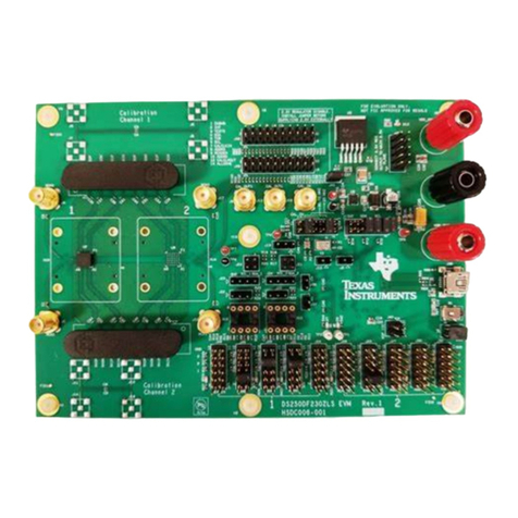
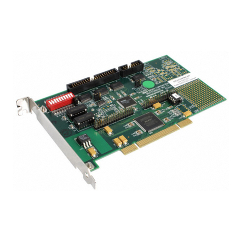
Texas Instruments TSW3000 User manual
Other Texas Instruments Motherboard manuals
Texas Instruments
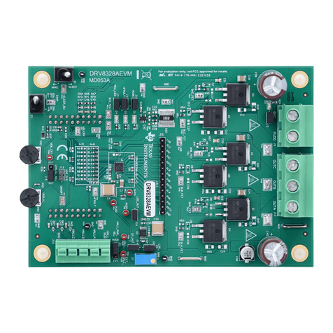
Texas Instruments DRV8328 EVM Series User manual
Texas Instruments
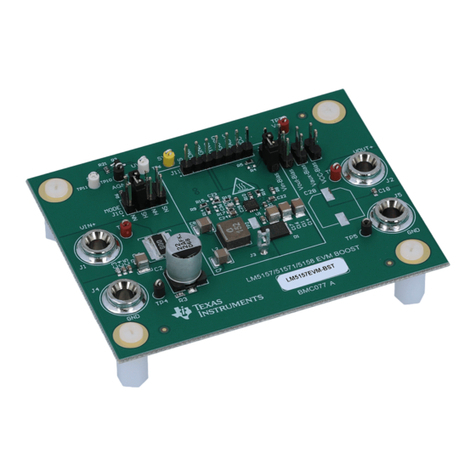
Texas Instruments LM5157EVM-BST User manual
Texas Instruments
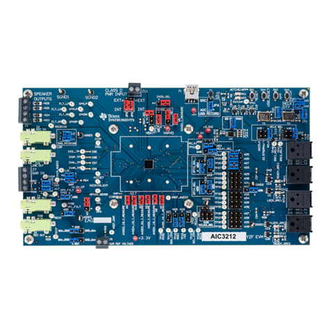
Texas Instruments TLV320AIC3212EVM-U User manual
Texas Instruments
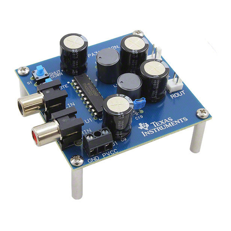
Texas Instruments TPA3125D2 EVM User manual
Texas Instruments
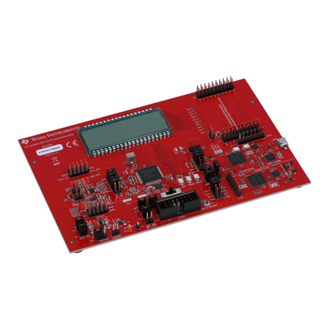
Texas Instruments EVM430-FR6043 User manual
Texas Instruments
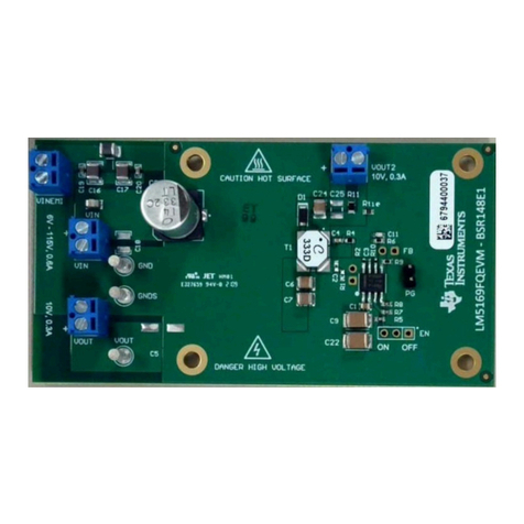
Texas Instruments LM5169FQEVM User manual
Texas Instruments
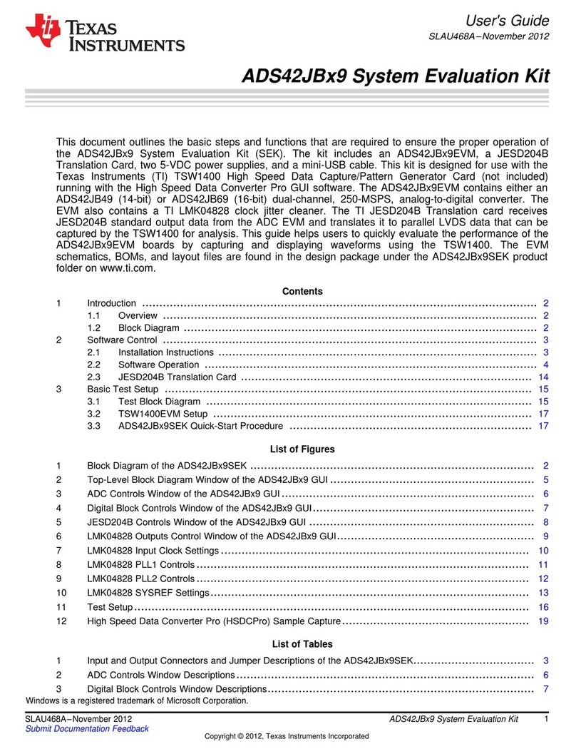
Texas Instruments ADS42JBx9 User manual
Texas Instruments
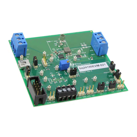
Texas Instruments bq24190 User manual
Texas Instruments
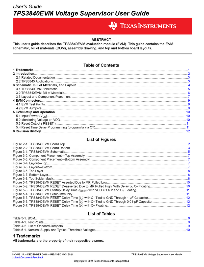
Texas Instruments TPS3840EVM User manual
Texas Instruments
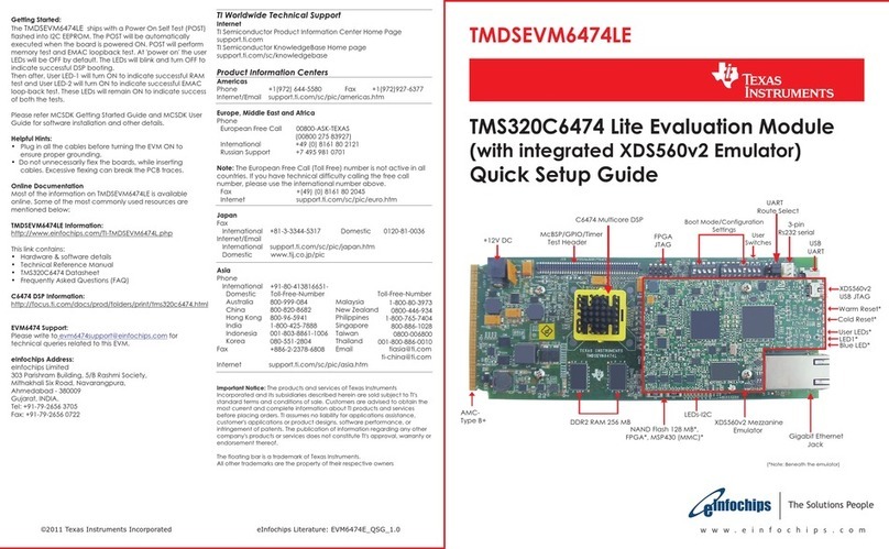
Texas Instruments TMDSEVM6474LE User manual
Texas Instruments
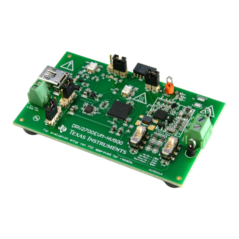
Texas Instruments DRV2700EVM-HV500 User manual

Texas Instruments
Texas Instruments SLVP125 EVM User manual
Texas Instruments
Texas Instruments DEM-DSD1796 User manual
Texas Instruments
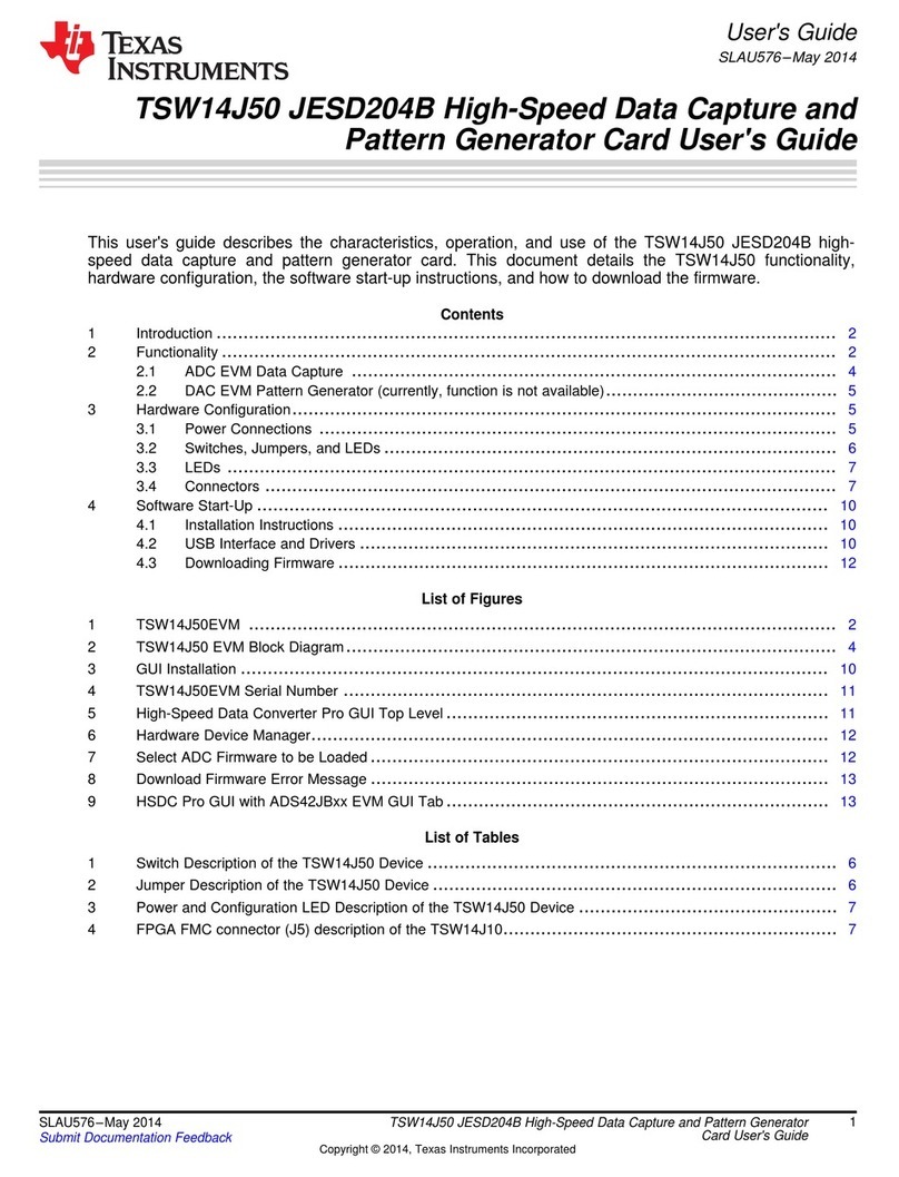
Texas Instruments TSW14J50 User manual
Texas Instruments
Texas Instruments TPS65980EVM User manual
Texas Instruments
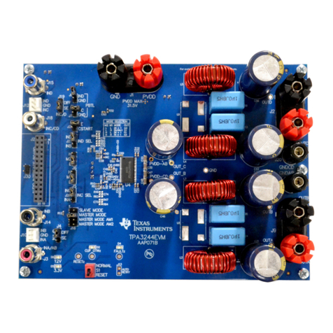
Texas Instruments TPA3244EVM User manual
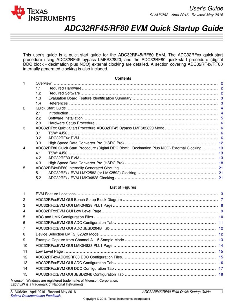
Texas Instruments
Texas Instruments ADC32RF45 EVM Troubleshooting guide

Texas Instruments
Texas Instruments ADS1625 EVM User manual
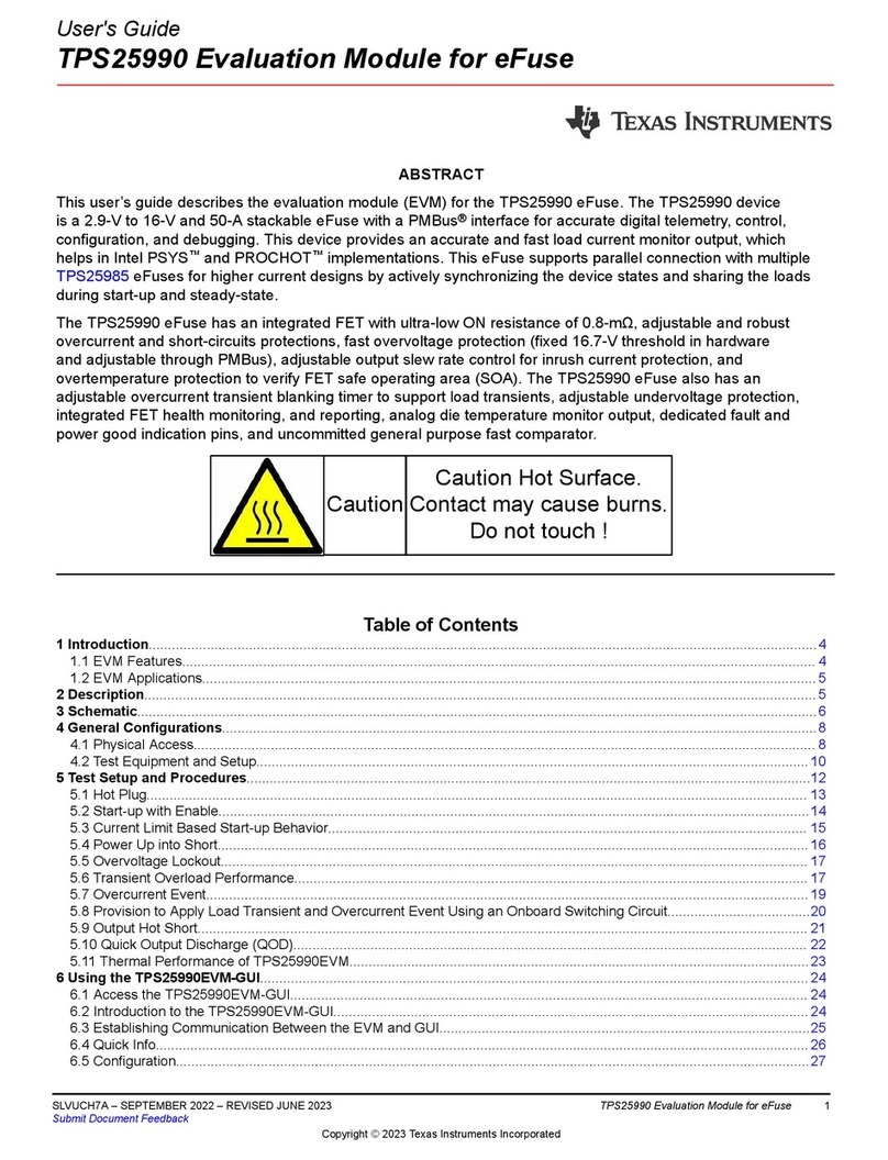
Texas Instruments
Texas Instruments TPS25990 User manual
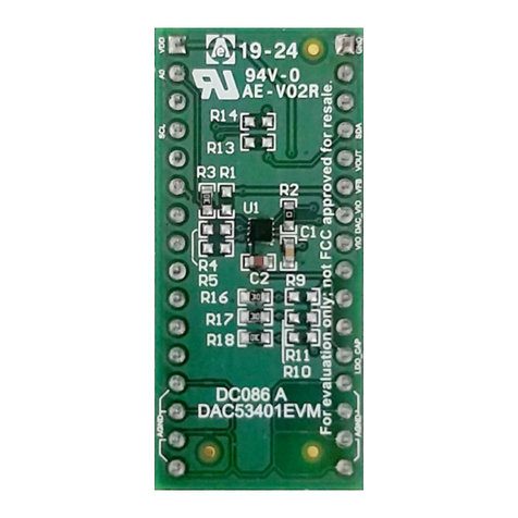
Texas Instruments
Texas Instruments DAC53401EVM User manual
