EPOX P55TV2 User manual

Introduction1-1
Chapter 1
Introduction
R
The P55TV2mainboard is a high performance system hardware based on
Intel Pentium processor and is equipped with four PCI slots, four standard
ISAslots, Ultra I/O controllerand dual port PCI-IDEconnectors for the
futureexpansion.Thehardwaredimensionis220mmx260mmwithafour-
layer-design technology.
Specification
Intel 82430VX PCIset chipset.
Intel Pentium Processor, Pentium Processor with MMX technology,
AMD K5/K6 and Cyrix M1/M2 operating at 90 ~ 266 MHz with 321 ZIF
socket 7 provides scalability to accept faster processors in the future.
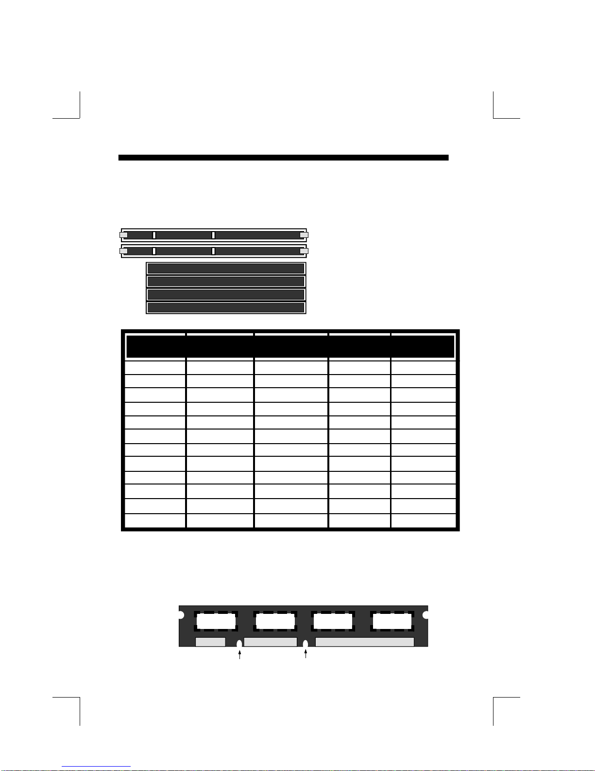
Supports up to 128 MegaBytes of DRAM (a minimum of 8 MB) on board
(72 Pins SIMM x 4, 168 Pins DIMM x 2). BIOS will autometically detect
and configure FP DRAM, EDO DRAM and SDRAM (Refer to Chapter 2-
3, System Memory Configuration).
Supports Onboard Pipelined Burst synchronous L2 Write Back Cache.
The cache memory combination can be 256KB/512KB (32KB*32 and
64KB*32 SRAM, respectively).
Supports four 16 bits ISA slots, four 32 bits PCI slots, and provides two
independent high performance PCI IDE interfaces capable of supporting
PIOMode3andMode 4 devices. TheP55TV2supportsfourPCIBus
Masters and a jumperless PCI INT# control scheme which reduces configu-
rationconfusionwhenpluggingin PCII/Ocontrollercard(s).
Supports AT API (e.g., CD-ROM) devices on both IDE interfaces.
Supports 1 floppy port, 1 parallel port (EPP,ECP port), 2 serial ports
(16550 Fast UART compatible) and 2 USB ports.
Supports a PS/2 style mouse and standard AT style keyboard connectors.
Supports Award Plug & Play BIOS. The BIOS is stored in Flash EPROM
form. It provides better upgradability for the system.
Supports CPU Hardware sleep and SMM (System Management Mode).
TheP55TV2utilizesaLithiumbatterywhichprovidesenvironmental
protection and longer battery life.
RTM
R

1-2 P55TV2
PCI#1
PCI#3
PCI#4
K/B
CONN.
PCI#2
Primary IDE
Secondary IDE
FDD CONN.
BANK0 BANK1
PowerConn.
82438
<
W83977
COM1
SIMM 1
SIMM 2
SIMM 3
SIMM 4
DIMM 2
DIMM 1
BIOS
USB Conn. COM2
82438VX
82438VX
64
K*32 64K*32
PRINTER
CN1
Socket 7
82437VX
Intel
Intel
82371SB
HD-LED TB-LED G-LED RESETSLEEP SPEAKER KEYLOCK J2
P55TV2 Layout
1
14
13
26
1 2
7 8
JP1
1
JP3
JP2
J1
1
Figure 1-1
J3
+12V
JP5
GND
GND
Note : Means Pin 1
JP6
2 1
8 7

Hardware Design 2-1
Chapter 2
Hardware design
2-1 Overview
TheP55TV2isdesignedwithIntel82430VX PCIset chipset whichisdevelopedby
INTELCorporationtofullysupportPentiumProcessorPCI/ISAsystem.TheIntel
82430VXPCIsetchipsetprovidesincreasedintegrationandimprovedperformance
designs.ThechipsetprovidesanintegratedIDEcontrollerwithtwohighperformance
IDEinterfacesforuptofourIDE devices (hard devices,CD-ROMdevice,etc).The
PnPUltraI/Ocontrollerprovidesthestandard PC I/O functions including:floppy
interface,two16ByteFIFOserialportsandoneEPP/ECPcapableparallelport.The
P55TV2layout is shown in the previous page for user's reference. Care must be
takenwheninsertingmemorymodules,insertingCPUorevenpluggingPCIcardinto
the associated slots to avoid damaging any circuits or sockets on board. A cooling
fanisstronglyrecommendedwheninstalling P54C/P54CTB/P55C/K5/K6/6x86/6x86L
processor due to possible overheat.
TheP55TV2supportsaminimumof8MBofSystemMemoryandamaximumof
128MB while L2 Cache can be 256KB/512KB synchronous SRAM Onboard to
increase system performance (Refer toPage 2-10 Cache Memory Configuration
for the details).
TheP55TV2supports standard Fast Page, EDO (Extended Data OutorHyperPage
Mode) or synchronous DRAM.The P55TV2provides four 72-pin SIMM and two
168-pinsDIMMsitesformemoryexpansion.Eachsocketsupports1Mx32(4MB),2M
x32(8MB),4Mx32(16MB),and8Mx32(32MB)single-sidedordouble-sidedmemory
modules.Thememorytimingrequires70nsFastpagedevicesor60nsEDODRAM.
Memoryparitygenerationandcheckingarenotsupported.(DRAMModulesmaybe
parity[x36]ornon-parity[x32].
TheP55TV2 supportsOnboardtwoPCIIDEconnectors,andBIOSdetectsIDE
harddisk type automatically.
The P55TV2supportsAwardPlug&Play BIOSforISAandPCI cards.TheBIOS is
located in Flash EPROM which is a technology to easily revise/upgrade BIOS
through software.
The P55TV2has been designed with Baby AT form-factor. The mainboard layout is
shown in Figure 1-1.
R

2-2 P55TV2
1
3
J3 The Power Supply (+12V) of the CPU Cooling FAN
1.GND
2.+12V
3.GND
1.Power LED(+)
2.N/C
3.GND
5.GND
4.Keylock
Sleep/Resume switch : Closed to enter sleep mode
(A keystrobe or mouse movement will instantly "wake up".)
Power Saving LED indicator - LED ON when system is in any
saving mode
Turbo LED indicator - LED ON when higher speed is selected
Harddisk LED indicator - LED ON when Onboard PCI IDE
Harddisks activites
2-2 Connectors and Jumpers
This section describes all of the connectors and jumpers built into the mainboard.
Please refer to Figure 1-1 (page 1-2) for the location of each connector and
jumper. The following figures shows connector and jumper setting. means
connecting to pins 1&2 and means connecting to pins 2&3.
means setting jumpers with two pins open, and means setting
jumpers with two pins close.
J2 KeyLock - Keyboard lock switch & Power LED connector.
Speaker - connect to the system's speaker for beeping
7. Speaker
8. N/C
9. GND
10. VCC
Reset - Closed to restart system
1
5
+
+
+

Hardware Design 2-3
1 . Data (Red Wire)
2 . Clock (Blue Wire)
3 . GND (Green)
5 . VCC (Yellow)
4 . NC
1J1 PS/2 MOUSE CONNECTOR
5
1 . VCC
2 . NC
3 . IRRX
5 . IRTX
4 . GND
1J4 IrDA/ASK IR CONNECTOR
5
12
1615
CN1 USB CONNECTOR
Reserved for USB port Adapter
(refer to APPENDIX B:I/O Connectors)
JP3 BIOS Flash Mode Selection
1-2 : Normal operation (Default)
2-3 : BootBlock Flash
3
1
JP1 DIMM Working Voltage Selection
1-2, 3-4 : 5V
5-6, 7-8 : 3.3V (Default)
(Refer to 2-4 : Memory Configuration for the detail)
1 2
7 8
JP2 EPROM BIOS Selection
1-2 : 5V Flash ROM (Default)
2-3 : 12V Flash ROM
3
1

2-4 P55TV2
JP6 : CPU Vcore voltage selection : For Pentium MMX Processor, AMD K6
and Cyrix 6x86L/MX
1-2 : 2.8V for Pentium MMX Processor and Cyrix 6x86L
3-4 : 2.9V for AMD K6-PR2-166/200 and Cyrix 6x86MX
5-6 : 3.2V for AMD K6-PR2-233/266
7-8 : 3.5V for Pentium, AMD K5 and Cyrix 6x86
7 8
1 2
JP5 : CPU Clock Rate Selection (Single Jumper)
These jumper settings are reserved for the future
CPU versions. when the future CPUversions are
ready and suitable for this mainboard, these jumper
settings will be correctly updated.
*
13 26
Pentium BusFreqency
PentiumMMX x Cyrix 6x86(L) / 6x86MX
AMDK5/ K6 Multiplier IBM 6x86(L)/6x86MX
JP5
1 14
CPU
1-14 90MHz 60MHz x 1.5
2-15 100MHz 66MHz x 1.5
3-16 120MHz 60MHz x 2 6x86/L-PR150
4-17 133MHz 66MHz x 2 6x86/L/MX-PR166
5-18 150MHz 60MHz x 2.5 6x86MX-PR166
6-19 166MHz 66MHz x 2.5 6x86MX-PR200
7-20 188MHz 75MHz x 2.5 6x86MX-PR233
8-21 200MHz 66MHz x 3 6x86MX-PR233
9-22 225MHz 75MHz x 3 6x86MX-PR266
10-23 233MHz 66MHz x 3.5 6x86MX-PR266
11-24 266MHz 66MHz x 4
12-25 110MHz 55MHz x 2 6x86/L-PR133
13-26 150MHz 75MHz x 2 6x86/L/MX-PR200
*
*
*
*
*

Hardware Design 2-5
2-3
Real Time Clock Battery Replacement
Thebatterycan bereplacedwithanequivalentcoinlithiumbattery
suchasSanyo/PanasonicCR2032.Pleasefollowthefollowing stepsto
replacethebattery.
+
+
+
+
+
+
+
1.Remove 2.Insert
1
2
3
4
1
2
3

2-6 P55TV2
2-4SystemMemoryConfiguration
The P55TV2 supports different types of settings for the system memory. The
memoryconfigurationdoesnotneedjumperor hardware setting. Thefollowing
tablesprovide all possible memory combinations.
Installed
Installed
None
None
None
None
Installed
None
Installed
None
Installed
Installed
Installed
None
None
Installed
None
Installed
Installed
Installed
None
None
None
None
Installed
(BANK 0) (BANK 1) (BANK 0) (BANK1)
OK
OK
OK
OK
OK
OK
OK
OK
Notallowed
Notallowed
Installed Installed
Notallowed
Notallowed
SIMM3,4 SIMM1,2 DIMM2 DIMM1 STATUS
None
None
Installed
None
None
Installed
Installed
Installed
None
None
None
Installed
Installed
None
None
Installed
Installed
None
Installed
None
None
>
>
SIMM4
SIMM2
SIMM3
SIMM1
BANK 0 5V FP / EDO DRAM
BANK 1 5V FP / EDO DRAM
DIMM1 >
BANK 1
DIMM2 BANK 0
>Synchronous DRAM
or FP / EDO DRAM
Synchronous DRAM
or FP / EDO DRAM
LEFT KEY ZONE CENTER KEY ZONE
(3.3 V DRAM)
(UNBUFFERED)
NOTE: 1.The P55TV2 supports both Fast PageDRAMandEDODRAMSIMMs,but
they cannot be used in the same memory bank.
2.The KEY ZOOM of the DIMM socket is 3.3V/Unbuffered
DRAM chip

Hardware Design 2-7
Memory Configuration Table1
TOTAL
4M x 2 (8 MB)
4M x 2 (8 MB)
8M x 2 (16 MB)
8M x 2 (16 MB)
16M x 2 (32 MB)
16M x 2 (32 MB)
32M x 2 (64 MB)
Empty
Empty
Empty
Empty
Empty
Empty
Empty
Empty
Empty
Empty
Empty
Empty
Empty
Empty
Empty
Empty
Empty
Empty
Empty
Empty
Empty
Empty
Empty
Empty
Empty
Empty
Empty
Empty
Empty
Empty
Empty
Empty
4M x 2 (8 MB)
4M x 2 (8 MB)
4M x 2 (8 MB)
8M x 2 (16 MB)
8M x 2 (16 MB)
8M x 2 (16 MB)
16M x 2 (32 MB)
16M x 2 (32 MB)
16M x 2 (32 MB)
32M x 2 (64 MB)
32M x 2 (64 MB)
32M x 2 (64 MB)
SIMM1,2(Bank1)
4M x 2 (8 MB)
8M x 2 (16 MB)
Empty
16M x 2 (32 MB)
16M x 2 (32 MB)
4M x 2 (8 MB)
16M x 2 (32 MB)
16M x 2 (32 MB)
8M x 2 (16 MB)
32M x 2 (64 MB)
32M x 2 (64 MB)
DIMM2(Bank0) DIMM1(Bank1)SIMM3,4(Bank0) 8MB
16MB
40MB
72MB
16MB
24MB
48MB
80MB
32MB
40MB
48MB
64MB
96MB
72MB
64MB
80MB
96MB
128MB
24MB
32MB
Empty
EmptyEmpty
Empty
Empty
Empty
4M x 2 (8 MB)
Empty
32M x 2 (64 MB)
8M x 2 (16 MB)
32M x 2 (64 MB) 32M x 2 (64 MB)
4M x 2 (8 MB)
Empty
8M x 2 (16 MB)
Empty
Empty
Empty
The P55TV2 supports two 168-pin DIMM module sockets to extpand system
memory size.You can install (3.3V/Unbuffered) Fast Page, EDO or
Synchronous DRAM. Besides, to support 5V FP and EDO DRAM with DIMM
socket, the P55TV2 provides JP1 to allow user using 3.3V/Unbuffered DIMM
module with 5V FP and EDO DRAM chips. The setting of the JP1 as follow:
When you plug a DIMM module into a 168-pin dual readout socket, you must
make sure that the key zoom of the DIMM module is 3.3V/Unbuffered and
supports Intel Pentium Processor System.
R
7 8
JP1 DIMM Working Voltage Selection
1-2, 3-4 : For 5V FP and EDO DRAM
5-6, 7-8 : For 3.3V FP, EDO and Synchronous DRAM
1 2

2-8 P55TV2
8MB
8MB
8MB
8MB
8MB
16MB
16MB
16MB
16MB
16MB
32MB
32MB
32MB
32MB
32MB
64MB
64MB
64MB
64MB
64MB
Empty
Empty
Empty
Empty
Empty
Empty
Empty
Empty
Empty
Empty
Empty
Empty
Empty
Empty
Empty
Empty
Empty
Empty
SIMM3,4(Bank0) DIMM2(Bank0)
SIMM1,2(Bank1)
Memory Configuration Table2
Empty
Empty
Empty
Empty
Empty
Empty
Empty
4M x 2 (8 MB)
8M x 2 (16 MB)
Empty 16M x 2 (32 MB)
4M x 2 (8 MB)
8M x 2 (16 MB)
16M x 2 (32 MB)
8MB
8MB
8MB
8MB
16MB
16MB
16MB
16MB
16MB
Empty
Empty Empty
Empty
Empty
Empty
Empty
Empty
Empty
Empty
Empty
Empty
SIMM1,2(Bank1)
Memory Configuration Table3
DIMM1(Bank1)
DIMM2(Bank0)
TOTAL
16MB
48MB
40MB
8MB
16MB
24MB
40MB
72MB
24MB
80MB
32MB
48MB
64MB
96MB
72MB
64MB
96MB
128MB
32MB
80MB
TOTAL
8MB
16MB
24MB
40MB
72MB
16MB
24MB
32MB
48MB
80MB
Table 3(CONT.)
32M x 2 (64 MB)Empty
Empty
32M x 2 (64 MB) 8MB
Empty
Empty
Empty
Empty
Empty
Empty
Empty
Empty
Empty
Empty
Empty
Empty
Empty
Empty
Empty
Empty
Empty
Empty
Empty
Empty Empty
8MB
16MB
32MB
64MB
Empty
8MB
16MB
32MB
64MB
Empty
8MB
16MB
32MB
64MB
Empty
8MB
16MB
32MB
64MBEmpty
Empty
SIMM3,4(Bank0) DIMM1(Bank1)

Hardware Design 2-9
SIMM1,2(Bank1) DIMM1(Bank1)
SIMM3,4(Bank0)
32M x 2 (64 MB)
4M x 2 (8 MB)
8M x 2 (16 MB)
16M x 2 (32 MB)
32MB
32MB
32MB
32MB
32MB
64MB
64MB
64MB
64MB
64MB
Empty
Empty
Empty
Empty
Empty
Empty
Empty
Empty
Empty
Empty
Empty Empty
Empty
Empty
Memory Configuration Table3 (CONT.)
DIMM2(Bank0)
Empty
Empty
Empty
Empty
Empty
Empty
Empty
Empty
Empty
Empty
Empty
Empty
Empty
Empty
Empty
Empty
Empty
Empty
Empty
4M x 2 (8 MB)
8M x 2 (16 MB)
32M x 2 (64 MB)
16M x 2 (32 MB)
8M x 2 (16 MB)
32M x 2 (64 MB)
16M x 2 (32 MB)
4M x 2 (8 MB)
8M x 2 (16 MB)
16M x 2 (32 MB)
4M x 2 (8 MB)
8M x 2 (16 MB)
16M x 2 (32 MB)
Empty
Empty
Empty
Empty 8MB
8MB
8MB
8MB
8MB
16MB
16MB
16MB
16MB
16MB
32MB
32MB
32MB
32MB
32MB
64MB
64MB
64MB
64MB
Empty
Empty
Empty
Empty
Empty
Empty
Empty
Empty
Empty
Empty
Empty
Empty
Empty
Empty
Empty
Empty
Empty
Empty
Empty
SIMM1,2(Bank1)SIMM3,4(Bank0) DIMM2(Bank0) DIMM1(Bank1)
Memory Configuration Table4
TOTAL
32MB
40MB
48MB
64MB
96MB
72MB
64MB
80MB
96MB
128MB
8MB
16MB
24MB
40MB
72MB
16MB
24MB
32MB
48MB
80MB
32MB
40MB
48MB
64MB
96MB
72MB
64MB
80MB
96MB
TOTAL
Empty 64MB 128MBEmpty
32M x 2 (64 MB)
32M x 2 (64 MB)
4M x 2 (8 MB)
32M x 2 (64 MB)
16M x 2 (32 MB)
8M x 2 (16 MB)
4M x 2 (8 MB)
Empty
Empty
Empty
Empty
Empty
Empty
Empty
Empty

2-10 P55TV2
SIMM1,2(Bank1)SIMM3,4(Bank0)
8MB
32MB
8MB
8MB
32MB
4M x 2 (8 MB) 8MB
4M x 2 (8 MB)
16M x 2 (32 MB)
4M x 2 (8 MB)
16M x 2 (32 MB)
16M x 2 (32 MB)
4M x 2 (8 MB)
4M x 2 (8 MB)
4M x 2 (8 MB)
16M x 2 (32 MB)
16M x 2 (32 MB)
16M x 2 (32 MB)
8MB
32MB
32MB
8MB
32MB
32MB
Memory Configuration Table5
DIMM2(Bank0) DIMM1(Bank1) TOTAL
32MB
56MB
72MB
80MB
104MB
128MB
1, Assume all DRAM and SDRAM in Table 5 are single-side.
2,TheP55TV2Supportsandextendsmanymemoryconfigurationsonits4SIMM and
2DIMMsites. The memory size of any configuration canbecombinedflexibly.
The above tables only list the basic memory configurations for your reference.
Many configurations are not listed, you may use other configurations not listed
on the above. BIOS will detect your memory configuration automatically.
2-5CacheMemoryConfiguration
The second level (L2) cache is installed in the mainboard to increase the system
performance. The P55TV2supports512KBcache(piplinedburstSRAM).
64K*32
64K*32
U22
16K*8
TAG SRAM
U16 U21
DATA SRAM
Note :
3, The 70ns Fast Page Mode or 60ns EDO DRAM is necessary.
Usually,theDIMM2andSIMM3&4occupythesamememoryblock,Bank0.They
cannotbeinstalledatthesametime.Likewise,theDIMM1andSIMM1&2occupy
thesamememoryblock,Bank1.Theycannotbeinstalledatthesametimeeither.
Howeverwithaspecialdesigntoexpandmemory,theP55TV2allowsyouto
upgradesingle-sideDRAMatDIMM2(Bank0)andDIMM1(Bank1),ifyouuse
single-sideDRAMattheSIMM3&4andSIMM1&2.
Regardingsingle-sideordouble-sideDRAM/SDRAM,pleasecontactyourDRAM/
SDRAMsuppliersforthedetails,
4,

Hardware Design 2-11
2-6IntegratedPCIBridge
The P55TV2utilizes Intel's430VXPCIsetchipsettosupportIntelPentium Proces-
sorPCI/ISA system.TheIntel82430VXPCIsetchipsetconsistsofone82437VX
systemcontroller(TVC),two82438VXDataPath(TDP)devices,andone82371SB
PCIISA/IDEAccelerator(PIIX3)bridgechip.Itprovidesaninterfacewhichtrans-
latesCPUcycleintoPCIbuscycleandPCI burst read/write capability. In addition, it
provideshighperformance PCI arbiter or supports four PCI Masters,Rotating
PriorityMechanism,andHiddenArbitrationSchemeMinimizesArbitrationOver-
head.The82371SB(PIIX3)supportsPCISpecificationRevision2.1Compliantand
contains a Universal Serial Bus interface with both host and hub control functions.
TheP55TV2 reserves USB connector toprovidetwoUSB ports for serial transferat
12 or 1.5 Mbit/sec. This will supports legacy keyboard and mouse software with
USB-Base Keyboard and mouse.
TherearefourinterruptsineachPCIslot:INTA#,INTB#,INTC#,andINTD#,since
the P55TV2adapts the PCI auto-configuration with the system BIOS Setup utility.
Whenthesystemis turned on after adding a PCI add-incard,theBIOSautomatically
configure interrupts, DMA channels, I/O space, and other paramaters. You do not
have to configure jumpers or worry about potential resource conflicts. Because PCI
cards use the same interrupt resource as ISA cards, you must specify the interrupts
used by ISA add-in cards in the BIOS Setup utility.
If a "Legacy card" (such as paddle card and cable) is plugged into the ISA slot the
following modifications in the ROM SETUP UTILITY become necessary. First,
enter PCI CONFIGURATION SETUPutility from ROM SETUP UTILITY
main menu to set the "PCI IDE IRQ MAP TO : ISA".
Second, enter CHIPSET FEATURES SETUP UTILITYfrom ROM SETUP
UTILITY main menu and set the "Onboard Primary PCI IDE: Disabled and
Onboard Secondary PCI IDE: Disabled." When you plugg the PCI/ISA IDE card
into the system, You shouldDisabled Onboard Primary and Secondary PCI IDE
from CHIPSET FEATURES SETUP UTILITYtoo.
you can set the system interrupt request (IRQ) on some "Legacy cardswhich have
no paddle card and cable" (refer to user's manual of the card) to a proper system
IRQ level (In general, the card's Primary is assigned to INTA and Secondary is
assigned to INTB). If the card is plugged into slot 1(marked PCI#1), you cannot
use second slot (marked PCI#2) because the Secondary INT signal takes INTB
from the slot (Refer to Page 3-12 for circuit diagram). The user then enters PCI
CONFIGURATION SETUPutility from ROM SETUP UTILITY main menu
and sets the "PCI IDE IRQ MAP TO : PCI-Slot 1" (depend on the slot # where
the Legacy card is plugged).
.
R

AWARD BIOS 3-1
ROM PCI/ISA BIOS(2A59GPAC)
CMOSSETUPUTILITY
AWARDSOFTWARE,INC.
STANDARD CMOS SETUP SUPERVISOR PASSWORD
BIOS FEATURES SETUP USER PASSWORD
CHIPSET FEATURES SETUP IDE HDD AUTO DETECTION
POWER MANAGEMENT SETUP HDD LOW LEVEL FORMAT
PNP/PCI CONFIGURATION SAVE & EXIT SETUP
INTEGRATED PERIPHERALS EXIT WITHOUT SAVING
LOAD SETUP DEFAULTS
ESC : QUIT : SELECT ITEM
F10 : Save & Exit Setup (Shift)F2 : Change Color
Time, Date, Hard Disk Type...
Figure 3-1 CMOS SETUP UTILITY
The menu displays all the major selection items. Select the item you need to
reconfigure. The selection is made by moving cursor (press any direction key ) to the
item and press the 'Enter' key. An on-line help message is displayed at the bottom of
the screen as the cursor is moving to various items which provides a better under-
standing of each function. When a selection is made, the menu of selected item will
appear so the user can modify associated configuration parameters.
Chapter 3
AWARD BIOS Setup
Award'sROMBIOSprovidesabuilt-inSetupprogramwhichallowsusertomodifythe
basicsystemconfigurationandhardwareparameters.Themodifieddatawillbestored
inabattery-backedCMOSRAMsodatawillberetainedevenwhenthepoweristurned
off. In general, the information saved in the CMOS RAM stay unchanged unless there
isaconfigurationchangeinthesystem,suchasaharddrivereplacementoranewdevice
installment.
It is possible for the CMOS battery to fail. This will cause data lose in CMOS only.If
this does happen you will need to reconfigure your configuration parameters.
To enter Setup Propgram
Poweronthecomputerandpress<Del>keyimmediately.ThiswillbringyouintoBIOS
CMOSSETUPUTILITY.

3-2 CHAPTER 3
3-1STANDARDCMOSSETUP
Choose"STANDARDCMOSSETUP"intheCMOSSETUPUTILITYMenu(Fig.3-
1).The STANDARDCMOSSETUPallowsusertoconfiguresystemsetting suchas the
currentdateandtime,typeofharddiskdriveinstalled, floppydrivetype,anddisplaytype.
Memorysizeisauto-detectedbytheBIOSanddisplayedforyourreference.Whenafield
ishighlighted(usedirectionkeystomovecursorand<Enter>keytoselect),theentryin
thefieldwillbechangedbypressing<PgDn>or<PgUp>keysorusercanenternewdata
directlyfrom the keyboard.
Figure 3-2 STANDARD CMOS SETUP
Selectingthe"BIOSFEATURESSETUP"optionintheCMOSSETUPUTILITYmenu
allowsusertochangesystemrelatedparametersinthedisplayedmenu.Thismenushows
allofthemanufacturer's defaultvaluesoftheP55TV2.Again, usercanmovethecursor
by pressing direction keys and <PgDn> or <PgUp> keys to modify the parameters.
Pressing [F1] key to display help message of the selected item.
This setup program also provides 2 convenient ways to load the default parameter data
fromBIOS[F6]orCMOS[F7]areaif theshowndataiscorrupted.Thisprovides thesystem
a capability to recover from any possible error.
3-2BIOSFEATURESSETUP
NOTE: The "Halt On :" field is to determine when to halt the system by the BIOS if an error
occurrs.
NOTE: If hard disk Primary Master/Slave and Secondary Master/Slave use Auto,
then the hard disk size and model will be auto-detected.
ROMPCI/ISABIOS(2A59GPAC)
STANDARDCMOSSETUP
AWARDSOFTWARE,INC.
ESC : Quit : Select Item PU/PD/+/- : Modify
F1 : Help (Shift) F2 : Change Color
Date (mm:dd:yy) : Wed, Apr 17 1996
Time (hh:mm:ss) : 14 : 30 : 50
HARD DISKS TYPE SIZE CYLS HEAD PRECOMP LANDZONE SECTORS MODE
Primary Master : Auto 0 00 0 0 0 Auto
Primary Slave : Auto 0 00 0 0 0 Auto
Secondary Master :Auto 0 00 0 0 0 Auto
Secondary Slave :Auto 0 00 0 0 0 Auto
Drive A : 1.44M, 3.5 in.
Drive B : None
Floppy 3 Mode Support : Disabled
Video : EGA/VGA
Halt On : All Errors
Base Memory :640K
Extended Memory :31744K
Other Memory :384K
Total Memory :32768K

AWARD BIOS 3-3
Note: The Security Option contians "setup" and "system". The "setup" indicates
that the password setting is for CMOS only while the "system" indicates the
password setting is for both CMOS and system boot up.
CPUInternalCache/ExternalCache: Thesetwocategoriesspeedupmemory
access. However, it depends on CPU/chipset design. The default value is Enabled.
IfyourCPUiswithout InternalCachethentheitem"CPUInternal Cache"willnot
show.
Enabled:Enable cache.
Disable : Disable cache.
Virus Warning: This category flashes on the screen. During and after the system
boots up, any attempts to write to the boot sector or partition table of the hard disk
drive will halt the system and an error message will appear. You should then run an
anti-virus program to locate the virus. Keep in mind that this feature protects only the
boot sector, not the entire hard drive. Default value is Disabled
Enabled : Activate automatically when the system boots up causing a warning
message to appear when any attempts to access the boot sector or the
harddiskpartitiontable.
Disabled:No warning message to appear when any attempts to access the boot
sector or the hard disk partition table.
ROMPCI/ISABIOS(2A59GPAC)
BIOSFEATURESSETUP
AWARDSOFTWARE,INC.
Esc : Quit : Select Item
F1 : Help PU/PD/+/- : Modify
F5 : Old Values (Shift)F2 : Color
F7 : Load Setup Defaults
Figure 3-3 BIOS FEATURES SETUP
Virus Warning :Disabled Video BIOS Shadow :Enabled
CPU Internal Cache :Enabled C8000-CBFFF Shadow :Disabled
External Cache :Enabled CC000-CFFFF Shadow :Disabled
Quick Power On Self Test :Enabled D0000-D3FFF Shadow :Disabled
Boot Sequence :A,C, SCSI D4000-D7FFF Shadow :Disabled
Swap Floppy Drive :Disabled D8000-DBFFF Shadow :Disabled
Boot Up Floppy Seek :Enabled DC000-DFFFF Shadow :Disabled
Boot Up NumLock Status :On
Boot UP System Speed :High
Gate A20 option :Fast
Typematic Rate Setting : Disabled
Typematic Rate (Chars/Sec) : 6
Type matic Delay (Msec) : 250
Security Option : Setup
PCI/VGA Palette Snoop : Disabled
OS Select For DRAM > 64MB : Non-OS2

3-4 CHAPTER 3
Quick Power On Self Test:This category speeds up Power On Self Test (POST)
after you power on the computer. If it is set to Enable, BIOS will shorten or skip
some check items during POST.
Enabled : Enable quick POST.
Disabled: Normal POST.
BootSequence:Thiscategorydetermines which drive issearchedfor first for
theO/S(OperatingSystem).DefaultvalueisA,C.
A,C : System will first search for the floppy disk drive then the hard disk drive.
C,A : System will first search for the hard disk drive then the floppy disk drive.
CDROM,C,A: SystemwillfirstsearchfortheCDROMdrive(IftheCDROMhasa
bootable CD title.) and second search for the hard disk drive then the
flopp disk drive.
C,CDROM,A: Systemwillfirstsearchforthe hard diskdriverandsecondsearchfor
the CDROM drive (If the CDROM has a bootable CD title.) then the
floppy disk drive.
SwapFloppy Drive:ThiswillswapyourphysicaldrivelettersA&Bifyouareusing
two floppy disks. Default value is Disabled.
Enabled : Floppy A & B will be swapped under the O/S.
Disabled:Floppy A & B will be not swapped.
Boot Up NumLock Status:The default value is On.
On : Keypad is number keys.
Off : Keypad is arrow keys.
BootUP System Speed: Select the default system speed. The system will run at the
selected speed after the system boots.
High: Set the speed to high.
Low : Set the speed to low.
Boot Up Floppy Seek: During POST,BIOS will determine if the floppy disk drive
installedis40or80tracks.Only360Ktypeis40trackswhile760K,1.2Mand1.44M
areall80tracks.ThedefaultvalueisEnabled.
Enabled : BIOS searches for the floppy disk drive to determine if it is 40 or 80 tracks.
NotethatBIOScannottellfrom720K,1.2Mor1.44Mdrivetypeastheyare
all80tracks.
Disabled: BIOS will not search for the type of floppy disk drive by track number.
Note that there will not be any warning message if the drive installed
is 360K.
Gate A20 Option:This refers to the way the system addresses memory above 1MB
(extendedmemory).ThedefaultvalueisFast.
Normal :The A20 signal is controlled by keyboard controller or chipset hardware.
Fast : The A20 signal is controlled by Port 92 or chipset specific
method.

AWARD BIOS 3-5
Typematic Rate Setting: This determines the typematic rate.
Enabled:Enabletypematic rate andtypematicdelayprogramming.
Disabled:Disabletypematicrateandtypematic delay programming. The system
BIOS will use default value of these 2 items and the default is controlled
by keyboard.
Typematic Rate(Chars/Sec):
6 : 6 characters per second. 8 : 8 characters per second.
10: 10 characters per second. 12: 12 characters per second.
15: 15 characters per second. 20: 20 characters per second.
24: 24 characters per second. 30: 30 characters per second.
Typematic Delay(Msec): When holding a key, the time between the first and
second character displayed is typematic delay.
250 : 250msec.
500 : 500 msec.
750 : 750 msec.
1000: 1000 msec.
Security Option: This category allows you to limit access to the system and Setup,
or just to Setup. The default value is Setup.
System:The system will not boot and access to Setup if the correct
password is not entered at the prompt.
Setup : The system will boot, but the access to Setup will be denied if the correct
password is not entered at the prompt.
PCI/VGA Palette Snoop:This filed controls the ability of a primary PCI VGA
controller to share a common palette (when a snoop write cycles) with an ISA
video card. The default value is Disabled.
Enabled: If an ISA card connects to a PCI VGA card via the VESA connector
and the ISA card connects to VGA monitor and that ISA card uses
theRAMDACofPCIcard,thePCI/VGAPaletteSnoop is enabled.
Disabled: Disable the VGA card Palette snoop function.
VideoBIOSShadow:ItdetermineswhethervideoBIOSwillbecopiedtoRAM,
however, it is optional from chipset design. Video Shadow will increase the video
speed.
Enabled :Video shadow is enabled.
Disabled:Video shadow is disabled.

3-6 CHAPTER 3
3-3CHIPSETFEATURESSETUP
Choose the "CHIPSET FEATURES SETUP"in the CMOS SETUP UTILITY
menu to display the following menu.
ROMPCI/ISABIOS(2A59GPAC)
CHIPSETFEATURESSETUP
AWARDSOFTWARE,INC.
Figure 3-4 CHIPSET FEATURES SETUP
Auto Configuration : Enabled Peer Concurrency : Enabled
DRAM Timing : 60 ns Chipset NA# Asserted : Enabled
Passive Release : Enabled
DRAM RAS# Precharge Time : 3 Delayed Transaction : Disabled
DRAM R/W Leadoff Timing : 6
Fast RAS to CAS Delay : 3
DAM Read Burst (EDO/FP) : x222/x333
DRAM Write Burst Timing : x222
Fast MA to RAS# Delay CLK : 1
Fast EDO Path Select : Disabled
Refresh RAS# Assertion : 4 Clks
ISA Bus Clock : PCICLK/4
Pipline Cache Timing : Fastest
System BIOS Cacheable : Disabled
Video BIOS Cacheable : Enabled
8 Bit I/O Recovery Time : 1
16 Bit I/O Recovery Time : 1
Memory Hole At 15M-16M : Disabled
C8000 - CBFFF Shadow :
CC000 - CFFFF Shadow:
D0000 - D3FFF Shadow:
D4000 - D7FFF Shadow:
D8000 - DBFFF Shadow:
DC000 - DFFFF Shadow:
These categories determine whether other expansion card optional ROM will be
copied to RAM by 16K byte or 32K byte perunit and the size depends on chipset. If
you install other expansion cards with ROMs on them, you will need know which
addresses the ROMs used to shadow themselves specifically.
Enabled : Optional shadow is enabled.
Disabled: Optional shadow is disabled.
Esc : Quit : Select Item
F1 : Help PU/PD/+/- : Modify
F5 : Old Values (Shift)F2 : Color
F7 : Load Setup Defaults

AWARD BIOS 3-7
DRAM Timing: The default value is 60ns.
60ns :2 (faster) Burst Wait State, for 60~70ns Fast Page Mode/EDO DRAM.
70ns : 3 (slower) Burst Wait State, for 70ns Fast Page Mode/EDO DRAM.
AutoConfiguration:This Category allows you to set the DRAM timing. The
default value is Enabled. When disabled this field, you can select the different
DRAM timings supported by chipsets.
Note: When you insert slower memory modules in the system and set a faster
timing,maybe,thesystemwillhangup.
Video BIOS Cacheable: The default value is Enabled.
Enabled :Enable the Video BIOS Cacheable to speed up the VGA
Performance.
Disabled:DisabletheVideoBIOSCacheable function.
8/16 Bit I/O Recovery Time: The default value is 1.
8 Bit I/O Recovery Time: This field defines the recovery time from 1 to 8 for 8-
bit I/O.
16 Bit I/O Recovery Time: To define the recovery time from 1 to 4 for 16-bit I/O.
3-4POWERMANAGEMENTSETUP
Choose the "POWER MANAGEMENT SETUP" in the CMOS SETUP
UTILITY to display the following screen. This menu allows user to modify the
power management parameters and IRQ signals. In general, these parameters
should not be changed unless it is absolutely necessary.
PeerConcurrency: ThedefaultvalueisEnabled.
Memory Hole at 15M-16M: The default value is Disabled.
Disabled:Normal Setting.
Enabled :enablethemainmemory(15~16MB)remaptoISABUS.Thisfeature
reserves 15MB to 16MB memory address space to ISA expansion card that
specifically requires this setting.
ChipsetNA#Asserted: Thedefault valueisEnabled.
Passive Release: The default value is Enabled.
DelayTransaction: ThedefaultvalueisDisabled.
Table of contents
Other EPOX Motherboard manuals

EPOX
EPOX KP6-FX2 User manual

EPOX
EPOX F62 User manual

EPOX
EPOX EP-3S1M User manual

EPOX
EPOX EP-D3VA User manual

EPOX
EPOX EP-BXBS User manual

EPOX
EPOX P55-KV User manual

EPOX
EPOX An Intel Socket 478 Processor Based Mainboard... User manual

EPOX
EPOX EP-ZX370Y User manual

EPOX
EPOX 6VBA User manual

EPOX
EPOX EP-3VB User manual