Test Board User Guide BMR474
28701-ROA1286016 Rev A 2021/4/25 3 (20)
Contents
1 Introduction ............................................................................................4
1.1 How to contact Flex..................................................................................4
1.2 Prerequisites ............................................................................................4
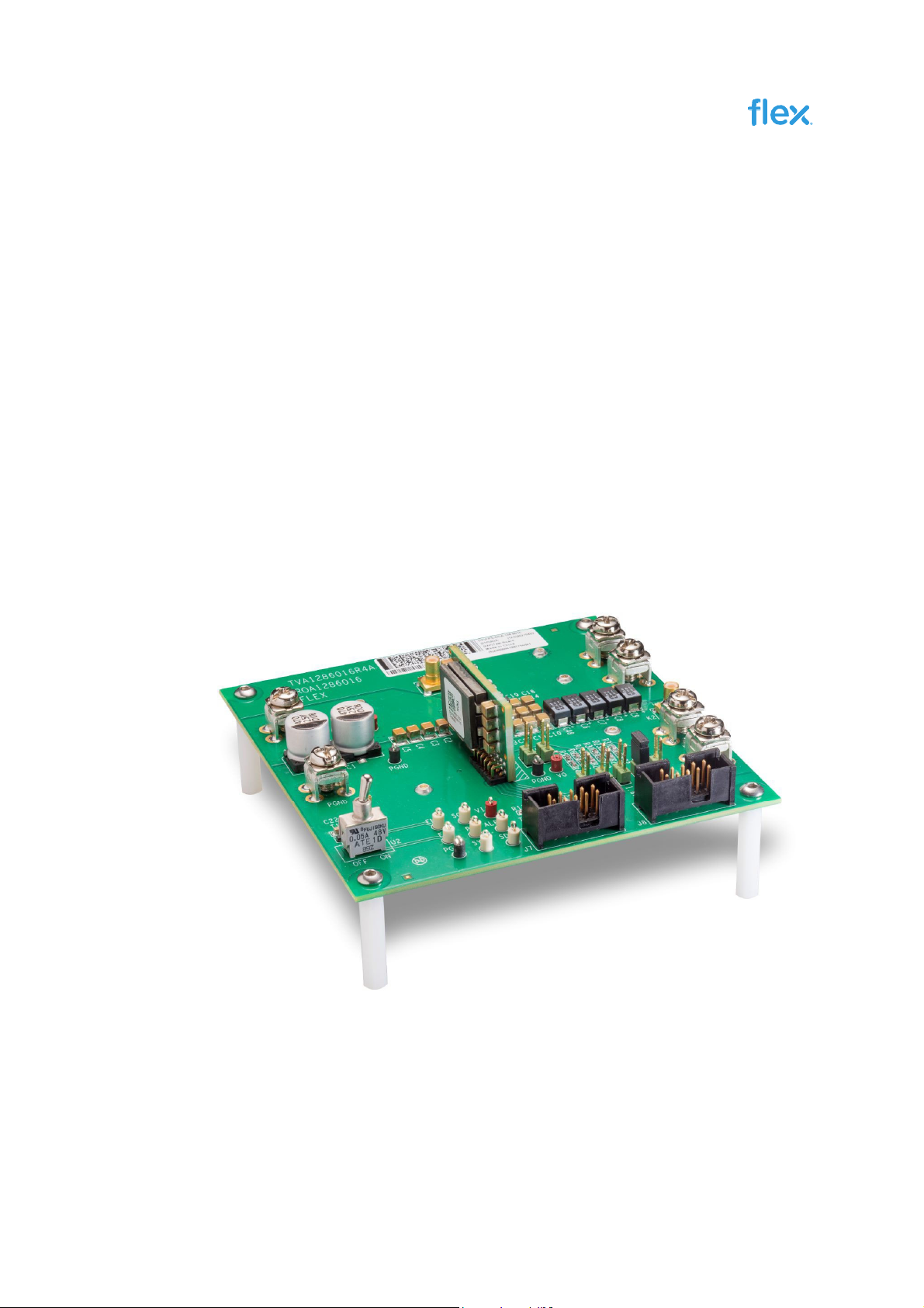
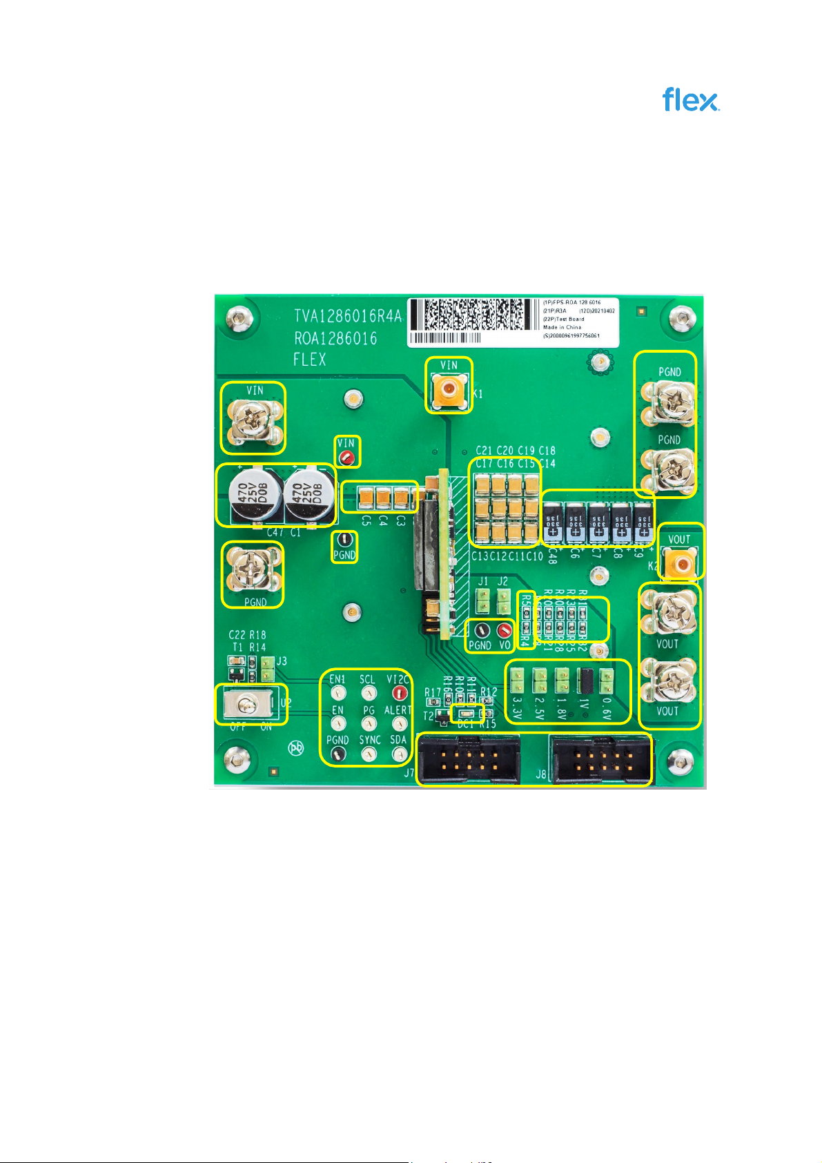
2 Reference Board ROA 128 6016 ...........................................................5
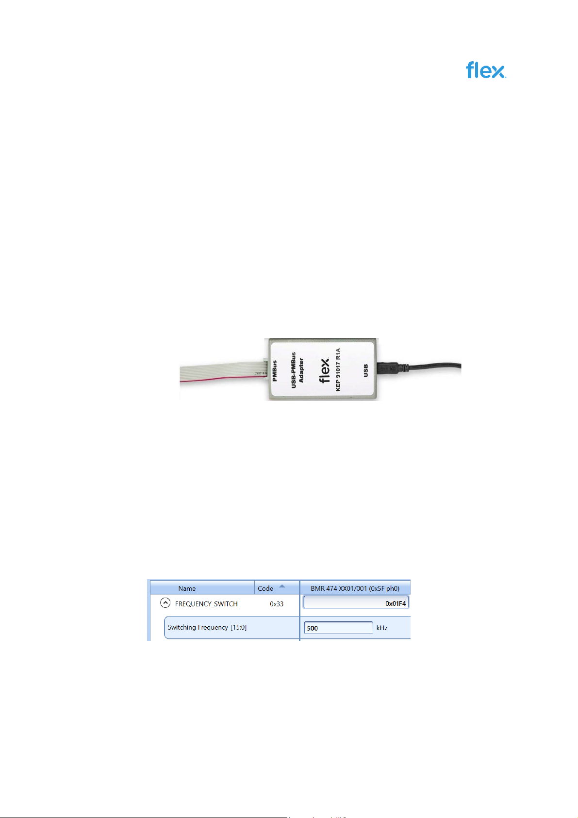
3 USB-PMBus adapter ..............................................................................
7
3.1 Connection of Flex KEP 910 17 USB-PMBus adapter.............................7
4 Power-up and Power-down Instructions .............................................7
4.1 Power-up instruction ................................................................................7
4.2 Power-down instruction............................................................................8
5 Address
and VSET Resistor..................................................................9
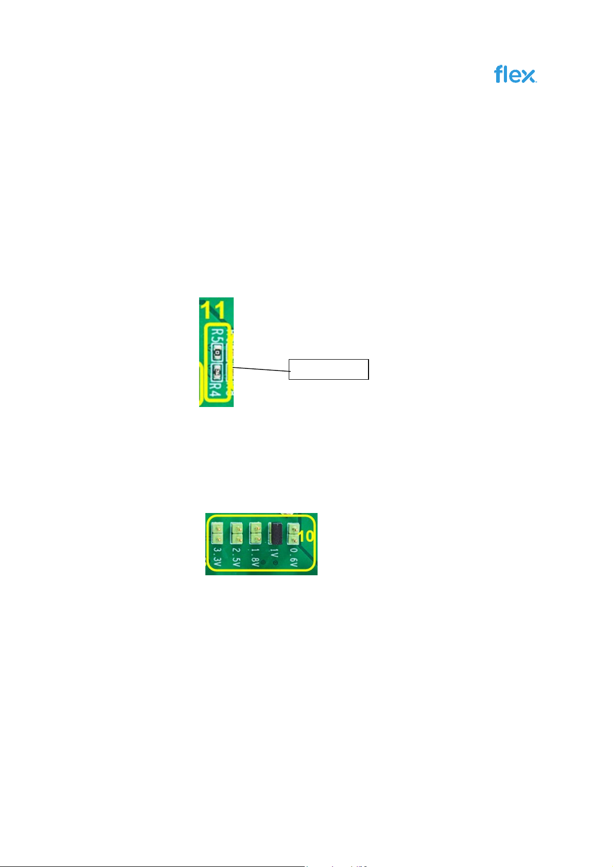
5.1 Adjustment of address resistor.................................................................9
5.2 Adjustment of VSET resistors ..................................................................9
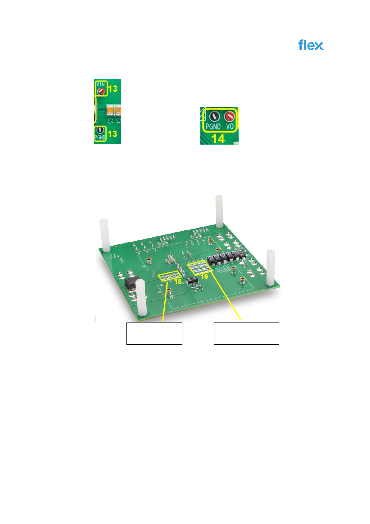
6 Test
points..............................................................................................
9
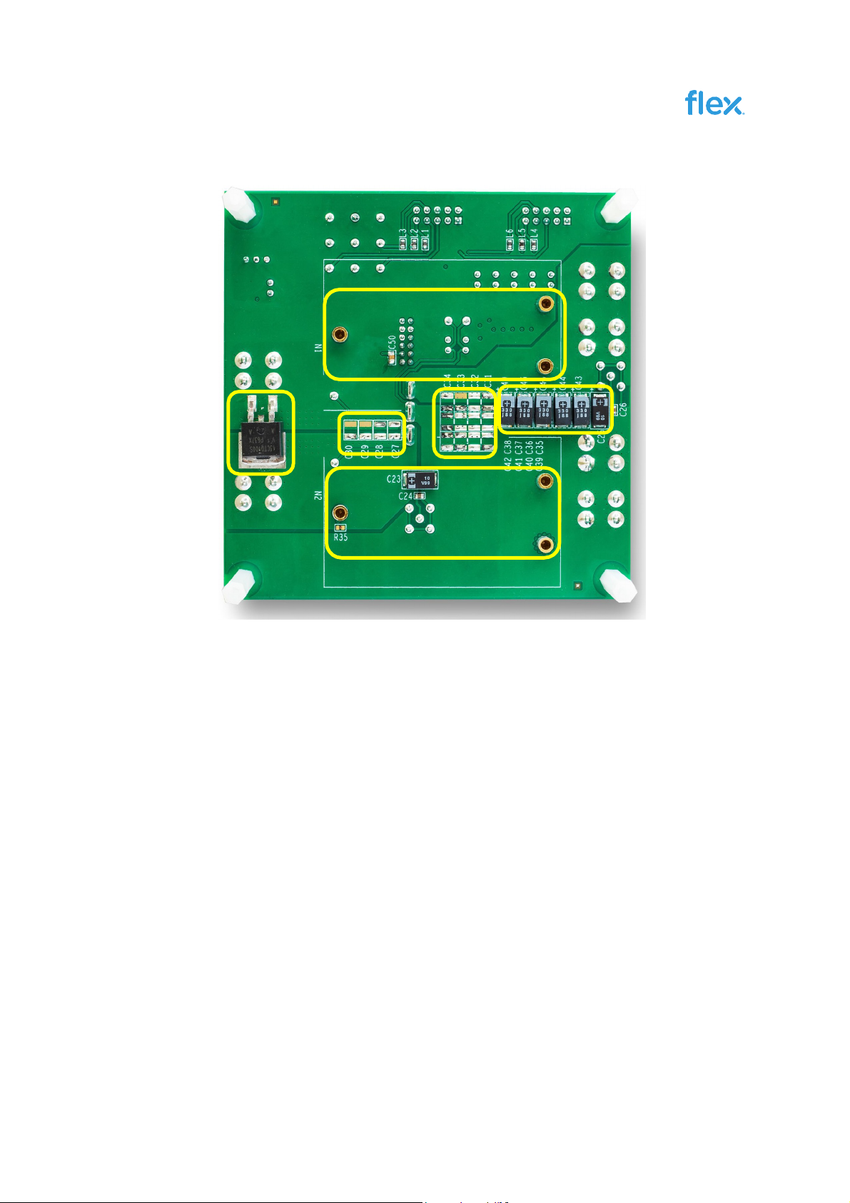
7 Additional
Input/output Capacitance .................................................10
8 Electronic loads ...................................................................................
10
9 Schematic .............................................................................................
11
10 Bill
of Materials.....................................................................................11
11 Layout
description...............................................................................12
11.1 PCB stack-up summary .........................................................................12
11.2 Input capacitance ...................................................................................14
11.3 Output capacitance ................................................................................14
12 Layout
top view ....................................................................................
15